Table of Contents
Advertisement
Quick Links
Advertisement
Table of Contents

Subscribe to Our Youtube Channel
Related Manuals for IEI Technology PCISA-BT


Summary of Contents for IEI Technology PCISA-BT
- Page 1 PCISA-BT CPU Card MODEL: PCISA-BT Half-Size PCISA CPU Card with 22nm Intel® Atom® or Celeron® SoC, Dual Intel® PCIe GbE, VGA, iDP, PCIe Mini, mSATA, USB 3.2 Gen 1, SATA 3Gb/s, COM, HD Audio and RoHS User Manual Page i...
- Page 2 PCISA-BT CPU Card Revision Date Version Changes July 8, 2021 1.10 Updated for R11 version June 30, 2017 1.04 Updated BIOS spec on page 8 July 6, 2016 1.03 Marked LVDS function as optional January 11, 2016 1.02 Changed part number of the optional LPT cable...
- Page 3 PCISA-BT CPU Card Copyright COPYRIGHT NOTICE The information in this document is subject to change without prior notice in order to improve reliability, design and function and does not represent a commitment on the part of the manufacturer. In no event will the manufacturer be liable for direct, indirect, special, incidental, or consequential damages arising out of the use or inability to use the product or documentation, even if advised of the possibility of such damages.
- Page 4 PCISA-BT CPU Card Manual Conventions WARNING Warnings appear where overlooked details may cause damage to the equipment or result in personal injury. Warnings should be taken seriously. CAUTION Cautionary messages should be heeded to help reduce the chance of losing data or damaging the product.
-
Page 5: Table Of Contents
PTIONAL TEMS 3 CONNECTORS ......................15 3.1 P ..............16 ERIPHERAL NTERFACE ONNECTORS 3.1.1 PCISA-BT Layout ..................... 16 3.1.2 Peripheral Interface Connectors ..............17 3.1.3 External Interface Panel Connectors ............... 18 3.2 I ..............18 NTERNAL ERIPHERAL ONNECTORS 3.2.1 ATX Power Supply Enabled Connector ............18 3.2.2 Audio Connector .................... - Page 6 PCISA-BT CPU Card 3.2.10 I C Connector ....................27 3.2.11 Infrared Interface Connector ................. 27 3.2.12 Internal DisplayPort Connector ..............28 3.2.13 Keyboard and Mouse Connector ..............29 3.2.14 LVDS Connector (Optional) ................30 3.2.15 microSD Card Slot ..................31 3.2.16 mSATA Slot .....................
- Page 7 PCISA-BT CPU Card 4.7.1 AT/ATX Power Mode Setting ................59 4.7.2 Clear CMOS Button ..................59 4.7.3 LVDS Panel Type Selection (Optional) ............60 4.7.4 LVDS Backlight Mode Selection (Optional) ............ 61 4.7.5 LVDS Voltage Selection (Optional) ..............62 4.8 I ............
- Page 8 PCISA-BT CPU Card 5.4.2.1 PCI Express Configuration ............... 96 5.5 S ......................... 97 ECURITY 5.6 B ........................98 5.7 S & E ......................100 6 SOFTWARE DRIVERS .................... 101 6.1 A ....................102 VAILABLE RIVERS 6.2 D ....................102 RIVER OWNLOAD A REGULATORY COMPLIANCE ................
- Page 9 List of Figures Figure 1-1: PCISA-BT ........................2 Figure 1-2: Connectors ........................4 Figure 1-3: PCISA-BT Dimensions (mm) ..................5 Figure 1-4: Data Flow Diagram ...................... 6 Figure 3-1: Peripheral Interface Connectors ................16 Figure 3-2: ATX Power Supply Enabled Connector Location ..........19 Figure 3-3: Audio Connector Location ..................
- Page 10 PCISA-BT CPU Card Figure 3-27: SPI Flash Connector Location ................42 Figure 3-28: SPI EC Flash Connector Location ................. 42 Figure 3-29: TPM Connector Location ..................43 Figure 3-30: USB 2.0 Connector (Type A) Pinout Location ............44 Figure 3-31: USB 2.0 Connector Pinout Locations ..............45 Figure 3-32: External Peripheral Interface Connector ..............
- Page 11 PCISA-BT CPU Card List of Tables Table 1-1: Model Variations ......................2 Table 1-2: PCISA-BT Specifications ..................... 9 Table 2-1: Packing List ......................... 12 Table 2-2: Optional Items ......................14 Table 3-1: Peripheral Interface Connectors ................18 Table 3-2: External Peripheral Connectors ................18 Table 3-3: ATX Power Supply Enabled Connector Pinouts .............
- Page 12 PCISA-BT CPU Card Table 3-27: SPI EC Flash Connector Pinouts ................43 Table 3-28: TPM Connector Pinouts ................... 44 Table 3-29: USB 2.0 Connector (Type A) Pinouts ..............45 Table 3-30: USB 2.0 Connector Pinouts ..................45 Table 3-31: LAN Pinouts ......................46 Table 3-32: USB 2.0 Port Pinouts ....................
- Page 13 PCISA-BT CPU Card BIOS Menus BIOS Menu 1: Main ........................68 BIOS Menu 2: Advanced ......................69 BIOS Menu 3: ACPI Configuration ....................70 BIOS Menu 4: F81866 Super IO Configuration ................71 BIOS Menu 5: Serial Port n Configuration Menu ............... 71 BIOS Menu 6: IrDA Configuration Menu ..................
-
Page 15: Introduction
PCISA-BT CPU Card Chapter Introduction Page 1... -
Page 16: Introduction
DDR3L SO-DIMM socket and dual PCI Express (PCIe) Gigabit Ethernet (GbE). The PCISA-BT equips with one USB 3.2 Gen 1 (5Gb/s), six USB 2.0, two SATA 3Gb/s, two RS-232, one RS-422/485, one PCIe Mini slot, one mSATA slot and one microSD slot, providing extreme expansion possibility. -
Page 17: Features
PCISA-BT CPU Card 1.3 Features Some of the PCISA-BT motherboard features are listed below: Half-size PCISA CPU card On-board 22nm Intel® Atom® or Celeron® SoC One 204-pin 1333/1066 MHz unbuffered DDR3L SDRAM SO-DIMM slot supports up to 8 GB ... -
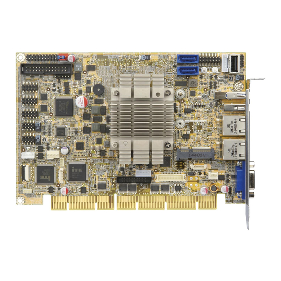
Page 18: Connectors
PCISA-BT CPU Card 1.4 Connectors The connectors on the PCISA-BT are shown in the figure below. Figure 1-2: Connectors Page 4... -
Page 19: Dimensions
PCISA-BT CPU Card 1.5 Dimensions The main dimensions of the PCISA-BT are shown in the diagram below. Figure 1-3: PCISA-BT Dimensions (mm) Page 5... -
Page 20: Data Flow
PCISA-BT CPU Card 1.6 Data Flow Figure 1-4 shows the data flow between the system chipset, the CPU and other components installed on the motherboard. Figure 1-4: Data Flow Diagram Page 6... -
Page 21: Technical Specifications
PCISA-BT CPU Card 1.7 Technical Specifications The PCISA-BT technical specifications are listed below. Specification/Model PCISA-BT Half-size PCISA CPU card Form Factor Intel® Atom® E3845 (1.91GHz, quad-core, 2MB cache, TDP=10W) Intel® Atom® E3827 (1.75GHz, dual-core, 1MB cache, TDP=8W) Intel® Atom® E3826 (1.46GHz, dual-core, 1MB cache, TDP=7W) On-board SoC Intel®... - Page 22 PCISA-BT CPU Card Fintek F81866 Super I/O Controller Software programmable supports 1~255 sec. system reset Watchdog Timer UEFI BIOS B341AIxx BIOS version is for E38xx SoC BIOS B341AMxx BIOS version is for J1900/N2930/N2807 SoC External I/O Interface Connectors Display Output...
-
Page 23: Table 1-2: Pcisa-Bt Specifications
1000 g/250 g Table 1-2: PCISA-BT Specifications NOTE: ISA Limitation of PCISA-BT Due to the limitation of Intel® Bay Trail processors, the PCISA-BT does not support the following features: Bus Master Cycles LPC Memory Mapped Transactions IRQ0, IRQ1, IRQ2, IRQ8, IRQ9, IRQ13, IRQ14... -
Page 24: Packing List
PCISA-BT CPU Card Chapter Packing List Page 10... -
Page 25: Anti-Static Precautions
Only handle the edges of the PCB: Don't touch the surface of the motherboard. Hold the motherboard by the edges when handling. 2.2 Unpacking Precautions When the PCISA-BT is unpacked, please do the following: Follow the anti-static guidelines above. -
Page 26: Packing List
If any of the components listed in the checklist below are missing, do not proceed with the installation. Contact the IEI reseller or vendor the PCISA-BT was purchased from or contact an IEI sales representative directly by sending an email to sales@ieiworld.com. -
Page 27: Optional Items
PCISA-BT CPU Card 2.4 Optional Items The following are optional components which may be separately purchased: Item and Part Number Image RS-422/485 cable, 200 mm (P/N: 32205-003800-300-RS) Dual RS-232 cable, 230 mm, P=2.54 (P/N: 19800-020100-100-RS) PS/2 KB/MS Y-cable with bracket, 220 mm... -
Page 28: Table 2-2: Optional Items
PCISA-BT CPU Card Item and Part Number Image DisplayPort to DVI-D converter board (for IEI iDP connector) (P/N: DP-DVI-R10) DisplayPort to DisplayPort converter board (for IEI iDP connector) (P/N: DP-DP-R10) 20-pin Infineon TPM module, software management tool, firmware v4.4 (P/N: TPM-IN01-R20) -
Page 29: Connectors
PCISA-BT CPU Card Chapter Connectors Page 15... -
Page 30: Peripheral Interface Connectors
PCISA-BT CPU Card 3.1 Peripheral Interface Connectors This chapter details all the peripheral interface connectors. 3.1.1 PCISA-BT Layout The figure below shows all the peripheral interface connectors. Figure 3-1: Peripheral Interface Connectors Page 16... -
Page 31: Peripheral Interface Connectors
PCISA-BT CPU Card 3.1.2 Peripheral Interface Connectors The table below lists all the connectors on the board. Connector Type Label ATX power supply enabled connector 3-pin wafer ATXCTL1 Audio connector 10-pin header J_AUDIO1 Backlight inverter connector (optional) 5-pin wafer INV1... -
Page 32: External Interface Panel Connectors
USB1 VGA connector 15-pin female VGA1 Table 3-2: External Peripheral Connectors 3.2 Internal Peripheral Connectors The section describes all of the connectors on the PCISA-BT. 3.2.1 ATX Power Supply Enabled Connector CN Label: ATXCTL1 3-pin wafer, p=2.54 mm CN Type:... -
Page 33: Audio Connector
PCISA-BT CPU Card The ATX power supply enabled connector enables the PCISA-BT to be connected to an ATX power supply. Refer to Table 3-4 for the configuration of AT/ATX power mode. Figure 3-2: ATX Power Supply Enabled Connector Location Description... -
Page 34: Backlight Inverter Connector (Optional)
PCISA-BT CPU Card This connector allows connection to an external audio kit. Figure 3-3: Audio Connector Location Description Description HDA_SYNC HDA_BIT_CLK HDA_SDOUT HDA_SPKR HDA_SDIN HDA_RST# HDA_VCC HDA_GND HDA_+12V HDA_GND Table 3-5: Audio Connector Pinouts 3.2.3 Backlight Inverter Connector (Optional) CN Label:... -
Page 35: Battery Connector
PCISA-BT CPU Card Figure 3-4: Backlight Inverter Connector Location Description LCD_BKLTCTL GROUND +12V GROUND BACKLIGHT ENABLE Table 3-6: Backlight Inverter Connector Pinouts 3.2.4 Battery Connector CAUTION: Risk of explosion if battery is replaced by an incorrect type. Only certified engineers should replace the on-board battery. -
Page 36: Digital I/O Connector
This is connected to the system battery. The battery provides power to the system clock to retain the time when power is turned off. NOTE: It is recommended to attach the RTC battery onto the system chassis in which the PCISA-BT is installed. Figure 3-5: Battery Connector Location... -
Page 37: Ec Debug Connector
PCISA-BT CPU Card Figure 3-6: Digital I/O Connector Location Description Description Output 3 Output 2 Output 1 Output 0 Input 3 Input 2 Input 1 Input 0 Table 3-8: Digital I/O Connector Pinouts 3.2.6 EC Debug Connector CN Label: 20-pin wafer, p=2 mm... -
Page 38: Fan Connector (Cpu)
PCISA-BT CPU Card Description Description EC_EPP_STB# EC_EPP_AFD# EC_EPP_PD0 EC_EPP_PD1 EC_EPP_INIT# EC_EPP_PD2 EC_EPP_SLIN# EC_EPP_PD3 EC_EPP_PD4 EC_EPP_PD5 EC_EPP_BUSY EC_EPP_PD6 EC_EPP_KSI5 EC_EPP_PD7 EC_EPP_KSI4 Table 3-9: EC Debug Connector Pinouts 3.2.7 Fan Connector (CPU) CN Label: CPU_FAN1 CN Type: 4-pin wafer, p=2.54 mm CN Location:... -
Page 39: Fan Connectors (System)
PCISA-BT CPU Card Description +12V FANIO Table 3-10: CPU Fan Connector Pinouts 3.2.8 Fan Connectors (System) CN Label: SYS_FAN1 CN Type: 3-pin wafer, p=2.54 mm CN Location: See Figure 3-9 CN Pinouts: See Table 3-11 Each fan connector attaches to a system cooling fan. -
Page 40: Front Panel Connector
PCISA-BT CPU Card 3.2.9 Front Panel Connector CN Label: F_PANEL1 14-pin header, p=2.54 mm CN Type: CN Location: See Figure 3-10 CN Pinouts: See Table 3-12 The front panel connector connects to the indicator LEDs and buttons on the computer's front panel. -
Page 41: I 2 C Connector
PCISA-BT CPU Card 3.2.10 I C Connector CN Label: I2C_1 4-pin wafer, p=1.25 mm CN Type: CN Location: See Figure 3-11 CN Pinouts: See Table 3-13 The I C connector is used to connect I C-bus devices to the motherboard. -
Page 42: Internal Displayport Connector
PCISA-BT CPU Card Figure 3-12: Infrared Connector Location Description +V5S IR-RX IR-TX Table 3-14: Infrared Connector Pinouts 3.2.12 Internal DisplayPort Connector CN Label: CN Type: 20-pin box header, p=2 mm CN Location: See Figure 3-13 See Table 3-15 CN Pinouts: The DisplayPort connector supports HDMI, LVDS, VGA, DVI and DisplayPort graphics interfaces with up to 3840x2160 resolutions. -
Page 43: Keyboard And Mouse Connector
PCISA-BT CPU Card Figure 3-13: Internal DisplayPort Connector Location Description Description LANE3N AUXP AUXN LANE0P AUX_CTRL_DET_D LANE1P LANE0N LANE1N LANE2P +3.3V LANE3P LANE2N Table 3-15: Internal DisplayPort Connector Pinouts 3.2.13 Keyboard and Mouse Connector CN Label: KB_MS1 CN Type: 6-pin wafer, p=2 mm... -
Page 44: Lvds Connector (Optional)
PCISA-BT CPU Card Figure 3-14: Keyboard and Mouse Connector Location Description Mouse Data Mouse Clock Keyboard Data Keyboard Clock Table 3-16: Keyboard and Mouse Connector Pinouts 3.2.14 LVDS Connector (Optional) CN Label: LVDS1 CN Type: 30-pin crimp CN Location: See Figure 3-15... -
Page 45: Microsd Card Slot
PCISA-BT CPU Card Figure 3-15: LVDS Connector Location Description Description LVDS_A_TX0-P LVDS_A_TX0-N LVDS_A_TX1-P LVDS_A_TX1-N LVDS_A_TX2-P LVDS_A_TX2-N LVDS_A_TXCLK-P LVDS_A_TXCLK-N LVDS_A_TX3-P LVDS_A_TX3-N LVDS_B_TX0-P LVDS_B_TX0-N LVDS_B_TX1-P LVDS_B_TX1-N LVDS_B_TX2-P LVDS_B_TX2-N LVDS_B_TXCLK-P LVDS_B_TXCLK-N LVDS_B_TX3-P LVDS_B_TX3-N +LCD Vcc +LCD Vcc +LCD Vcc +LCD Vcc Table 3-17: LVDS Connector Pinouts 3.2.15 microSD Card Slot... -
Page 46: Msata Slot
PCISA-BT CPU Card The microSD card slot is for installing a microSD card to the system. Figure 3-16: microSD Card Slot Location 3.2.16 mSATA Slot NOTE: The user can use either the mSATA slot or the SATA2 connector. If an mSATA device is installed to the mSATA slot, the SATA2 connector will be disabled. -
Page 47: Parallel Port Connector
PCISA-BT CPU Card Description Description PCIE_WAKE# +3.3V 1.5V MSATA_CLK# MSATA _CLK PLTRST_N +3.3V PLTRST_N SATA_RX+ +3.3V SATA_RX- 1.5V SMB_CLK SATA_TX- SMB_DATA SATA_TX+ USB_DATA- USB_DATA+ +3.3V +3.3V +3.3V CLINK_CLK CLINK_DATA 1.5V CLINK_RST# MSATA_DET +3.3V Table 3-18: mSATA Slot Pinouts 3.2.17 Parallel Port Connector... -
Page 48: Figure 3-18: Parallel Port Connector Location
PCISA-BT CPU Card CN Location: See Figure 3-18 CN Pinouts: See Table 3-19 The parallel port connector connects to a parallel port connector interface or some other parallel port device such as a printer. Figure 3-18: Parallel Port Connector Location... -
Page 49: Pcie Mini Slot
PCISA-BT CPU Card 3.2.18 PCIe Mini Slot CN Label: M_PCIE1 PCIe Mini slot CN Type: CN Location: See Figure 3-19 CN Pinouts: See Table 3-20 The PCIe Mini slot is for installing a full-size/half-size PCIe Mini expansion card. Figure 3-19: PCIe Mini Slot Location... -
Page 50: Power Button
PCISA-BT CPU Card Description Description PETN0 SMB_DATA PETP0 USB_D- USB_D+ LED_WWAN# LED_WLAN# LED_WPAN# 1.5V 3.3V Table 3-20: PCIe Mini Slot Pinouts 3.2.19 Power Button CN Label: PWR_SW1 Push button CN Type: CN Location: See Figure 3-20 The on-board power button controls system power. -
Page 51: Reset Button
Push button CN Type: CN Location: See Figure 3-21 Push the on-board reset button to reset the PCISA-BT. Figure 3-21: Reset Button Location 3.2.21 SATA 3Gb/s Drive Connector NOTE: The user can use either the mSATA slot or the SATA2 connector. If an mSATA device is installed to the mSATA slot, the SATA2 connector will be disabled. -
Page 52: Serial Port Connector, Rs-232
PCISA-BT CPU Card The SATA drive connectors can be connected to SATA drives and supports up to 3Gb/s data transfer rate. Figure 3-22: SATA 3Gb/s Drive Connector Locations Description Description Table 3-21: SATA 3Gb/s Drive Connector Pinouts 3.2.22 Serial Port Connector, RS-232... -
Page 53: Serial Port Connector, Rs-422/485
PCISA-BT CPU Card Figure 3-23: RS-232 Serial Port Connector Locations Description Description Table 3-22: RS-232 Serial Port Connector Pinouts 3.2.23 Serial Port Connector, RS-422/485 CN Label: COM3 CN Type: 4-pin wafer, p=2 mm CN Location: See Figure 3-24 CN Pinouts: See Table 3-23 This connector provides RS-422 or RS-485 communications. -
Page 54: Smbus Connector
PCISA-BT CPU Card Description Description RXD422- TXD422+/TXD485+ RXD422+ TXD422-/TXD485- Table 3-23: RS-422/485 Connector Pinouts Use the optional RS-422/485 cable to connect to a serial device. The pinouts of the DB-9 connector are listed below. RS-422 Pinouts RS-485 Pinouts Table 3-24: DB-9 RS-422/485 Pinouts 3.2.24 SMBus Connector... -
Page 55: So-Dimm Slot
PCISA-BT CPU Card Description SMB_DATA SMB_CLK Table 3-25: SMBus Connector Pinouts 3.2.25 SO-DIMM Slot CN Label: DIMM1 DDR3L SO-DIMM slot CN Type: CN Location: See Figure 3-26 The SO-DIMM slot is for installing a DDR3L SO-DIMM. Figure 3-26: SO-DIMM Slot Location 3.2.26 SPI Flash Connector... -
Page 56: Spi Flash Connector, Ec
PCISA-BT CPU Card Figure 3-27: SPI Flash Connector Location Description Description SPI_CS# +1.8V SPI_SO SPI_CLK SPI_SI Table 3-26: SPI Flash Connector Pinouts 3.2.27 SPI Flash Connector, EC CN Label: JSPI2 CN Type: 6-pin wafer, p=2.54 mm CN Location: See Figure 3-28... -
Page 57: Tpm Connector
PCISA-BT CPU Card Description Description +3.3V SPI_CS# SPI_SO SPI_CLK SPI_SI Table 3-27: SPI EC Flash Connector Pinouts 3.2.28 TPM Connector CN Label: TPM1 CN Type: 20-pin header, p=2.54 mm CN Location: See Figure 3-29 CN Pinouts: See Table 3-28 The TPM connector connects to a TPM module. -
Page 58: Usb 2.0 Connector (Type A)
PCISA-BT CPU Card Description Description SB3V SERIRQ GLKRUN# LPCPD# LDRQ# Table 3-28: TPM Connector Pinouts 3.2.29 USB 2.0 Connector (Type A) CN Label: USB5 CN Type: USB Type A CN Location: See Figure 3-30 CN Pinouts: See Table 3-29 The USB Type A connector connects to a USB 2.0/1.1 device. -
Page 59: Usb 2.0 Connectors
PCISA-BT CPU Card Description DATA- DATA+ GROUND Table 3-29: USB 2.0 Connector (Type A) Pinouts 3.2.30 USB 2.0 Connectors CN Label: USB3, USB4 8-pin header, p=2.54 mm CN Type: CN Location: See Figure 3-31 CN Pinouts: See Table 3-30 The USB 2.0 connectors connect to USB 2.0 devices. Each pin header provides two USB 2.0 ports. -
Page 60: External Peripheral Interface Connector Panel
PCISA-BT CPU Card 3.3 External Peripheral Interface Connector Panel The figure below shows the external peripheral interface connector (EPIC) panel. The EPIC panel consists of the following: Figure 3-32: External Peripheral Interface Connector 3.3.1 Ethernet Connectors CN Label: LAN1, LAN2... -
Page 61: Usb 2.0 Connector
CN Label: USB1 CN Type: USB Type-A CN Location: See Figure 3-32 CN Pinouts: See Table 3-33 There is one external USB 3.2 Gen 1 (5Gb/s) connector on the PCISA-BT. Description Description USB3.0RX+ USB_DATA- AGND USB_DATA+ USB3.0 TX+ USB3.0 TX- USB3.0RX-... -
Page 62: Vga Connector
PCISA-BT CPU Card 3.3.4 VGA Connector CN Label: VGA1 15-pin VGA CN Type: CN Location: See Figure 3-32 CN Pinouts: See Table 3-34 The 15-pin VGA connector connects to a monitor that accepts a standard VGA input. Description Description GREEN... -
Page 63: Installation
PCISA-BT CPU Card Chapter Installation Page 49... -
Page 64: Anti-Static Precautions
Electrostatic discharge (ESD) can cause serious damage to electronic components, including the PCISA-BT. Dry climates are especially susceptible to ESD. It is therefore critical that whenever the PCISA-BT or any other electrical component is handled, the following anti-static precautions are strictly adhered to. - Page 65 Turn all power to the PCISA-BT off: When working with the PCISA-BT, make sure that it is disconnected from all power supplies and that no electricity is being fed into the system. Before and during the installation of the PCISA-BT, DO NOT: ...
-
Page 66: So-Dimm Installation
To install a SO-DIMM, please follow the steps below and refer to Figure 4-1. Figure 4-1: SO-DIMM Installation Step 1: Locate the SO-DIMM socket on the solder side of the PCISA-BT. Place the board on an anti-static mat. Step 2: Align the SO-DIMM with the socket. -
Page 67: Figure 4-2: Removing The Retention Screw
PCISA-BT CPU Card Figure 4-2: Removing the Retention Screw Step 3: Insert into the socket at an angle. Line up the notch on the card with the notch on the slot. Slide the PCIe Mini card into the socket at an angle of about 20º... -
Page 68: Half-Size Pcie Mini Card Installation
PCISA-BT CPU Card Step 4: Secure the full-size PCIe Mini card. Secure the full-size PCIe Mini card with the retention screw previously removed (Figure 4-4). Step 0: Figure 4-4: Securing the Full-size PCIe Mini Card 4.5 Half-size PCIe Mini Card Installation The PCIe Mini card slot allows installation of either a full-size or half-size PCIe Mini card. -
Page 69: Figure 4-5: Removing The Standoff
PCISA-BT CPU Card Figure 4-5: Removing the Standoff Step 4: Install the standoff to the screw hole for the half-size PCIe Mini card. Install the previously removed standoff to the screw hole for the half-size PCIe Mini card (Figure 4-6). -
Page 70: Figure 4-7: Inserting The Half-Size Pcie Mini Card Into The Slot At An Angle
PCISA-BT CPU Card Step 5: Insert into the socket at an angle. Line up the notch on the card with the notch on the slot. Slide the PCIe Mini card into the slot at an angle of about 20º (Figure 4-7). -
Page 71: Msata Module Installation
PCISA-BT CPU Card 4.6 mSATA Module Installation NOTE: The user can use either the mSATA slot or the SATA2 connector. If an mSATA device is installed to the mSATA slot (M_SATA1), the SATA2 connector will be disabled. To install an mSATA module, please follow the steps below. -
Page 72: Figure 4-10: Inserting The Msata Module Into The Socket At An Angle
PCISA-BT CPU Card Figure 4-10: Inserting the mSATA Module into the Socket at an Angle Step 4: Secure the mSATA module. Secure the mSATA module with the retention screws previously removed (Figure 4-11). Step 0: Figure 4-11: Securing the mSATA Module... -
Page 73: System Configuration
PCISA-BT CPU Card 4.7 System Configuration The system configuration should be performed before installation. 4.7.1 AT/ATX Power Mode Setting The AT and ATX power mode selection is made through the AT/ATX power mode switch which is shown in Figure 4-12. -
Page 74: Lvds Panel Type Selection (Optional)
PCISA-BT CPU Card 4.7.3 LVDS Panel Type Selection (Optional) Jumper Label: DIP switch Jumper Type: Jumper Settings: See Table 4-2 Jumper Location: See Figure 4-14 Use the DIP switch to select the resolution of the LCD panel connected to the LVDS1 connector. -
Page 75: Lvds Backlight Mode Selection (Optional)
PCISA-BT CPU Card Figure 4-14: LVDS Panel Type Selection Switch Location 4.7.4 LVDS Backlight Mode Selection (Optional) Jumper Label: Jumper Type: 3-pin header See Table 4-3 Jumper Settings: Jumper Location: See Figure 4-15 The LVDS backlight mode selection jumper allows setting the backlight mode of the monitor connected to the LVDS connector. -
Page 76: Lvds Voltage Selection (Optional)
4.7.5 LVDS Voltage Selection (Optional) WARNING: Permanent damage to the screen and PCISA-BT may occur if the wrong voltage is selected with this jumper. Please refer to the user guide that came with the monitor to select the correct voltage. -
Page 77: Internal Peripheral Device Connections
This section outlines the installation of peripheral devices to the onboard connectors. 4.8.1 SATA Drive Connection The PCISA-BT is shipped with two SATA drive cables. To connect the SATA drives to the connectors, please follow the steps below. Step 1: Locate the connectors. -
Page 78: Figure 4-18: Sata Power Drive Connection
PCISA-BT CPU Card Figure 4-18: SATA Power Drive Connection The SATA power cable can be bought from IEI. See Optional Items in Section 2.4. Page 64... -
Page 79: Bios
PCISA-BT CPU Card Chapter BIOS Page 65... -
Page 80: Introduction
PCISA-BT CPU Card 5.1 Introduction The BIOS is programmed onto the BIOS chip. The BIOS setup program allows changes to certain system settings. This chapter outlines the options that can be changed. NOTE: Some of the BIOS options may vary throughout the life cycle of the product and are subject to change without prior notice. -
Page 81: Getting Help
PCISA-BT CPU Card Function Page Up Move to the previous page Page Dn Move to the next page Main Menu – Quit and not save changes into CMOS Status Page Setup Menu and Option Page Setup Menu -- Exit current page and return to Main Menu... -
Page 82: Main
PCISA-BT CPU Card 5.2 Main The Main BIOS menu (BIOS Menu 1) appears when the BIOS Setup program is entered. The Main menu gives an overview of the basic system information. Aptio Setup Utility – Copyright (C) 2013 American Megatrends, Inc. -
Page 83: Advanced
PCISA-BT CPU Card 5.3 Advanced Use the Advanced menu (BIOS Menu 2) to configure the CPU and peripheral devices through the following sub-menus: WARNING! Setting the wrong values in the sections below may cause the system to malfunction. Make sure that the settings made are compatible with the hardware. -
Page 84: Acpi Settings
PCISA-BT CPU Card 5.3.1 ACPI Settings The ACPI Settings menu (BIOS Menu 3) configures the Advanced Configuration and Power Interface (ACPI) options. Aptio Setup Utility – Copyright (C) 2013 American Megatrends, Inc. Advanced ACPI Settings Select the highest ACPI sleep state the system... -
Page 85: F81866 Super Io Configuration
PCISA-BT CPU Card 5.3.2 F81866 Super IO Configuration Use the F81866 Super IO Configuration menu (BIOS Menu 4) to set or change the configurations for the serial ports and parallel port. Aptio Setup Utility – Copyright (C) 2013 American Megatrends, Inc. - Page 86 PCISA-BT CPU Card 5.3.2.1.1 Serial Port 1 Configuration Serial Port [Enabled] Use the Serial Port option to enable or disable the serial port. Disabled Disable the serial port Enabled Enable the serial port EFAULT Change Settings [Auto] Use the Change Settings option to change the serial port IO port address and interrupt address.
- Page 87 PCISA-BT CPU Card Change Settings [Auto] Use the Change Settings option to change the serial port IO port address and interrupt address. Auto The serial port IO port address and interrupt address EFAULT are automatically detected. Serial Port I/O port address is 2F8h and the interrupt IO=2F8h;...
- Page 88 PCISA-BT CPU Card IO=3E8h; Serial Port I/O port address is 3E8h and the interrupt IRQ=10 address is IRQ10 Serial Port I/O port address is 3F8h and the interrupt IO=3F8h; address is IRQ10, 11 IRQ=10, 11 IO=2F8h; Serial Port I/O port address is 2F8h and the interrupt...
- Page 89 PCISA-BT CPU Card IO=2D0h; Serial Port I/O port address is 2D0h and the interrupt IRQ=10, 11 address is IRQ10, 11 Serial Port I/O port address is 2D8h and the interrupt IO=2D8h; address is IRQ10, 11 IRQ=10, 11 ...
- Page 90 PCISA-BT CPU Card IO=2D8h; Serial Port I/O port address is 2D8h and the interrupt IRQ=10, 11 address is IRQ10, 11 Serial Port I/O port address is 2E0h and the interrupt IO=2E0h; address is IRQ10, 11 IRQ=10, 11 ...
-
Page 91: Irda Configuration
PCISA-BT CPU Card IO=2E0h; Serial Port I/O port address is 2E0h and the interrupt IRQ=10, 11 address is IRQ10, 11 Serial Port I/O port address is 2E8h and the interrupt IO=2E8h; address is IRQ10, 11 IRQ=10, 11 5.3.2.2 IrDA Configuration Use the IrDA Configuration menu (BIOS Menu 6) to configure the infrared port. - Page 92 PCISA-BT CPU Card Auto The serial port IO port address and interrupt address EFAULT are automatically detected. Serial Port I/O port address is 2E0h and the interrupt IO=2E0h; address is IRQ11 IRQ=11 IO=3F8h; Serial Port I/O port address is 3F8h and the interrupt...
-
Page 93: Parallel Port Configuration
PCISA-BT CPU Card 5.3.2.3 Parallel Port Configuration Use the Parallel Port Configuration menu (BIOS Menu 7) to configure the serial port n. Aptio Setup Utility – Copyright (C) 2010 American Megatrends, Inc. Advanced Parallel Port Configuration Enable or Disable Parallel Port (LPT/LPTE) - Page 94 PCISA-BT CPU Card IO=378h; Parallel Port I/O port address is 378h and the IRQ=5, 6, interrupt address is IRQ5, 6, 7, 9, 10, 11 12 7, 9, 10, 11, IO=278h; Parallel Port I/O port address is 278h and the...
-
Page 95: Iwdd H/W Monitor
PCISA-BT CPU Card 5.3.3 iWDD H/W Monitor The iWDD H/W Monitor menu (BIOS Menu 8) contains the fan configuration submenu, and displays operating temperature, fan speeds and system voltages.. Aptio Setup Utility – Copyright (C) 2013 American Megatrends, Inc. Advanced... -
Page 96: Smart Fan Mode Configuration
PCISA-BT CPU Card +5VSB +3.3V +3.3VSB 5.3.3.1 Smart Fan Mode Configuration Use the Smart Fan Mode Configuration submenu (BIOS Menu 9) to configure fan speed settings. Aptio Setup Utility – Copyright (C) 2013 American Megatrends, Inc. Advanced Smart Fan Mode Configuration... -
Page 97: Rtc Wake Settings
PCISA-BT CPU Card Auto mode fan start PWM Use the + or – key to change the Auto mode fan start PWM value. Enter a decimal number between 1 and 100. Auto mode fan slope PWM Use the + or – key to change the Auto mode fan slope PWM value. Enter a decimal number between 1 and 8. -
Page 98: Serial Port Console Redirection
PCISA-BT CPU Card Enabled If selected, the Wake up every day option appears allowing you to enable to disable the system to wake every day at the specified time. Besides, the following options appear with values that can be... - Page 99 PCISA-BT CPU Card Console Redirection [Disabled] Use Console Redirection option to enable or disable the console redirection function. Disabled the console redirection function Disabled EFAULT Enabled the console redirection function Enabled The following options are available in the Console Redirection Settings submenu when the Console Redirection option is enabled.
- Page 100 PCISA-BT CPU Card Parity [None] Use the Parity option to specify the parity bit that can be sent with the data bits for detecting the transmission errors. None No parity bit is sent with the data bits. EFAULT ...
-
Page 101: Iei Feature
PCISA-BT CPU Card 5.3.6 iEi Feature Use the iEi Feature menu (BIOS Menu 12) to configure One Key Recovery function. Aptio Setup Utility – Copyright (C) 2013 American Megatrends, Inc. Advanced iEi Feature Auto Recovery Function Reboot and recover Auto Recovery Function... -
Page 102: Cpu Configuration
PCISA-BT CPU Card 5.3.7 CPU Configuration Use the CPU Configuration menu (BIOS Menu 13) to view detailed CPU specifications or enable the Intel Virtualization Technology. Aptio Setup Utility – Copyright (C) 2013 American Megatrends, Inc. Advanced CPU Information When enabled, a VMM can utilize the additional Intel(R) Atom(R) CPU E3845 @ 1.91GHz... -
Page 103: Ide Configuration
PCISA-BT CPU Card Disabled Disables Enhanced Intel® SpeedStep Technology Enables Enhanced Intel® SpeedStep Technology Enabled EFAULT 5.3.8 IDE Configuration Use the IDE Configuration menu (BIOS Menu 14) to change and/or set the configuration of the SATA devices installed in the system. -
Page 104: Trusted Computing
PCISA-BT CPU Card 5.3.9 Trusted Computing Use the Trusted Computing menu (BIOS Menu 15) to configure settings related to the Trusted Computing Group (TCG) Trusted Platform Module (TPM). Aptio Setup Utility – Copyright (C) 2013 American Megatrends, Inc. Advanced Configuration... -
Page 105: Usb Configuration
PCISA-BT CPU Card 5.3.10 USB Configuration Use the USB Configuration menu (BIOS Menu 16) to read USB configuration information and configure the USB settings. Aptio Setup Utility – Copyright (C) 2013 American Megatrends, Inc. Advanced USB Configuration Enables Legacy USB support. -
Page 106: Chipset
PCISA-BT CPU Card 5.4 Chipset Use the Chipset menu (BIOS Menu 17) to access the PCH IO and System Agent (SA) configuration menus. WARNING! Setting the wrong values for the Chipset BIOS selections in the Chipset BIOS menu may cause the system to malfunction. -
Page 107: North Bridge
PCISA-BT CPU Card 5.4.1 North Bridge Use the North Bridge menu (BIOS Menu 18) to configure the north bridge parameters. Aptio Setup Utility – Copyright (C) 2013 American Megatrends, Inc. Chipset > Intel IGD Configuration Configure Intel IGD Settings. Memory Information... - Page 108 PCISA-BT CPU Card Primary Display [Auto] Use the Primary Display option to select the display device used by the system when it boots. Configuration options are listed below. Auto EFAULT DVMT Pre-Allocated [256M] Use the DVMT Pre-Allocated option to specify the amount of system memory that can be used by the internal graphics device.
-
Page 109: South Bridge
PCISA-BT CPU Card LVDS (Optional) 5.4.2 South Bridge Use the South Bridge menu (BIOS Menu 20) to configure the south bridge parameters. Aptio Setup Utility – Copyright (C) 2013 American Megatrends, Inc. Chipset Auto Power Button Status... -
Page 110: Pci Express Configuration
PCISA-BT CPU Card Disabled The High Definition Audio controller is disabled. The High Definition Audio controller is enabled. Enabled EFAULT XHCI Mode [Smart Auto] Use the XHCI Mode BIOS option to configure the USB xHCI (USB 3.2 Gen 1) controller. -
Page 111: Security
PCISA-BT CPU Card Speed [Auto] Use the Speed option to configure the speed of PCIe Mini slot. Auto EFAULT Gen 2 Gen 1 5.5 Security Use the Security menu (BIOS Menu 22) to set system and user passwords. -
Page 112: Boot
PCISA-BT CPU Card 5.6 Boot Use the Boot menu (BIOS Menu 23) to configure system boot options. Aptio Setup Utility – Copyright (C) 2013 American Megatrends, Inc. Main Advanced Chipset Security Boot Save & Exit Boot Configuration Select the keyboard... - Page 113 PCISA-BT CPU Card Quiet Boot [Enabled] Use the Quiet Boot BIOS option to select the screen display when the system boots. Normal POST messages displayed Disabled OEM Logo displayed instead of POST messages Enabled EFAULT UEFI Boot [Disabled] Use the UEFI Boot option to enable or disable to boot from the UEFI devices.
-
Page 114: Save & Exit
PCISA-BT CPU Card 5.7 Save & Exit Use the Safe & Exit menu (BIOS Menu 24) to load default BIOS values, optimal failsafe values and to save configuration changes. Aptio Setup Utility – Copyright (C) 2013 American Megatrends, Inc. Main... -
Page 115: Software Drivers
PCISA-BT CPU Card Chapter Software Drivers Page 101... -
Page 116: Available Drivers
PCISA-BT CPU Card 6.1 Available Drivers All the drivers for the PCISA-BT are available on IEI Resource Download Center (https://download.ieiworld.com). Type PCISA-BT and press Enter to find all the relevant software, utilities, and documentation. Figure 6-1: IEI Resource Download Center 6.2 Driver Download... - Page 117 PCISA-BT CPU Card Step 3: Click the driver file name on the page and you will be prompted with the following window. You can download the entire ISO file ( ), or double click an individual item to find its driver file and click the file name to download (...
-
Page 118: A Regulatory Compliance
PCISA-BT CPU Card Appendix Regulatory Compliance Page 104... - Page 119 PCISA-BT CPU Card DECLARATION OF CONFORMITY This equipment has been tested and found to comply with specifications for CE marking. If the user modifies and/or installs other devices in the equipment, the CE conformity declaration may no longer apply. FCC WARNING This equipment complies with Part 15 of the FCC Rules.
-
Page 120: B Product Disposal
PCISA-BT CPU Card Appendix Product Disposal Page 106... - Page 121 PCISA-BT CPU Card CAUTION: Risk of explosion if battery is replaced by an incorrect type. Only certified engineers should replace the on-board battery. Dispose of used batteries according to instructions and local regulations. Outside the European Union–If you wish to dispose of used electrical and electronic products outside the European Union, please contact your local authority so as to comply with the correct disposal method.
-
Page 122: Cbios Options
PCISA-BT CPU Card Appendix BIOS Options Page 108... - Page 123 PCISA-BT CPU Card Below is a list of BIOS configuration options in the BIOS chapter. System Date [xx/xx/xx] ......................68 System Time [xx:xx:xx] ....................... 68 ACPI Sleep State [S3 (Suspend to RAM)] ................70 Serial Port [Enabled] ......................72 Change Settings [Auto] ....................... 72 Serial Port [Enabled] ......................
- Page 124 PCISA-BT CPU Card Stop Bits [1] .......................... 86 Auto Recovery Function [Disabled] ................... 87 Intel Virtualization Technology [Disabled] ................ 88 EIST [Enabled] ........................88 Serial-ATA (SATA) [Enabled] ....................89 SATA Mode [IDE Mode] ....................... 89 Security Device Support [Disabled] ................... 90 USB Devices .........................
-
Page 125: D Digital I/O Interface
PCISA-BT CPU Card Appendix Digital I/O Interface Page 111... -
Page 126: Introduction
PCISA-BT CPU Card D.1 Introduction The DIO connector on the PCISA-BT is interfaced to GPIO ports on the Super I/O chipset. The digital inputs and digital outputs are generally control signals that control the on/off circuit of external devices or TTL devices. Data can be read or written to the selected address to enable the DIO functions. -
Page 127: Assembly Language Sample 1
PCISA-BT CPU Card D.2 Assembly Language Sample 1 AX, 6F08H ;setting the digital port as input AL low byte = value AH – 6FH Sub-function: AL – 9 :Set the digital port as OUTPUT :Digital I/O input value D.3 Assembly Language Sample 2 AX, 6F09H ;setting the digital port as output... -
Page 128: E Watchdog Timer
PCISA-BT CPU Card Appendix Watchdog Timer Page 114... - Page 129 PCISA-BT CPU Card NOTE: The following discussion applies to DOS environment. Contact IEI support or visit the IEI website for specific drivers for other operating systems. The Watchdog Timer is provided to ensure that standalone systems can always recover from catastrophic conditions that cause the CPU to crash. This condition may have occurred by external EMIs or a software bug.
- Page 130 PCISA-BT CPU Card NOTE: When exiting a program it is necessary to disable the Watchdog Timer, otherwise the system resets. EXAMPLE PROGRAM: ; INITIAL TIMER PERIOD COUNTER W_LOOP: AX, 6F02H ;setting the time-out value BL, 30 ;time-out value is 48 seconds ;...
-
Page 131: F Error Beep Code
PCISA-BT CPU Card Appendix Error Beep Code Page 117... -
Page 132: Pei Beep Codes
PCISA-BT CPU Card F.1 PEI Beep Codes Number of Beeps Description Memory not Installed Memory was installed twice (InstallPeiMemory routine in PEI Core called twice) Recovery started DXEIPL was not found DXE Core Firmware Volume was not found Recovery failed... -
Page 133: G Hazardous Materials Disclosure
PCISA-BT CPU Card Appendix Hazardous Materials Disclosure Page 119... -
Page 134: Rohs Ii Directive (2015/863/Eu)
PCISA-BT CPU Card G.1 RoHS II Directive (2015/863/EU) The details provided in this appendix are to ensure that the product is compliant with the RoHS II Directive (2015/863/EU). The table below acknowledges the presences of small quantities of certain substances in the product, and is applicable to RoHS II Directive (2015/863/EU). -
Page 135: China Rohs
PCISA-BT CPU Card G.2 China RoHS 此附件旨在确保本产品符合中国 RoHS 标准。以下表格标示此产品中某有毒物质的含量符 合中国 RoHS 标准规定的限量要求。 本产品上会附有”环境友好使用期限”的标签,此期限是估算这些物质”不会有泄漏或突变”的 年限。本产品可能包含有较短的环境友好使用期限的可替换元件,像是电池或灯管,这些 元件将会单独标示出来。 部件名称 有毒有害物质或元素 壳体 显示 印刷电路板 金属螺帽 电缆组装 风扇组装 电力供应组装 电池 O: 表示该有毒有害物质在该部件所有物质材料中的含量均在 SJ/T11364-2014 與 GB/T26572-2011 标准规定的限量要求以下。 X: 表示该有毒有害物质至少在该部件的某一均质材料中的含量超出 SJ/T11364-2014 與 GB/T26572-2011 标准规定的限量要求。 Page 121...
Need help?
Do you have a question about the PCISA-BT and is the answer not in the manual?
Questions and answers