Table of Contents
Advertisement
Quick Links
USB3-FRM13_K
Windows, Windows2000, Windows NT and Windows XP are trademarks of Microsoft. We acknowledge that the
trademarks or service names of all other organizations mentioned in this document as their own property.
Information furnished by DAQ system is believed to be accurate and reliable. However, no responsibility is assumed by DAQ
system for its use, nor for any infringements of patents or other rights of third parties which may result from its use. No license is
granted by implication or otherwise under any patent or copyrights of DAQ system.
The information in this document is subject to change without notice and no part of this document may be copied or
reproduced without the prior written consent.
User's Manual
Copyrights 2005 DAQ system, All rights reserved.
1
-
-
USB3-FRM13_K Users Manual (Rev 1.1)
http://www.daqsystem.com
Advertisement
Table of Contents

Related Manuals for DAQ system USB3-FRM13-K


Summary of Contents for DAQ system USB3-FRM13-K
- Page 1 Information furnished by DAQ system is believed to be accurate and reliable. However, no responsibility is assumed by DAQ system for its use, nor for any infringements of patents or other rights of third parties which may result from its use. No license is granted by implication or otherwise under any patent or copyrights of DAQ system.
-
Page 2: Table Of Contents
USB3-FRM13_K Users Manual (Rev 1.1) -- Contents – 1. Introduction 2. USB3-FRM13_K Function 2.1 Block Diagram 2.2 Camera Link 2.3 Camera Link and USB3-FRM13_K 2.4 Camera Link Cable 2.5 PoCL 2.6 Area Trigger Mode 3. USB3-FRM13_K Board Description 3.1 USB3-FRM13_K Layout 3.2 Functional Blocks 3.3 Connector Pin-out 3.3.1 CN1 Connecter... -
Page 3: Introduction
DAQ system provides a sample program to use the board briefly so you can test the API provided insource form, so the user can be used to modify. Please refer to Chapter 5 for a detailed description of this sample program. - Page 4 USB3-FRM13_K Users Manual (Rev 1.1) [USB3-FRM13_K Features] Supports Camera Link Base Configuration Camera Supports Camera Link Medium/Full Configuration Camera Support Area Scan Camera, Line Scan Camera USB 3.0 Specification (10x faster than USB2.0) 256MByte Image Buffer ...
-
Page 5: Usb3-Frm13_K Function
USB3-FRM13_K Users Manual (Rev 1.1) 2. USB3-FRM13_K Function 2.1 Block Diagram As shown in the following figure, main control of the board is performed in FPGA Core Logic. The primary functions are writing to the DDR#1, DDR#2 memory after receiving the frame data from two Mini MDR-26, and sent to PC by the request. -
Page 6: Camera Link
USB3-FRM13_K Users Manual (Rev 1.1) 2.2 Camera Link Camera Link is a communication interface for use in a vision application development. In the past, the camera manufacturer and Frame Grabber manufacturers use their own standard connectors and cables. This has caused a lot of confusion and increased costs to users. In order to eliminate this confusion and increase the data rate and data transmission trouble, the specifications of Camera Link interface have been made to the regulations of cable or connector assembly specifications, transfer speed, transfer method at the meeting of camera makers and Frame grabber... - Page 7 USB3-FRM13_K Users Manual (Rev 1.1) the Receiver part of Frame Grabber. [Figure 2-2. Base Camera Link Block Diagram] http://www.daqsystem.com...
- Page 8 USB3-FRM13_K Users Manual (Rev 1.1) [Figure 2-3. Full Camera Link Block Diagram] http://www.daqsystem.com...
- Page 9 USB3-FRM13_K Users Manual (Rev 1.1) 2.3 Camera Link Cable & Connecter The connection between the camera link cameras and USB3-FRM13_K board uses the 26 Pin Mini MDR (Mini D Ribbon) cable. Camera Link cable consists of twin-axial shielded cable and 2 Mini MDR 26-male plug.
-
Page 10: Camera Link And Usb3-Frm13_K
USB3-FRM13_K Users Manual (Rev 1.1) 2.4 Camera Link and USB3-FRM13_K USB3-FRM13_K supports Camera Link Base/Medium/Full Configuration. Base Configuration, 24 data bits and four enable signals Frame Valid, Line Valid, Data Valid and a spare, including 28- bit parallel signals serialized four LVDS signal lines and one LVDS signal line to fit the camera and synchronous LVDS signal lines including four CC (Camera Control) signal and full 11 includes two asynchronous serial communication to communicate with the camera LVDS lines, is transmitted through one MDR cable. -
Page 11: Pocl
USB3-FRM13_K Users Manual (Rev 1.1) The serial input signal through the Camera-link cable is used for general input circuit from USB3-FRM13_K board. [Figure 2-8. Serial Communication LVDS Digital Output Circuit] 2.5 PoCL PoCL (Power over Camera Link) is to transmit the power to the cable such as the data transfer cable to the camera. - Page 12 USB3-FRM13_K Users Manual (Rev 1.1) (4 ground), the power cable can be removed from the camera. Not only it does not have any effect the quality of data from the camera, but also it is very helpful in reducing the cost and size of the system to remove the power source terminal.
- Page 13 USB3-FRM13_K Users Manual (Rev 1.1) Power Lines Power Return Lines [Figure 2-12. PoCL Cable Pin out] In order to use a PoCL, generally it requires a transformation of the Frame Grabber (power supply section) or a dedicated cable. Frame Grabber conversion is divided into the power by changing the design of the product to include a power supply "safe power"...
- Page 14 USB3-FRM13_K Users Manual (Rev 1.1) 2.6 Area scan camera Trigger Mode External trigger setting of Area scan cameras use a 11 pin of the J11 connector. It can be set to level mode and Edge mode. LEVEL Mode --- When Trigger input signal (TRIGGER IN) becomes H level, the image frames start the input operation.
-
Page 15: Usb3-Frm13_K Board Description
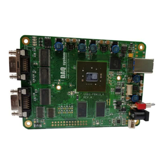
USB3-FRM13_K Users Manual (Rev 1.1) 3. USB3-FRM13_K Description In this chapter, the primary functions of the board are described briefly. For more information, refer to the device specification. 3.1 USB3-FRM13_K Layout [Figure 3-1. USB3-FRM13_K Layout] The board has 6 LEDs to indicate the operation status. : turns on when power is applied to the board and the initialization ends up. -
Page 16: Functional Blocks
USB3-FRM13_K Users Manual (Rev 1.1) 3.2 Functional Blocks (1) MDR-26 Connecter : J1, J2 Camera Link Base (J1), medium/Full (J2) Signal Connector (2) LVDS Link : U2, U3, U4 It is protected a circuit that the interface of high voltage higher than 3.3V CMOS Logic is exchanged to normal 3.3V Logic Level. -
Page 17: Connector Pin-Out
USB3-FRM13_K Users Manual (Rev 1.1) 3.3 Connector Pin-out The board has several connectors and jumpers to set. The USB3-FRM13_K board is equipped with two main connecters, USB3 B-type connector for USB connection and Camera Link connecter for Base/Medium/Full Camera Link connection. The board has several Jumpers for external I/O and Image acquisition. -
Page 18: J1(Mdr26) Connecter
USB3-FRM13_K Users Manual (Rev 1.1) 3.3.2 J1(MDR26) Connecter Figure [3-3] shows the board’s J1 connector pin-map. All of the pin functions are based on the Camera link standard, so please refer to the Camera link standard document for more description and information. Frame Grabber PoCL(+12V) Inner shield... - Page 19 USB3-FRM13_K Users Manual (Rev 1.1) [Table 4. J1 Connector Description] Signal Name Description Remark PoCL_Pin Power over Camera Link(+12V) CC4- Camera Control output 4- CC3+ Camera Control output 3+ CC2-- Camera Control output 2- Camera Control output 1+ CC1+ Serial to Frame grabber + SerTFG+ SerTC- Serial to Camera-...
-
Page 20: J2(Mdr26) Connecter
USB3-FRM13_K Users Manual (Rev 1.1) 3.3.3 J2(MDR26) Connecter Figure [3-4] shows the board’s J2 connector pin-map. All of the pin functions are based on the Camera link standard, so please refer to the Camera link standard document for more description and information. Frame Grabber Inner shield Inner shield... - Page 21 USB3-FRM13_K Users Manual (Rev 1.1) [Table 5. J4 Connector Description] Signal Name Description Remark Inner Shield Cable shield Z3+- Camera link LVDS receive data11+ ZCLK+ Camera link LVDS receive clock+ Z2+- Camera link LVDS receive data10+ Camera link LVDS receive data9+ Camera link LVDS receive data8+ TERMI- Serial to Camera-...
-
Page 22: J3 Connecter
USB3-FRM13_K Users Manual (Rev 1.1) 3.3.4 J3 Connector J3 of the input and output connectors support the Isolated Photo-coupler input signals of four pairs and four TTL Input, two TTL Output signal line. [Figure 3-5. J3 Connector (Top View)] [Table 6. J3 PIN-OUT Description] Signal Name Description N.C. -
Page 23: J8 Connecter
USB3-FRM13_K Users Manual (Rev 1.1) 3.3.5 J8 Connecter It is an external 12V DC Jack power connector DC-005 (2.0) standard. If the USB power is insufficient, you can program does not come out video or down. If the power is insufficient, it will use this connector. 1.0A [Figure 3-6. -
Page 24: Installation
USB3-FRM13_K Users Manual (Rev 1.1) 4. Installation After unpacking, inspect the board to make sure there are no damages on the package. 4.1 Package Contents Product Contents 1. USB3-FRM13_K Board 2. USB3(A-B) Cable 3. CD (Driver/Manual/API/Samples etc.) 4.2 Installation Sequence To install USB3-FRM13_K board in your environment, do the following steps. - Page 25 USB3-FRM13_K Users Manual (Rev 1.1) The item “USB 3.0 Root Hub” should be shown in the “Device Manager” window as shown in [Figure 4-1]. After checking the PC environmental conditions for USB3-FRM13_K, do the following steps to install the board (1) Install the USB3-FRM13_K board into your system.
- Page 26 USB3-FRM13_K Users Manual (Rev 1.1) [Figure 4-3. Specify the driver folder] Select “Search for the best driver in these locations”. Check “Search removable media (floppy, CD-ROM)”. Check “include this location in the search”. Click “Browse” button. Select the folder where the drivers are located. Click “OK”. Click “Next”. The necessary files are “cyusb3.inf”...
- Page 27 USB3-FRM13_K Users Manual (Rev 1.1) [Figure 4-4. Warning window] When you across a window’s warning message regarding to the compatibility problem as shown the [Figure 4-4] during the installation process, just click “Continue” button and go on the installation. http://www.daqsystem.com...
- Page 28 USB3-FRM13_K Users Manual (Rev 1.1) If the installation is completely finished, a completion window message shall be shown as in [Figure 4-5]. Click “Finish”. [Figure 4-5. “Completion” message window] http://www.daqsystem.com...
- Page 29 13 Device” in the “Device Manager” window as shown in [Figure 4-6]. [Figure 4-6. “Device Manager” window] If you can see the “DAQ system USB3.0 Frame 13 Device” at the Universal Serial Bus controllers, the driver installation is to have been over. (Check the red circle)
-
Page 30: Sample Program
USB3-FRM13_K Users Manual (Rev 1.1) 5. Sample Program DAQ system provides a sample program to make the user be familiar with the board operation and to make the program development easier. You can find the sample program in the CDROM accompanying with the board. -
Page 31: Image Functions
USB3-FRM13_K Users Manual (Rev 1.1) (Notice) The running order for the sample program as “Device Open” click “Device Init” click Select Mode “8, 16, 32, 64” Get Resolution “Start” click “View” Click or “Auto” check 5.1 Image Functions (1) “Open”... - Page 32 USB3-FRM13_K Users Manual (Rev 1.1) (9) “Data” button Press this button to read the image frame data of the board to your PC(Hex Value). If image frame data is not saved on the board, you must wait until the end of data collection. (10) “Auto”...
- Page 33 USB3-FRM13_K Users Manual (Rev 1.1) (14) “6 tap” toggle Test function for DAQ system. (15) “Full screen” toggle It shows full screen. (16) ”R/B Change” toggle The image color can be changed (Red <-> Blue). (17) “use DVAL” toggle If the box clicks, you use the Data Valid signal.
-
Page 34: Multi-Board Functions
USB3-FRM13_K Users Manual (Rev 1.1) (21) “Auto Save” toggle If you click the box, the video data is saved as a BMP, JPG (x86), Binary (Hexa value) file in the frame unit in Saved (or the folder selected by the user: Select Folder) specified below. In the case of JPEG, it does not work in 64-bit O.S. - Page 35 USB3-FRM13_K Users Manual (Rev 1.1) (2) “Data(CC)Out” button Write the CC(Camera Control) data. (3) Clear Error Error number is initialized to “0”. “Suce: Success” : It shows good image transfer state. “Fail” : It shows bad image transfer state. OE : Overflow Error UE : UnRead Error SE : Size Error Size...
-
Page 36: Trigger Configure Functions For Line Scan Camera
USB3-FRM13_K Users Manual (Rev 1.1) (4) “UART Send” button Send the UART data. (5) “UART Get” button Get the data from UART buffer. (6) “UART Clear” button Clear the UART Receiver buffer. 5.5 Trigger Configure Functions for :Line Scan Camera (1) “Data(CC)Out”... - Page 37 USB3-FRM13_K Users Manual (Rev 1.1) (4) “# of Line” button It is a Line number, you can select 1 ~ 65536. (5) “CC Cfg” button You can select a CC(camera control) signal among CC1 ~ CC4. Camera Option can be selected from Camera Control signal lines (cc1 alt ~ cc4 alt). If you select “cc1 alt”...
- Page 38 USB3-FRM13_K Users Manual (Rev 1.1) (7) “Use Ext, Ref, Clock” toggle If the button clicks, you can use an external reference clock. (8) “Configure Trigger” button Trigger # 1 (CC1), Trigger # 2 (CC2) of the following conditions, is set depending on the selected trigger Delay, Width, Blank.
- Page 39 USB3-FRM13_K Users Manual (Rev 1.1) Delay Width Blank Trigger Clock Increasing the Width increases the width of the pulse, and increasing the Blank increases the gap. Delay Width Blank Trigger Clock For example, if you want 5MHz trigger clock at the CC1 or CC2 , you set the CC that you want at the “CC Cfg”...
- Page 40 USB3-FRM13_K Users Manual (Rev 1.1) Trigger Clock Delay Width Blank (9) Trigger Line Mode Selection The trigger starts the below selected method. Continuous --- Free Run Mode. It is used an internal 50MHz clock.. Line trig --- It is used a Line Trigger Mode. A Phase --- It is used an A –Phase.
- Page 41 USB3-FRM13_K Users Manual (Rev 1.1) (10) “Ext. Inverse”: When selected, the external trigger waveform is inversely converted and input. “Ext. Enable”: When selected, external trigger mode On/Off is executed. “ENC A Inv.” : When selected, the waveform of encoder A is converted and input. “ENC B Inv.”...
-
Page 42: Appendix
USB3-FRM13_K Users Manual (Rev 1.1) Appendix A.1 Specification Supply PoCL 12V 330mA 10V 400mA External Digital Input/Output Characteristics Number of Digital I/O Lines 4-pair Differential Input 4 TTL Input 2 TTL Output Clocks Pixel Clock Frequency Range : 20MHz to 85MHz Caution) A Camera link specification is the minimum clock is 20MHz. - Page 43 USB3-FRM13_K Users Manual (Rev 1.1) Serial Interface (Option) 8bit Data, 1 Stop bit, No parity Baud Rates --- 9600, 19200, 38400, 57600, 115200 Power Requirement Voltage : +3.3V (Max. 500mA) +12V (Max. 1A) Physical Characteristics Camera Interface : Camera Link 1.1 ...
-
Page 44: Physical Dimension
USB3-FRM13_K Users Manual (Rev 1.1) A.2 Physical Dimension The approximate external dimensions of the board are as follows. For more detailed measurements, ask the person in charge. http://www.daqsystem.com... - Page 45 1. USB 3.0 System Architecture -- Don Anderson, USB SIG(www.usb.org) 2. Universal Serial Bus Specification -- Compaq/Intel/Microsoft/NEC, MindShare Inc. (Addison Wesley) 3. AN201 How to build application using API -- DAQ system 4. AN342 USB3-FRM13_K API ver1.0 -- DAQ system http://www.daqsystem.com...
Need help?
Do you have a question about the USB3-FRM13-K and is the answer not in the manual?
Questions and answers