Table of Contents
Advertisement
Quick Links
USB3-FRM20
User Manual
Version 1.1
ⓒ 2005 DAQ SYSTEM Co., Ltd. All rights reserved.
Microsoft® is a registered trademark; Windows®, Windows NT®, Windows XP®, Windows 7®, Windows 8®, Windows 10®
All other trademarks or intellectual property mentioned herein belongs to their respective owners.
Information furnished by DAQ SYSTEM is believed to be accurate and reliable, However, no responsibility is assumed by DAQ SYSTEM for its use, nor
for any infringements of patents or other rights of third parties which may result from its use. No license is granted by implication or otherwise under
any patent or copyrights of DAQ SYSTEM.
The information in this document is subject to change without notice and no part of this document may e copied or reproduced without the prior
written consent.
Advertisement
Table of Contents

Subscribe to Our Youtube Channel
Related Manuals for DAQ system USB3-FRM20


Summary of Contents for DAQ system USB3-FRM20
- Page 1 All other trademarks or intellectual property mentioned herein belongs to their respective owners. Information furnished by DAQ SYSTEM is believed to be accurate and reliable, However, no responsibility is assumed by DAQ SYSTEM for its use, nor for any infringements of patents or other rights of third parties which may result from its use. No license is granted by implication or otherwise under any patent or copyrights of DAQ SYSTEM.
-
Page 2: Table Of Contents
USB3-FRM20 User’s Manual Contents 1. Introduction 1-1. Product Specification ------------------------------------------------------------------------ 1-2. Product Application ------------------------------------------------------------------------ 2. USB3-FRM20 Description 2-1. Layout ------------------------------------------------------------------------ 2-2. Board Description ------------------------------------------------------------------------ 2-3. I/O Terminal Pin Map ------------------------------------------------------------------------ 2-4. Board Size ------------------------------------------------------------------------ 3. Sample Program ------------------------------------------------------------------------ 3-1. Description of Image Frame Functions ------------------------------------------------------- 3-2. -
Page 3: Introduction
USB3-FRM20 User’s Manual 1. Introduction 1-1. Product Specification Item Description Remark Hardware PC Interface USB3.0 B-Type Operation Power +12VDC/650mA External 12V DC Power (A6-Type : 5.5x2.1mm) Video Interface MIPI CSI C-PHY 3 Lane 2.2 ~ 2.3 Gsym / 1 Lane MIPI CSI D-PHY 4 Lane 2.5Gbps / 1 Lane... -
Page 4: Product Application
- Frame Grabber - Test for Variable MIPI Sensor The USB3-FRM20 board transmits the C-PHY or D-PHY MIPI (Mobile Industry Processor Interface) signal of the sensor board to the PC in the USB3.0 Super Speed (5Gbps) method. Two signals of C-PHY or D-PHY can be selected and used. The received signal is processed by the software (application) provided by the DAC system in the PC and displayed as an image. -
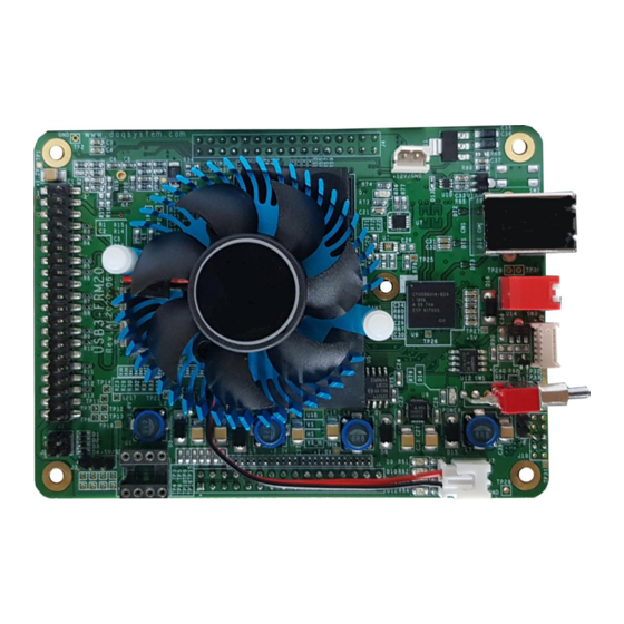
Page 5: Usb3-Frm20 Description
123 789 REF1 REF2 [Figure 2-1. USB3-FRM20 Components Layout] There are 6 important LEDs on the board, and the description of each is as follows. : Lights up when the board is configured and ready for operation. : Lights up when connected via USB3.0 (blinks). -
Page 6: Board Description
USB3-FRM20 User’s Manual 2-2. Board Description As shown in the figure below, in the case of USB3-FRM20, the overall control is in charge of FPGA Core Logic. Its main function is to transmit C-PHY or D-PHY MIPI Image Frame Data signals through the External I/O connector. -
Page 7: I/O Terminal Pin Map
USB3-FRM20 User’s Manual 2-3. I/O Terminal Pin Map (1) USB3.0 B type CN1 connector When the PIN of the USB3.0 Standard Powered-B type connector of the board is viewed from the front where the cable is connected, it is as shown in [Figure 2-3]. - Page 8 USB3-FRM20 User’s Manual [Table 2. J1 Connector Description] Name Description Remark SENSOR Power SENSOR Power SENSOR Power SENSOR Power Ground Ground Serial Clock C_L0_RXA or D_L0_RXP C_lane0_RX_A or D_lane0_RX_P C : C-Phy, D : D-Phy Serial Data C_L0_RXB or D_L0_RXN...
- Page 9 USB3-FRM20 User’s Manual SENSOR Power SENSOR Power (3) J2 It is a connector used as SPI (Serial Peripheral Interface). [Figure 2-5. J5 Connecter (Top View)] [Table 3. J2 Connecter Description] Name Description F_SPI_SCK Serial Clock F_SPI_SSN Slave Select F_SPI_MISO Master Input, Slave Output...
- Page 10 USB3-FRM20 User’s Manual PWR_SDA Power Serial Data AD_SCL AD Serial Clock To be updated AD_SDA AD Serial Data To be updated Ground Ground OS_SCL OS Serial Clock To be updated OS_SDA OS Serial Data To be updated P_GPIO8 General Purpose IO8...
- Page 11 USB3-FRM20 User’s Manual SPI_CLK SPI Clock SPI_MOSI SPI Master Out Slave In SPI_EN SPI Enable SPI_MISO SPI Master In Slave Out 5V_IN 5V Power V_IO2 IO2 Power P_GPIO0 General Purpose IO0 P_GPIO1 General Purpose IO1 P_GPIO2 General Purpose IO2 P_GPIO3...
- Page 12 USB3-FRM20 User’s Manual (8) SW3 The USB3-FRM20 board is designed to use up to 4 USB3-FRM20 boards simultaneously in one system (PC). Classification of each board can be set through a 2-pin DIP switch in the board. [Figure 2-9. SW3 switch (Top View)] [Table 6.
-
Page 13: Board Size
USB3-FRM20 User’s Manual 2-4. Board Size The external dimensions of the board are as follows. (For detailed dimensions, please ask the person in charge.) < Top View > 15.5 10.7 < Right Side View >... -
Page 14: Sample Program
USB3-FRM20 User’s Manual 3. Sample Program A sample program is provided on the CDROM provided with the board so that the board can be used easily. In order to test the sample program, the driver of the board must be installed first. The sample program is provided in the form of a source so that the API provided to use the board can be briefly tested, so the user can modify and use it. -
Page 15: Description Of Image Frame Functions
USB3-FRM20 User’s Manual All files specified above are included on the supplied CDROM. In order to run the sample program normally, API DLL (USB-FRM20.DLL) must be in the folder of the executable file, or in the Windows system folder or the folder designated by the Path environment variable. - Page 16 USB3-FRM20 User’s Manual (7) “S-Read” button The sensor initialization file is read from the program. Depending on the address_data size (8_8, 16_8, 16_16) of the above command, it is possible to send commands to the INI file at a time or use the command line by line by I2C read/write. The structure and description of the ini file are as follows.
- Page 17 USB3-FRM20 User’s Manual 0x5405 80 0x540c 05 0x5b00 00 0x5b01 00 0x5b02 01 0x5b03 ff 0x5b04 02 [END] (8) “Init” button Initialize the sensor by selecting “INI, T1, T2, SPI” below. (To be added) (9) “Go/Stop” toggle button Initialize the sensor and read INI at once.
- Page 18 USB3-FRM20 User’s Manual (15) “Data” button The image frame saved on the board is read into PC (Hexa value). If the image frame is not saved on the board, you have to wait until the saving is complete. Use after freeze the screen.
-
Page 19: Description Of Clock Functions
USB3-FRM20 User’s Manual (19) “YUV; RGB; RAW; USER” : User setting or image input format selection “No Skip” : No Skip “5’th Skip” : When selected, the 5th byte is skipped. For example, if the input data is Bayer with 10 bits, 8 bits each is stored in the 5th byte each of the remaining 1 bit excluding RGB and 3 bytes and 1 byte. -
Page 20: Description Of Power/Digital I/O Functions
USB3-FRM20 User’s Manual (4) “Set 16M” button Set MCLK(Master Clock) to 16MHz. (5) “A/CHG” toggle If checked, the interval of the frequency set by Min. and Max. can be periodically set and tested according to the Step. Example) In the above case, the frequency increases between 5 and 30 MHz in units of 0. -
Page 21: Description Of I2C Read/Write Functions
USB3-FRM20 User’s Manual 3.4 Description of I2C Read/Write Functions (1) “Init” button Initialize the I2C registers. (2) “Write” Button Send data through I2C. (3) “Read” Button Reads the data of the address of the selected mode among SYS, PWR, ADC, and OS modes below. -
Page 22: Description Of Misc. Functions
USB3-FRM20 User’s Manual “ADC” : AD Converter “OS” : Open Short 3.5 Description of Misc. Functions Various types of conditions can be selected and used. “+5V Power” : Outputs VIO power. ”I/O Power” : Turns on/off the power of external signals used for MIPI. -
Page 23: Description Of Status Functions
USB3-FRM20 User’s Manual 3.6 Description of Status Functions “SP0..5 Setup” : SP0..3 (Sensor Power) voltage (0.9 ~ 4.1V) can be controlled. “Log Enable” : Log On/Off “Data Check” : If checked, the previous image data (saved image) and the current image data are compared and the value of the wrong part is displayed on the left log screen at the bottom. -
Page 24: Appendix
USB3-FRM20 User’s Manual Appendix A-1. MIPI-PWR02 Power Board 1. J1 Connector (2x20 Pin Right Angle Type) It is connected to the power and the signal is as follows. 25 27 [Figure 1. J1 Connector (Top View)] [Table 1. J1 Connector Description 설명]... - Page 25 Caution) 1 ~ 1.5A in total of SP0 ~ SP5 2. J2 Connector It is connected to USB3-FRM20 board J4, and is a connector related to sensor power and some GPIOs (General Purpose In/Out). (Refer to Section 2.3 J4 Connector) 3.
-
Page 26: A-2. Repair Regulations
⑥ Products whose serial number has been changed or deliberately removed ⑦ If DAQ SYSTEM determines that it is the customer's fault due to other reasons (5) Customer is responsible for shipping costs for returning the repaired product to DAQSYSTEM. - Page 27 USB3-FRM20 User’s Manual MEMO Contact Point Web sit : https://www.daqsystem.com Email : postmaster@daqsystem.com...
Need help?
Do you have a question about the USB3-FRM20 and is the answer not in the manual?
Questions and answers