Table of Contents
Advertisement
Quick Links
Quadruple Output Regulator with Two High-Side Switches,
Features and Benefits
• Four independent, high current switching regulators
• Adjustable 1.0 A/±1.5% always-on asynchronous buck
regulator with an integrated 150 mΩ MOSFET (SW1)
▫ Employs PFM to deliver 3.3 V/40 µA while drawing less
than 50 µA from V
of 12 V
IN
▫ Operates down to at least 3.6 V
• Adjustable 1.5 A/±1.5% asynchronous buck regulator with
an integrated 120 mΩ high-side MOSFET (SW2)
• Adjustable 2.0 A/±1.5% asynchronous buck regulator with
an integrated 110 mΩ MOSFET (SW3)
• Adjustable ±1.5% synchronous buck controller with
integrated gate drivers and current sensing (SW4)
• Fixed 425 kHz, interleaved PWM switching frequency
• EN/SYNC input for PWM frequency scaling
• Adjustable soft-start time for each switching regulator
• All switching regulators provide prebias startup with zero
reverse current
• All switching regulators have overvoltage protection
• External compensation for all switching regulators
Continued on the next page...
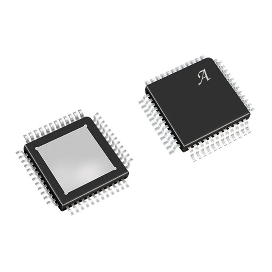
Package: 48-pin LQFP (suffix JP)
Not to scale
A8600-DS, Rev. 4
BU/ACC Voltage Detectors, and Mute Delay
IN
Switcher 1
Switcher 2
(SW1)
(SW2)
Adjustable
Adjustable
Output Voltage
Output Voltage
1.0 A
/ 2.5 A
1.5 A
/ 2.5 A
AVG
PEAK
AVG
Always-On
PWM / PFM
PWM
Asynchronous
Asynchronous
Buck
Buck
Regulator
Regulator
Charge
Pump
Enable and
Synchronization
(EN/SYNC)
425 kHz
180° Shift
Figure 1. A8600 major features
Description
Designed to provide the power supply requirements of next
generation car audio and infotainment systems, the A8600
provides all the control and protection circuitry to produce
four high current regulators, each with ±1.5% accuracy. The
A8600 includes control circuitry to implement three adjustable,
asynchronous buck regulators with integrated MOSFETs. Also,
the A8600 provides the control circuitry, gate drivers, and
current sensing to implement a synchronous buck controller
with external MOSFETs. In standby mode, the A8600 draws
less than 50 µA from V
frequency modulation (PFM) to deliver 3.3 V/40 µA via the
always-on regulator, SW1. The always-on regulator operates
down to at least V
Features of the A8600 include: an EN/SYNC input to either
turn the A8600 on/off or increase/decrease the base pulse
width modulation (PWM) frequency, four adjustable soft-start
times, and four external compensation pins. Output voltage
monitoring of switchers SW2, SW3, and SW4 is provided
by a single, open-drain POK output. In addition, the A8600
provides two high voltage, high-side switches with foldback
overcurrent protection. These two high-side switches actively
block reverse current. The A8600 also provides direct battery
(BU) and switched (accessory) battery (ACC) detectors and
a mute pulse output with an adjustable delay.
Continued on the next page...
Switcher 3
(SW3)
Adjustable
Output Voltage
Output Voltage
2.0 A
/ 2.5 A
PEAK
AVG
PEAK
PWM
Asynchronous
Buck
Regulator
High-Side Switch 1
BU and ACC
(S1)
Detectors
1.0 Ω Total
with
Foldback Limiting
High-Side Switch 2
(S2)
Mute Pulse
1.0 Ω Total
with Delay
with
Foldback Limiting
of 12 V while employing pulse
IN
of 3.6 V (V
falling).
IN
IN
Switcher 4
(SW4)
Adjustable
Adjustable I
LIM
PWM
Synchronous
Buck
Controller
A8600
Advertisement
Table of Contents

Subscribe to Our Youtube Channel
Summary of Contents for Allegro MicroSystems A8600
- Page 1 • Fixed 425 kHz, interleaved PWM switching frequency • EN/SYNC input for PWM frequency scaling Features of the A8600 include: an EN/SYNC input to either • Adjustable soft-start time for each switching regulator turn the A8600 on/off or increase/decrease the base pulse •...
- Page 2 (S1 and S2) with foldback short circuit protection The A8600 is supplied in a low profile 48-pin LQFP package (suffix • High-side switches simultaneously controlled on/off JP ) with exposed power pad. It is lead (Pb) free, with 100% matte- •...
-
Page 3: Table Of Contents
A Generalized Tuning Procedure Power Dissipation and Thermal Calculations Current Sense Amplifiers PCB Component Placement and Routing Power MOSFETs Pin Descriptions Table BOOT Regulators Pin ESD Structures Package Outline Drawing Allegro MicroSystems, LLC 115 Northeast Cutoff Worcester, Massachusetts 01615-0036 U.S.A. 1.508.853.5000; www.allegromicro.com... -
Page 4: Absolute Maximum Ratings
On 2-layer PCB with 3 in. of copper area on 2 sides ºC/W Package Thermal Resistance, ºC/W θJP Junction to Pad *Additional thermal information available on the Allegro website. Allegro MicroSystems, LLC 115 Northeast Cutoff Worcester, Massachusetts 01615-0036 U.S.A. 1.508.853.5000; www.allegromicro.com... - Page 5 Feedback pin for buck regulator SW1 VINS S1/S2 high-side switch input Feedback pin for buck regulator SW2 VREG Internal voltage regulator bypass capacitor pin Feedback pin for buck regulator SW3 Allegro MicroSystems, LLC 115 Northeast Cutoff Worcester, Massachusetts 01615-0036 U.S.A. 1.508.853.5000; www.allegromicro.com...
-
Page 6: Typical Application Circuit
Current will not flow from ACCO, BUO, MUTE, BIAS, VREG, FB1, POK, or OUTx to any VINx pin SW4 lower FET must not cause V to decay during prebias startup Allegro MicroSystems, LLC 115 Northeast Cutoff Worcester, Massachusetts 01615-0036 U.S.A. - Page 7 S W2 and S W3 only FBx OV 860mV POKx GLITCH FBx UV 740mV S W2 & S W3 only Figure 2. Detailed functional block diagram for SW1, SW2, and SW3 Allegro MicroSystems, LLC 115 Northeast Cutoff Worcester, Massachusetts 01615-0036 U.S.A. 1.508.853.5000; www.allegromicro.com...
- Page 8 RE S E T DOMINA NT LX4 or FA ULTS SS4 < 0.2V 0.2V FB4 OV 860mV POK 4 GLITCH FB4 UV 740mV Figure 3. Detailed functional block diagram for SW4 Allegro MicroSystems, LLC 115 Northeast Cutoff Worcester, Massachusetts 01615-0036 U.S.A. 1.508.853.5000; www.allegromicro.com...
-
Page 9: Electrical Characteristics Table
Power OK (POK) POK Low Condition Output Voltage = 3 mA − − POKO(L) POK Leakage = 5.0 V −1 − µA POK(LKG) POKO Continued on the next page… Allegro MicroSystems, LLC 115 Northeast Cutoff Worcester, Massachusetts 01615-0036 U.S.A. 1.508.853.5000; www.allegromicro.com... - Page 10 Open Loop Voltage Gain = 1.2 V VOL1 COMP1 400 mV < V μA/V Transconductance 0 V < V < 400 mV μA/V Continued on the next page… Allegro MicroSystems, LLC 115 Northeast Cutoff Worcester, Massachusetts 01615-0036 U.S.A. 1.508.853.5000; www.allegromicro.com...
- Page 11 > 0.3 V − − cycles Hiccup Operation BOOT Shorted − − BOOTUV1 Count cycles Hiccup Operation BOOT Open Count − − BOOTOPEN1 cycles Continued on the next page… Allegro MicroSystems, LLC 115 Northeast Cutoff Worcester, Massachusetts 01615-0036 U.S.A. 1.508.853.5000; www.allegromicro.com...
- Page 12 − − PWMOFFSET2 COMP2 Minimum Controllable On-Time ON(MIN)2 Minimum Switch Off-Time OFF(MIN)2 COMP2 to SW2 Current Gain − − mPOWER2 Slope Compensation mA/μs Continued on the next page… Allegro MicroSystems, LLC 115 Northeast Cutoff Worcester, Massachusetts 01615-0036 U.S.A. 1.508.853.5000; www.allegromicro.com...
- Page 13 > 0.3 V − − cycles Hiccup Operation BOOT Shorted − − BOOTUV2 Count cycles Hiccup Operation BOOT Open Count − − BOOTOPEN2 cycles Continued on the next page… Allegro MicroSystems, LLC 115 Northeast Cutoff Worcester, Massachusetts 01615-0036 U.S.A. 1.508.853.5000; www.allegromicro.com...
- Page 14 − − PWMOFFSET3 COMP3 Minimum Controllable On-Time ON(MIN)3 Minimum Switch Off-Time OFF(MIN)3 COMP3 to SW3 Current Gain − − mPOWER3 Slope Compensation mA/μs Continued on the next page… Allegro MicroSystems, LLC 115 Northeast Cutoff Worcester, Massachusetts 01615-0036 U.S.A. 1.508.853.5000; www.allegromicro.com...
- Page 15 > 0.3 V − − cycles Hiccup Operation BOOT Shorted − − BOOTUV3 Count cycles Hiccup Operation BOOT Open Count − − BOOTOPEN3 cycles Continued on the next page… Allegro MicroSystems, LLC 115 Northeast Cutoff Worcester, Massachusetts 01615-0036 U.S.A. 1.508.853.5000; www.allegromicro.com...
- Page 16 − μA COMP4 Maximum Output Voltage EAO(max)4 Minimum Output Voltage − − EAO(min)4 COMP4 Pull Down Resistance Fault condition − − KΩ COMP4 Continued on the next page… Allegro MicroSystems, LLC 115 Northeast Cutoff Worcester, Massachusetts 01615-0036 U.S.A. 1.508.853.5000; www.allegromicro.com...
- Page 17 SS4 Pull Down Resistance Fault condition − − KΩ SSFLT4 SS4 Startup Current Ratio Relative to I or I −15 − SSSUTRK4 SSSU2 SSSU3 Continued on the next page… Allegro MicroSystems, LLC 115 Northeast Cutoff Worcester, Massachusetts 01615-0036 U.S.A. 1.508.853.5000; www.allegromicro.com...
- Page 18 OUTx ENS High Threshold − − ENSH ENS Low Threshold − − ENSL ENS Hysteresis − − ENSHYS ENS Input Resistance kΩ INENS Continued on the next page… Allegro MicroSystems, LLC 115 Northeast Cutoff Worcester, Massachusetts 01615-0036 U.S.A. 1.508.853.5000; www.allegromicro.com...
-
Page 19: Bu And Acc Comparators
Negative current is defined as coming out of the node or pin, positive current is defined as going into the node or pin. Thermally limited depending on input voltage, duty cycle, regulator load currents, PCB layout, and airflow. Determined by design and characterization, not production tested. Allegro MicroSystems, LLC 115 Northeast Cutoff Worcester, Massachusetts 01615-0036 U.S.A. - Page 20 Quadruple Output Regulator with Two High-Side Switches, A8600 BU/ACC Voltage Detectors, and Mute Delay Figure 4. SW1 PWM Timing Diagram with EN/SYNC pin high Allegro MicroSystems, LLC 115 Northeast Cutoff Worcester, Massachusetts 01615-0036 U.S.A. 1.508.853.5000; www.allegromicro.com...
- Page 21 Quadruple Output Regulator with Two High-Side Switches, A8600 BU/ACC Voltage Detectors, and Mute Delay Figure 5. SW1 Low IQ PWM and Low IP PFM timing, with EN/SYNC low and ACCI low Allegro MicroSystems, LLC 115 Northeast Cutoff Worcester, Massachusetts 01615-0036 U.S.A. 1.508.853.5000; www.allegromicro.com...
- Page 22 Quadruple Output Regulator with Two High-Side Switches, A8600 BU/ACC Voltage Detectors, and Mute Delay Figure 6. SW2, SW3, and SW4 PWM timing Allegro MicroSystems, LLC 115 Northeast Cutoff Worcester, Massachusetts 01615-0036 U.S.A. 1.508.853.5000; www.allegromicro.com...
- Page 23 ENS. reset via EN/SYNC. B. The loads on the A8600 increase and the junction temperature C. The load on one of the high-side switches increases until it begins to increase. When the junction temperature exceeds enters foldback.
- Page 24 Quadruple Output Regulator with Two High-Side Switches, A8600 BU/ACC Voltage Detectors, and Mute Delay Figure 8. BUx, ACCx and MUTE/CTMR timing Allegro MicroSystems, LLC 115 Northeast Cutoff Worcester, Massachusetts 01615-0036 U.S.A. 1.508.853.5000; www.allegromicro.com...
-
Page 25: Functional Description
(decay) time between LXx pulses so the inductor current does pins are held low, SW1 employs pulse frequency modulation not climb to a value that may damage the A8600 or the output (PFM) to draw only 10s of microamperes from the input supply inductor. -
Page 26: Bias Input Pin, Ratings, And Connections
DS(on) performs an analog OR selection between its two positive inputs. The error amplifier regulates either to the soft start pin voltage (minus an offset of 400 mV) or to the A8600 internal reference, 400 mV whichever is lower. To stabilize the regulator, a series RC compensation network... -
Page 27: Boot Regulators
MOSFET pulses to maintain output voltage regulation. (which could be considered to be V In PWM mode all of the A8600 fault detection circuits are active. SW1/2/3/4 Pulse Width Modulation (PWM) See the Timing Diagrams section for diagrams showing how Mode faults are handled when in PWM mode. -
Page 28: Soft Start (Startup) And Inrush Current Control
Soft Start (Startup) and Inrush Current If the voltage at the FB1 pin drops below approximately 800 mV, the A8600 will wake up, and after a delay of approximately 2 µs Control for the IC to fully power-up, turn on the upper MOSFET. V... -
Page 29: Prebiased Startup
13. discharging the output capacitors. As described previously, the If the A8600 is disabled or a fault occurs, the internal fault latch error amplifier usually becomes active when the voltage at the is set and the Soft Start pin is discharged via approximately 5 kΩ. - Page 30 VINS) through the switches. S1 and S2 are simultaneously capacitive load (> 20 A) and the A8600 may have been damaged controlled on or off by the ENS pin. The A8600 contains an inter- or caused some other system level malfunction, such as UVLO nal charge pump to provide gate drive to S1 and S2.
-
Page 31: Bu And Acc Detectors And Mute Output
ACC detectors. VINS pin is isolated in any way, Allegro recommends adding a The A8600 has an open drain, active low MUTE output with a Schottky diode, DVINS, at the VINS pin as shown in figure 18. programmable on-time. The MUTE output is an open drain out- There are two levels of thermal protection in the A8600. -
Page 32: Protection Features
In this section, a description of Pulse-by-Pulse Overcurrent Protection (OCP) each protection feature is provided, and table 1 summarizes the The A8600 monitors the current in the upper MOSFET and if the protection features and their operation. current exceeds the pulse-by-pulse over current threshold (I LIMx then the upper MOSFET is turned off. -
Page 33: Output Short Circuit (Hiccup Mode) Protection
If OCP Enable Threshold, an OCP counter is enabled. The quantity the short circuit is removed, the A8600 will soft start normally of OCP pulses allowed then depends on the FBx voltage. If V and the output voltage will automatically recover to the required is below 300 mV, only 30 OCP counts are allowed. -
Page 34: Asynchronous Diode Protection
If the LXx pin becomes more negative than SW2/3/4 the POK pin will be pulled low. 1.25 V (typ) for more than 50 ns (typ), the A8600 will protect Second, if a higher external voltage supply is accidently shorted itself to prevent damage. - Page 35 EN/SYNC low* Depends on SW2/3/4 Thermal (TSDH) Pulled low Pulled low Latched off or VREG POR via VIN1 UVLO EN/SYNC low requires a logic low for 15 clock cycles. Allegro MicroSystems, LLC 115 Northeast Cutoff Worcester, Massachusetts 01615-0036 U.S.A. 1.508.853.5000; www.allegromicro.com...
-
Page 36: Application Information
Switcher SW1 16.5 5.23 FBA1 FBB1 24.9 4.75 (kΩ) (kΩ) (pF) 34.8 4.53 52.3 7.2 to 12 40.2 4.42 47.5 4.7 to 8 47.5 4.32 51.1 3.3 to 6 Allegro MicroSystems, LLC 115 Northeast Cutoff Worcester, Massachusetts 01615-0036 U.S.A. 1.508.853.5000; www.allegromicro.com... -
Page 37: Output Inductor (Lswx)
6. In equation 6, V (max) is the maximum continu- become unstable when the duty cycle exceeds approximately 50%. However, the slope compensation in the A8600 is a fixed ous input voltage, such as 18 V (not a surge voltage). value (S ) . -
Page 38: Sw1 Low Iq Pfm Ripple Calculation
800 mA (typ) to 0 A: ripple and, in many cases, reduces the stability of the system. The transient response of the A8600 depends on the number and 800 (mA) × L type of output capacitors. In general, minimizing the ESR of (13) the output capacitance will result in a better transient response. -
Page 39: Input Capacitors (Cinx)
The input capacitors must limit the voltage deviations at the 4 µs and a second PFM pulse will be required, about 300 ns later, VINx pin to something significantly less than the A8600 UVLO as shown in figure hysteresis during maximum load and minimum input voltage. -
Page 40: Asynchronous Diode (Dswx)
There are three requirements for the asynchronous diodes. Soft Start and Hiccup Mode Timing (CSSx) The soft start time of the A8600 is determined by the value of the First, the asynchronous diode must be able to withstand the regu- capacitance on the SSx pin (CSSx). -
Page 41: Sw4 External Mosfet Selections
(25) switching frequency. SSSUx When the A8600 is in hiccup mode, the CSSx capacitor is used Compensation Components (RZx, CZx, CPx) as a timing capacitor and sets the hiccup period. The SSx pin To compensate the system, it is important to understand where... - Page 42 (such as for electrolytic output capacitors), then it should be cancelled by the pole formed by the CPx capaci- First, we will take a look at the power stage of the A8600, the tor and the RZx resistor (discussed and identified later as f output capacitors, and the load resistance.
-
Page 43: A Generalized Tuning Procedure
Figure 27. Bode plot of the complete SW3 system (red curve) Figure 28. Transient recovery comparison for f at 3.8 kHz / 66° and 9 kHz / 57° Allegro MicroSystems, LLC 115 Northeast Cutoff Worcester, Massachusetts 01615-0036 U.S.A. 1.508.853.5000; www.allegromicro.com... -
Page 44: Power Dissipation And Thermal Calculations
BU/ACC Voltage Detectors, and Mute Delay Power Dissipation and Thermal Calculations 2) Calculate the RZx resistor value to set the required system bandwidth (f The power dissipated in the A8600 is the sum of the power dissi- 2� × (36) -
Page 45: Pcb Component Placement And Routing
MOSFET1/2/3 to V = 5 V (about 2.5 nC each), Q is the gate A good PCB layout is critical if the A8600 is to provide clean, charge to drive the external MOSFET to V = 5 V (this must stable output voltages. - Page 46 10) Place the boot strap capacitor (CBOOTx) near the BOOTx A8600 to minimize the size of the LXx polygon. Also, keep low- pin and keep the routing to this capacitor as short as possible.
- Page 47 Loop 3 (Blue): When Q3 is on, current flows from the input supply and input capacitors through the output inductor and into the load. At this time the voltage on the output capacitors will increase. Loop 1 LOAD Loop 3 Loop 2 Figure 29. Example PCB component placement and routing, example shows SW3 Allegro MicroSystems, LLC 115 Northeast Cutoff Worcester, Massachusetts 01615-0036 U.S.A. 1.508.853.5000; www.allegromicro.com...
- Page 48 Feedback pin for buck regulator SW3 FB2 or FB4 COMP3 Error amplifier compensation network for regulator SW3 Ground Soft start programming for regulator SW3 Ground Continued on the next page… Allegro MicroSystems, LLC 115 Northeast Cutoff Worcester, Massachusetts 01615-0036 U.S.A. 1.508.853.5000; www.allegromicro.com...
- Page 49 (or Ground Connect to Ground instead, if also SW3 and SW4 both are not used. Connect to Ground instead, if also S1 and S2 both are not used. Allegro MicroSystems, LLC 115 Northeast Cutoff Worcester, Massachusetts 01615-0036 U.S.A. 1.508.853.5000; www.allegromicro.com...
- Page 50 VINx BOOT4 BOOTx PGND PGND SW1, SW2, and SW3 Power Pins; PGND PGND VIN1, VIN2, VIN3, LX1, LX2, LX3, SW4 Output Pins; BOOT4, HG4, LX4 BOOT1, BOOT2, BOOT3 Allegro MicroSystems, LLC 115 Northeast Cutoff Worcester, Massachusetts 01615-0036 U.S.A. 1.508.853.5000; www.allegromicro.com...
- Page 51 PCB layout tolerances; when mounting on a multilayer PCB, thermal vias at the exposed thermal pad land can improve thermal dissipation (reference EIA/JEDEC Standard JESD51-5) Allegro MicroSystems, LLC 115 Northeast Cutoff Worcester, Massachusetts 01615-0036 U.S.A. 1.508.853.5000; www.allegromicro.com...
- Page 52 Copyright ©2012-2016, Allegro MicroSystems, LLC Allegro MicroSystems, LLC reserves the right to make, from time to time, such departures from the detail specifications as may be required to permit improvements in the performance, reliability, or manufacturability of its products. Before placing an order, the user is cautioned to verify that the information being relied upon is current.
Need help?
Do you have a question about the A8600 and is the answer not in the manual?
Questions and answers