
Related Manuals for ADLINK Technology cPCI-3600 Series


Summary of Contents for ADLINK Technology cPCI-3600 Series
- Page 1 Series ® 3U CompactPCI Processor Blade with AMD Geode™ LX 800 @ 0.9W User’s Manual Manual Rev.: 2.05 Revision Date: June 11, 2008 Part Number: 50-15058-1000 Advance Technologies; Automate the World.
-
Page 2: Revision History
Series Revision History Revision Release Date Description of Change(s) 2.00 2007/10/16 Document Created Revised ETX Module specifications section, 2.01 2007/10/29 corrected RTM connectivity chart, and revised RTM board and face-plate layout figures. Revised ETX Module VGA support information, 2.02... -
Page 3: Preface
Series Preface Copyright 2008 ADLINK TECHNOLOGY INC. This document contains proprietary information protected by copy- right. All rights are reserved. No part of this manual may be repro- duced by any mechanical, electronic, or other means in any form without prior written permission of the manufacturer. - Page 4 Series Using this Manual Audience and Scope The cPCI-3600 Series User’s Manual is intended for hardware technicians and systems operators with knowledge of installing, ® configuring and using CompactPCI single board computers and ETX modules. Manual Organization This manual is organized as follows:...
- Page 5 Series Conventions Take note of the following conventions used throughout this manual to make sure that users perform certain tasks and instructions properly. Additional information, aids, and tips that help users per- form tasks. NOTE: NOTE: Information to prevent minor physical injury, component damage, data loss, and/or program corruption when try- ing to complete a task.
- Page 6 Series Reference Documentation The following list of documents may be used as reference materi- als to support installation, configuration and/or the operation of the cPCI-3600. This list is prepared in alphabetical order (by vendor name, then by document title) for clarity.
- Page 7 Sales & Service: info@adlinktech.com Toll-Free: +1-866-423-5465 Fax No.: +1-949-727-2099 Mailing Address: 8900 Research Drive, Irvine, CA 92618, USA ADLINK TECHNOLOGY CO. LTD. (BEIJING) Sales & Service: market@adlinkchina.com.cn Telephone No.: +86-10-5885-8666 Fax No.: +86-10-5885-8625 Mailing Address: Rm. 801, Power Creative E, No.
- Page 8 Sales & Service japan@adlinktech.com Telephone No. +81-3-4455-3722 Fax No. +81-3-5333-6040 Mailing Address Asahiseimei Hatagaya Bld. 1-1-2 Hatagaya Shibuya-ku, Tokyo, Japan ADLINK TECHNOLOGY INC. (SOUTH KOREA) Sales & Service: korea@adlinkchina.com.cn Telephone No.: +82-2-2057-0565 Fax No.: +82-2-2057-0563 Mailing Address: 4F, Kostech Building, 262-2,...
-
Page 9: Table Of Contents
Functional Block Diagram............ 7 cPCI-3600 CPU (ETX Module) Layout ........ 8 Pin-Out Compatibility ............ 10 cPCI-3600 Series SBC & RTM Connectivity ..... 15 cPCI-3600 SBC (Carrier) Board Layout......17 cPCI-3600 SBC (Carrier) Connectors & Jumpers on Board 19 cPCI-3600 SBC (Carrier) Face-plate Layout ..... 24 cPCI-3600 SBC (Carrier) Connectors on Face-plate.. -
Page 10: Table Of Contents
Series 3 BIOS Settings ..............33 Description ................. 33 Main Menu Setup Items ............. 34 Standard CMOS Features ..........35 Advanced BIOS Features ..........40 Advanced Chipset Features..........43 Integrated Peripherals............45 Power Management Setup ..........48 PnP/PCI Configurations ............. 50 PC Health Status ............... -
Page 11: List Of Figures
Series List of Figures Figure 2-1: cPCI-3600 Series Block Diagram ........7 Figure 2-2: ETX Module Layout Top View ......... 8 Figure 2-3: ETX Module Layout Soldered Side........9 Figure 2-4: Carrier Connector Layout ..........17 Figure 2-5: Carrier Face-plate Layout ..........24 Figure 2-6: RTM Connector Layout.......... - Page 12 Series This page intentionally left blank. List of Figures...
-
Page 13: List Of Tables
Series List of Tables Table 2-1: ETX Module Layout Top View Description ...... 8 Table 2-2: ETX Module Layout Soldered Side Description....9 Table 2-3: X1 Connector: PCI-bus, USB, & Audio......10 Table 2-4: X2 Connector: ISA Bus..........11 Table 2-5: X3 Connector: CRT, LCD (LVDS), &... - Page 14 Series This page intentionally left blank. List of Tables...
-
Page 15: Introduction
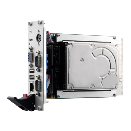
Series Introduction This chapter introduces the cPCI-3600 Series, presents a general overview of its package contents, specifications, features, and applications. 1.1 Overview The cPCI-3600 Series is a state-of-the-art single board computer ® in a 3U dual-slot CompactPCI form factor featuring an extremely energy efficient AMD Geode™... -
Page 16: Package Contents
Series 1.2 Package Contents The cPCI-3600 Series is packaged with the following components. cPCI-3600 SBC (Carrier Board) cPCI-3600 Dual-slot 3U AMD Geode™ LX 800 SBC with dual- USB, dual-COM, and 10/100 LAN ports, PS/2 keyboard and mouse, as well as CRT output. -
Page 17: Specifications
Series 1.3 Specifications cPCI-3600 SBC (Carrier Board) ® Compliant with PICMG 2.0 Rev 3.0 ® CompactPCI Bus 32-bit/33 MHz PCI Bridge: PCI2050 Peripheral Connectivity 44-pin IDE connector on Board ® CompactFlash slot Two USB ports Fast LAN port Two COM ports... - Page 18 Series cPCI-3600 CPU (ETX Module) Embedded Processor: AMD Geode™ LX 800 CPU 500 MHz. Chipset: Geode™ CS5536 companion device Memory: 256 MB of soldered onboard DDR 400 memory and one 200-pin socket for additional, up to 1 GB DDR 400 SODIMM.
- Page 19 Series PIO mode 4, multi-word DMA mode 2 drivers and Ultra DMA-mode 6. USB: supports up to four ports ver 2.0 Audio Chipset: included on CS5536 Audio Codec: AC'97 specification v2.3 compliant interface to multiple audio codecs ® LAN Chipset: Intel...
-
Page 20: Features
EEPROM CMOS Backup USB Boot/Legacy ® ® ® Supports Windows 2000/XP and Red Hat Linux 1.5 Applications The ADLINK cPCI-3600 Series is suitable for: Electronics manufacturing testing Industrial automation and control Military and aerospace Traffic and public transportation system Introduction... -
Page 21: Hardware Information
Series Hardware Information This chapter presents detailed cPCI-3600 Series layout informa- tion, technical drawings, pin-out settings, and jumper settings. 2.1 Functional Block Diagram Figure 2-1: cPCI-3600 Series Block Diagram Hardware Information... -
Page 22: Cpci-3600 Cpu (Etx Module) Layout
Series 2.2 cPCI-3600 CPU (ETX Module) Layout Figure 2-2: ETX Module Layout Top View Table 2-1: ETX Module Layout Top View Description Connector/ Connector/ Description Description Device Device AMD Geode™ LX LAN Controller 800 Processor AMD Geode™ CS5536 SODIMM... -
Page 23: Figure 2-3: Etx Module Layout Soldered Side
Series Figure 2-3: ETX Module Layout Soldered Side Table 2-2: ETX Module Layout Soldered Side Description Connector/ Connector/ Description Description Device Device DDR Soldered Memory BIOS (Optional) ETX Connector ETX Connector (32-bit PCI bus (ISA Bus) USB/Audio) ETX Connector... -
Page 24: Pin-Out Compatibility
Series Pin-Out Compatibility All pins on X1, X2, X3, and X4 of the cPCI-3600 ETX module com- ® ply with pin and signal descriptions used in the original: "ETX Specification ver. 2.6". This document contains a description of pins, signal descriptions, and mechanical characteristics of the ®... -
Page 25: Table 2-4: X2 Connector: Isa Bus
Series Table 2-4: X2 Connector: ISA Bus Signal Signal Signal Signal SD14 SD15 IRQ5 SD13 MASTER# IRQ6 SD12 DREQ7 IRQ7 SD11 DACK7# SYSCLK SD10 DREQ6 SA10 REFSH# DACK6# SA11 DREQ1 DREQ5 SA12 DACK1# MEMW# DACK5# MEMR# DREQ0 SA13 DREQ3... -
Page 26: Table 2-5: X3 Connector: Crt, Lcd (Lvds), & Video
Series Table 2-5: X3 Connector: CRT, LCD (LVDS), & Video Signal Signal First LVDS Channel Signal LVDS Signal LCD0 Txout 0- DDCK LCD1 Txout 0+ DDDA LCD2 Txout 1- LCD16 LCD18 LCD3 Txout 1+ LCD17 LCD19 LCD4 Txout 2-... -
Page 27: Table 2-6: X3 Connector: Com 1/2, Lpt1 Or Fdd, Irda, Mouse, & Keyboard
Series Table 2-6: X3 Connector: COM 1/2, LPT1 or FDD, IrDA, Mouse, & Keyboard Signal Signal Signal LPT/FLPY# RESERVED LPT/FLPY# RESERVED 5VCC 5VCC STB# AFD# RESERVED DENSEL RESERVED RESERVED RESERVED IRRX ERR# IRRX HDSEL# IRTX IRTX RESERVED RXD2 INIT#... - Page 28 Series Table 2-7: X4 Connector: IDE 1, IDE 2, Ethernet, & Miscellaneous Signal Signal Signal Signal S_IOW# P_IOR# 5V_SB PWGIN S_DRQ P_IOW# PS_ON SPEAKER S_D15 P_DRQ PWRBTN# BATT S_D0 P_D15 KBINH LILED# S_D14 P_D0 RSMRST# ACTLED# S_D1 P_D14 ROMKBCS#...
-
Page 29: Cpci-3600 Series Sbc & Rtm Connectivity
Series cPCI-3600 Series SBC & RTM Connectivity Table 2-8: SBC & RTM Connectivity cPCI-3600 (8HP) cPCI-R3600 (8HP) Face-plate Board Face-plate Board Audio (Mic In, Line Out) 44-PIN USB 2.0 Fast LAN Floppy PS/2 KB/MS Reset Button (1) Floppy and LPT ports cannot be used simulta- neously. -
Page 30: Table 2-9: Pci Interrupt Connections
Series Table 2-9: PCI Interrupt Connections PCI slot PCI slot PCI slot PCI slot Onboard interrupt interrupt interrupt interrupt IDSEL Device Pin INTA# Pin INTB# Pin INTC# Pin INTD# cPCI Slot 1 X1_INTAJ X1_INTDJ X1_INTCJ X1_INTBJ AD19 cPCI Slot 2... -
Page 31: Cpci-3600 Sbc (Carrier) Board Layout
Series 2.4 cPCI-3600 SBC (Carrier) Board Layout Figure 2-4: Carrier Connector Layout CNX1 JPY1 Hardware Information... -
Page 32: Table 2-10: Carrier Board Connectors & Jumpers
Series Table 2-10: Carrier Board Connectors & Jumpers Connector/ Connector/ Description Description Jumper Jumper PS/2 KB/MS Clears CMOS CF Master/Slave CF Card Socket Switch VGA Front/Rear IDE Connector JPY1 Switch COM 1 ETX Connector CNX1 COM 2 ETX Connector... -
Page 33: Cpci-3600 Sbc (Carrier) Connectors & Jumpers On Board
Series cPCI-3600 SBC (Carrier) Connectors & Jumpers on Board Table 2-11: CN3: CompactFlash type I/II Signal Name Signal Name SDD3 SDD11 SDD4 SDD12 SDD5 SDD13 SDD6 SDD14 SDD7 SDD15 SDCS#1 SDCS#3 SDIOR# SDIOW# IDEIRQ15 PCSEL SIDERST# SIORDY SDA2 SDA1... -
Page 34: Table 2-12: Cn4: 44-Pin Ide
Series CN4: 44-pin IDE Table 2-12: Signal Name Signal Name Reset IDE IDE Data 7 IDE Data 8 IDE Data 6 IDE Data 9 IDE Data 5 IDE Data 10 IDE Data 4 IDE Data 11 IDE Data 3... -
Page 35: Table 2-13: J1: Compactpci® Pin Assignments
Series ® Table 2-13: J1: CompactPCI Pin Assignments REQ64# ENUM# +3.3V AD [1] V (I/O) AD [0] ACK64# +3.3V AD [4] AD [3] AD [2] AD [7] +3.3V AD [6] AD [5] +3.3V AD [9] AD [8] M66EN C/BE [0]#... -
Page 36: Table 2-14: J2: Compactpci® Pin Assignments
Series ® Table 2-14: J2: CompactPCI Pin Assignments CLK6 LAN82551_TX-P LAN82551_TX-N BRSV CLK5 VGA_HSY_J2 VGA_R_J2 ICMBSDA ICMBSCL ICMBALR BRSV LAN82551_RX-P LAN82551_RX-N VGA_VSY_J2 VGA_B_J2 PRST# REQ6# GNT6# VGA_DDCK_J2 BRSV DEG# VGA_G_J2 VGA_DDDA_J2 FAL# REQ5# GNT5# LAN82551_LINK LAN82551_SPEED LAN82551_ACT X1_SNDL X3_SNDR... -
Page 37: Table 2-15: Jp1: Cmos Selection
Series Table 2-15: JP1: CMOS Selection Jumper Status Normal Clear CMOS Table 2-16: JP2: CF Mode Selection Jumper Status Master Slave Table 2-17: JPY1: VGA Selection Jumper Status Front Panel X1: PCI-Bus, USB, & Audio See section 2.3.2. X2: ISA-Bus See section 2.3.3. -
Page 38: Cpci-3600 Sbc (Carrier) Face-Plate Layout
Series 2.6 cPCI-3600 SBC (Carrier) Face-plate Layout Figure 2-5: Carrier Face-plate Layout cPCI-3600 SBC (Carrier) Connectors on Face-plate Table 2-18: COM 1 & COM 2 (CN6 & CNX1) Pin # RS-232 DCD, Data carrier detect RXD, Receive data TXD, Transmit data... -
Page 39: Table 2-19: Lan: Rj-45 Connector (Cn8)
Series Table 2-19: LAN: RJ-45 Connector (CN8) Signal Function Yellow Red/Green TXDP Transmit Data(+) TXDN Transmit Data(-) Pin 1 RXDP Receive Data(+) Pin 8 LANCT1 Termination LANCT2 Termination RXDN Receive Data(-) LANCT3 Termination LANCT4 Termination Table 2-20: LED Definition... -
Page 40: Table 2-22: Usb 2.0 (Cn5 & Cn7 Right Angle Connector)
Series Table 2-22: USB 2.0 (CN5 & CN7 Right Angle Connector) Signal Name USB- USB+ Ground Table 2-23: VGA/CRT (CN2 Connector) Signal Name Signal Name Green Blue VCC pull-up VCC pull-up DDC2B data HSYNC VSYNC DDC2B clock Hardware Information... -
Page 41: Cpci-3600 Rtm Board Layout
Series 2.8 cPCI-3600 RTM Board Layout Figure 2-6: RTM Connector Layout CNX1 Hardware Information... -
Page 42: Table 2-24: Rtm Board Connectors & Jumpers
Series Table 2-24: RTM Board Connectors & Jumpers Connector/ Connector/ Description Description Jumper Jumper Floppy CNX1 FDD/LPT Select Hardware Information... -
Page 43: Cpci-3600 Rtm Connectors & Jumpers On Board
Series 2.9 cPCI-3600 RTM Connectors & Jumpers on Board Table 2-25: CN5: FDD Connector Signal Pin# Signal Ground X3_AFD-L Ground N.C. Ground X3_PD5 Ground X3_PD0 Ground X3_PD6 Ground X3_ACK-L Ground X3_PD7 Ground X3_BUSY-L Ground X3_INIT-L Ground X3_SLIN-L Ground X3_PE... -
Page 44: Table 2-26: Cn7: Lpt Connector
Series Table 2-26: CN7: LPT Connector Pin # Signal Pin# Signal RPSTROBJ X3_AFD-L RPP0 X3_ERR-L RPP1 X3_INIT-L RPP2 X3_SLIN-L RPP3 Ground RPP4 Ground RPP5 Ground RPP6 Ground RPP7 Ground X3_ACK-L Ground X3_BUSY-L Ground X3_PE Ground X3_SLCT-L Ground Table 2-27: JP1: FDD/LPT Selection... -
Page 45: Cpci-3600 Rtm Face-Plate Layout
Series 2.10 cPCI-3600 RTM Face-plate Layout Figure 2-7: RTM Face-plate Layout LINE OUT LAN 2 Hardware Information... -
Page 46: Cpci-3600 Rtm Connectors On Face-Plate
Series 2.11 cPCI-3600 RTM Connectors on Face-plate Table 2-28: Audio Port (PH 1 & PH 2 Connector) Pin # RS-232 Right-Channel Right-Ground Left-Ground Left-Channel Ground All other connectors (LAN, USB 2.0 & VGA), signals and pin-outs are identical to Carrier Face-plate specifications. -
Page 47: Bios Settings
Series BIOS Settings 3.1 Description The cPCI-3600 Series GLX module uses a Phoenix Award PCI/ ISA BIOS ver 6.0 for system configuration. The Award BIOS setup program is designed to provide maximum flexibility in configuring the system by offering various selectable options to meet end-user requirements. -
Page 48: Main Menu Setup Items
Series 3.2 Main Menu Setup Items The main menu includes the following setup categories. Recall that some systems may not include all entries. Standard CMOS Features (see section 3.3) Sets basic system configuration. Advanced BIOS Features (see section 3.4) Sets advanced features available on the system. -
Page 49: Standard Cmos Features
Series 3.3 Standard CMOS Features The main menu includes the following setup categories. Recall that some systems may not include all entries. Date The BIOS determines the day of the week from other date infor- mation. Time The time format is based on the 24-hour military-time clock. For example, 1 P.M. - Page 50 Series IDE HDD Auto-detection: Press Enter Press Enter to auto-detect the HDD on this channel. If detection is successful, it fills the remaining fields on this menu. IDE Primary Master: None/Auto/Manual Selecting 'manual' allows the user to set the remaining fields on this screen. Selects the type of fixed disk.
- Page 51 Series Access Mode: CHS/LBA/Large/Auto Selects the access mode for a hard disk The following options are selectable only if the 'IDE Primary Master' item is set to 'Manual' Cylinder: Min = 0 Max = 65535 Sets the number of cylinders for a hard disk.
- Page 52 Series Drive A The GLX 800 supports one FDD drive. Because the FDD and LPT1 share the same pins on the X3 connector, only one may be used at a time. Either LPT1 or FDD can be enabled in the follow-...
- Page 53 Series Halt On During the Power On Self Test (POST), the computer stops if the BIOS detects a hardware error. The BIOS can be instructed to ignore certain errors during POST and continue the bootup process. The options are as follows: No errors: POST does not stop for any errors.
-
Page 54: Advanced Bios Features
Series 3.4 Advanced BIOS Features This section allows users to configure the system for basic opera- tion. The following features can be selected: system default speed, boot-up sequence, keyboard operation, shadowing, secu- rity, CPU internal cache, and CPU external cache. - Page 55 Series Boot Other Device Enables the BIOS to boot from a second or third device if booting from the first device fails. When dis- abled the BIOS will not attempt booting from alter- native devices. Boot Up Floppy Seek If enabled, the system will search for disk drives during boot up.
- Page 56 Series security is disabled, the system will boot and setup can be accessed. Remote Console Function Enables remote access through POST messages and commands through serial-port access. Remote Console is a character-based terminal applica- tion. It supports either VT100 or ANSI terminals. It does not support graphics or graphical user interfaces.
-
Page 57: Advanced Chipset Features
Series 3.5 Advanced Chipset Features CPU Frequency Selects the CPU frequency. Options: 200 MHz, 333 MHz, 400 MHz, 433 MHz, and 500 MHz Memory Frequency Selects the memory frequency. Options: Auto, 200 MHz, 266 MHz, 333 MHz, and 400 MHz... - Page 58 Series Video Memory Size Selects the video memory size. Options: None/0 MB, 8 MB, 16 MB, 32 MB, 64 MB, 128 MB, and 254 MB Onboard Audio Turns on/of the onboard audio. Onboard USB 2.0 Turns on/of the onboard USB2.0.
-
Page 59: Integrated Peripherals
Series 3.6 Integrated Peripherals OnChip IDE Channel 1 The integrated peripheral controller contains an IDE interface with support for one IDE channel. Master/Slave Drive PIO Mode The four IDE PIO (Programmed Input/Output) fields allow users to set a PIO mode (0 to 4) for each of the four IDE devices that the onboard IDE interface supports. - Page 60 Series IDE DMA Transfer Access Enables/Disables IDE DMA Transfer Access IDE HDD Block Mode Enhances disk performance by allowing multi-sector data trans- fers and eliminates the interrupt handling time for each sector. 82551 Lan Boot ROM Enables/Disables PXE functions. The PXE function allows system boot from a network environment.
- Page 61 Series EPP Mode Select Selects the version of EPP transfer protocol that the parallel port should use. Users may choose the EPP 1.7 or EPP 1.9 version. Generally, EPP 1.9 is the preferred setting because it supports newer EPP 1.9 devices and most EPP 1.7 devices, while offering other advantages such as support for longer cables.
-
Page 62: Power Management Setup
Series 3.7 Power Management Setup ACPI Function Enabled only if the operating system supports ACPI (Advanced Configuration and Power Interface) specifications. Power Management This item allows you to select the type of Power Management: Options: Disabled, Legacy, APM, or ACPI. - Page 63 Series Soft-Off by PWR-BTTN: Configures the power button: Instant-Off: The power button functions as a normal power- on/-off button. Delay 4 Sec: The system is turned off if the power button is pressed for more than four seconds. IRQ Wakeup Events: IRQ1-15: Enables or disables IRQ Wakeup Events.
-
Page 64: Pnp/Pci Configurations
Series 3.8 PnP/PCI Configurations This section describes configuring the PCI (Personal Computer Interconnect) bus system. PCI is a system which allows I/O devices to operate at speeds nearing the speed the CPU itself uses when communicating with its own components. - Page 65 Series assignment fields are cleared, as the BIOS automatically assigns them. IRQ Resources: When controlling resources manually, assign each system interrupt specifically, depending on the type of device (PCI or ISA) using the interrupt. Options: (IRQ´s) PCI device, Reserved (for ISA-Devices).
-
Page 66: Pc Health Status
Series 3.9 PC Health Status Current CPU Temp. Displays the current CPU temperature. Current System Temp. Displays the current system temperature. CPU VCORE, +3.3 V, +5 V Displays the actual voltage levels on the board BIOS Settings... -
Page 67: Important Safety Instructions
Series Important Safety Instructions For user safety, please read and follow all instructions, WARNINGS, CAUTIONS, and NOTES marked in this manual and on the associated equipment before handling/operating the equipment. Read these safety instructions carefully. Keep this user’s manual for future reference. - Page 68 Series Never attempt to fix the equipment. Equipment should only be serviced by qualified personnel. A Lithium-type battery may be provided for uninterrupted, backup or emergency power. RISK OF EXPLOSION IF BATTERY IS REPLACED BY AN INCORECT TYPE. DISPOSE OF USED BATTERIES ACCORDING TO THEIR INSTRUCTIONS.
-
Page 69: Warranty Policy
Series Warranty Policy Thank you for choosing ADLINK. To understand your rights and enjoy all the after-sales services we offer, please read the follow- ing carefully. 1. Before using ADLINK’s products please read the user manual and follow the instructions exactly. When send-... - Page 70 Series 3. Repair service is not covered by ADLINK's two-year guarantee in the following situations: Damage caused by not following instructions in the User's Manual. Damage caused by carelessness on the user's part during product transportation. Damage caused by fire, earthquakes, floods, lightening, pollution, other acts of God, and/or incorrect usage of volt- age transformers.
Need help?
Do you have a question about the cPCI-3600 Series and is the answer not in the manual?
Questions and answers