
Related Manuals for ADLINK Technology cPCI-6841 Series


Summary of Contents for ADLINK Technology cPCI-6841 Series
- Page 1 Series 6U CompactPCI Pentium M Single Board Computers User’s Manual Manual Rev. 2.01 Revision Date: December 21, 2006 Part No: 50-15048-1000 Advance Technologies; Automate the World.
- Page 2 Copyright 2005 ADLINK TECHNOLOGY INC. All Rights Reserved. The information in this document is subject to change without prior notice in order to improve reliability, design, and function and does not represent a commitment on the part of the manufacturer.
- Page 3 Getting Service from ADLINK Customer Satisfaction is top priority for ADLINK Technology Inc. Please contact us should you require any service or assistance. ADLINK TECHNOLOGY INC. Web Site: http://www.adlinktech.com Sales & Service: Service@adlinktech.com TEL: +886-2-82265877 FAX: +886-2-82265717 Address: 9F, No. 166, Jian Yi Road, Chungho City,...
-
Page 5: Table Of Contents
SBC Specifications ........8 I/O Connectivity ............11 Unpacking Checklist ............12 2 Jumpers and Connectors ..........13 cPCI-6841 Series Mechanical Drawings ......14 cPCI-6841 Series Pin Assignments........17 USB Connectors ............17 VGA Connector ............. 17 Ethernet (RJ-45) Connector .......... 18 PS2 Connector ............. - Page 6 CompactPCI J1 Pin Assignment ........27 CompactPCI J2 Pin Assignment ........28 CompactPCI J3 Pin Assignment (optional) ....29 cPCI-6841 Series Switch and Jumper Settings ....30 SW1: Reset Button ............30 JP1: CF Master or Slave Selection ......30 JP3: PMC VIO Selection ..........
-
Page 7: List Of Tables
List of Tables Table 1-1: Power Ratings ............10 Table 1-2: I/O Connectivity Table ..........11 Table 2-1: Ethernet LED Status ..........18 Table 2-2: Switch and Jumper Functions ........ 30 Table 2-3: JP1 Settings ............30 Table 2-4: JP2 Settings ............31 Table 2-5: JP3 Settings ............ - Page 8 List of Tables...
-
Page 9: List Of Figures
List of Figures Figure 1-1: cPCI-6841 Block Diagram ......... 2 Figure 2-1: cPCI-6841 Top View..........14 Figure 2-2: cPCI-6841 and cPCI-6841-2 Front View ....15 Figure 2-3: cPCI-6841-2 Top View ..........16 Figure 3-1: CPU Installation............34 Figure 3-2: Heatsink Installation ..........35 Figure 3-3: Memory Installation .......... -
Page 11: Introduction
Introduction The cPCI-6841 is a 6U CompactPCI single board computer based on the Intel® Pentium® M processor and 855GME/ICH4 chipset. The Pentium® M processor’s operating frequency ranges from 1.3GHz up to 2.0GHz and it comes with 1MB/2MB L2 cache in an FC-mPGA package. -
Page 12: Figure 1-1: Cpci-6841 Block Diagram
Figure 1-1: cPCI-6841 Block Diagram Introduction... -
Page 13: Main Functions
1.1 Main Functions The following sections explain the main functions of the cPCI-6841. CPU Support The cPCI-6841 SBC is designed for the Intel® Pentium® M and Celeron® M Processors. The standard cPCI-6841 SBC comes μ with CPU socket which can be installed with FC-PGA2 package CPU, with the following options: Pentium®... -
Page 14: Gigabit Ethernet Ports
Gigabit Ethernet Ports The cPCI-6841 has two 10/100/1000Mbps Ethernet (GbE) ports. Every port is assigned a unique static MAC Address. Two onboard Intel® 82541GI Gigabit Ethernet controllers provide two Ethernet ports and are implemented on a 32-bit/33 MHz PCI bus. The 82541GI supports IEEE 802.3x compliant flow control and IEEE 802.3ab compliant 10/100/1000 Mbps auto-negotiation. -
Page 15: Watchdog Timer
Watchdog Timer The cPCI-6841 implements a watchdog timer (WDT) using the Winbond W83627HF Super I/O. The programmable I/O port is on address 2E, and the timer can be set for 1 to 255 seconds or 1 to 255 minutes. Easy-programming libraries for DOS and Windows 95/98/NT are included. -
Page 16: Features
1.2 Features Low power consumption, supports Intel® Pentium® M and Celeron® M CPUs from 1.3GHz up to 2.0GHz Low power consumption Intel® 855GME and ICH4 embed- ded chipset, provides longevity for OEM Compliant with PICMG 2.0, R3.0 32-bit/33 MHz CompactPCI interface based on PCI specifi- cations One 32-bit/33 MHz PMC site Two 200-Pin DDR SODIMM sockets support up to 2GB... -
Page 17: Product List
1.3 Product List The cPCI-6841 series products include the following SBCs: cPCI-6841: Pentium® M SBC with PMC slot cPCI-6841-2: Pentium® M SBC with DVI output Introduction... -
Page 18: Specifications
1.4 Specifications cPCI-6841 SBC Specifications CompactPCI Compliancy PICMG 2.0 CompactPCI Rev. 3.0 Form Factor Standard 6U CompactPCI (board size: 233.35mm x 160mm) Single slot width (4TE or 4HP, 20.32mm) CPU/Cache Single Intel® Pentium® M 1.4GHz, 1.6GHz, 1.7GHz, 1.8GHz, 2.0GHz or Celeron® M 1.3GHz Processors with μ... - Page 19 CompactPCI Bus Controller TI PCI-2050 PCI-to-PCI bridge PCI Rev 2.2 compliant Supports 32-bit/33 MHz Graphics Integrated into 855GME Graphics Memory Controller Hub Shared memory, up to 32MB Dual channel display Front panel DVI connector is available on cPCI-6841-2 only Gigabit Ethernet Two 10/100/1000bps Gigabit Ethernet ports GbE ports are implemented through Intel®...
-
Page 20: Table 1-1: Power Ratings
Real -Time Clock and Nonvolatile Memory Built into Intel® 82801DB southbridge RTC Battery-backed memory is used for BIOS configuration Separate 3V coin cell CR2032 battery used for RTC and nonvolatile memory Environment Operating temperature: 0 to 45°C Storage temperature: -40 to 80°C Humidity: 5% to 95% non-condensed Shock: 15G peak-to-peak, 11ms duration, non-operation Vibration:... -
Page 21: I/O Connectivity
I/O Connectivity cPCI-6841 cPCI-6841-2 Function Face- Face- plate Board plate Board Y (DB-9) Y (DB-9) Y (DB-15) Y (DB-15) Y (Combo) Y (Combo) USB2.0 LAN x 2 Y (RJ-45) Y (RJ-45) Y (IDE 1) Y (IDE 1) Y (32-bit/33 MHz) IDE 1 Y (44-pin) Y (44-pin) -
Page 22: Unpacking Checklist
1.5 Unpacking Checklist Check the shipping carton for any damage. If the shipping carton and contents are damaged, notify the dealer for a replacement. Retain the shipping carton and packing materials for inspection by the dealer. Obtain authorization before returning any product to ADLINK. -
Page 23: Jumpers And Connectors
Jumpers and Connectors This chapter illustrates the board layout, connector pin assign- ments, and jumper setings. Users should be familiar with the prod- ucts before use. The following sections are included: cPCI-6841 and cPCI-6841-2 board outline cPCI-6841 and cPCI-6841-2 connectors pin assignments cPCI-6841 and cPCI-6841-2 jumper settings Jumpers and Connectors... -
Page 24: Cpci-6841 Series Mechanical Drawings
2.1 cPCI-6841 Series Mechanical Drawings Figure 2-1: cPCI-6841 Top View Jumpers and Connectors... -
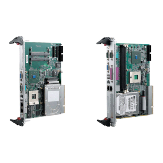
Page 25: Figure 2-2: Cpci-6841 And Cpci-6841-2 Front View
cPCI-6841 cPCI-6841-2 Figure 2-2: cPCI-6841 and cPCI-6841-2 Front View Jumpers and Connectors... -
Page 26: Figure 2-3: Cpci-6841-2 Top View
Figure 2-3: cPCI-6841-2 Top View Jumpers and Connectors... -
Page 27: Cpci-6841 Series Pin Assignments
2.2 cPCI-6841 Series Pin Assignments USB Connectors SIGNAL USB- USB+ Ground VGA Connector Signal Name Pin Pin Signal Name Green Blue N.C. N.C. DDCDAT HSYNC VSYNC DDCCLK Jumpers and Connectors... -
Page 28: Ethernet (Rj-45) Connector
Ethernet (RJ-45) Connector Pin # Signal Name Function LAN_TDP1 Transmit Data1 + LAN_TDN1 Transmit Data1 - LAN_RDP2 Receive Data2 + LAN_RDP3 Receive Data3 + LAN_RDN3 Receive Data3 - LAN_RDN2 Receive Data2 + LAN_TDP4 Transmit Data4 + LAN_TDN4 Transmit Data4 - Left LED Right LED Status... -
Page 29: Ps2 Connector
PS2 Connector Signal Function KBDATA Keyboard Data MSDAT Mouse Data Ground Power KBCLK Keyboard Clock MSCLK Mouse Clock RS-232 Serial Port Connector Signal Name DCD, Data carrier detect RXD, Receive data TXD, Transmit data DTR, Data terminal ready GND, Ground DSR, Data set ready RTS, Request to send CTS, Clear to send... -
Page 30: Dvi Connector
DVI Connector Signal Pin Signal TX2- 16 HTPLG TX2+ TX0- TX0+ I2CCLK I2CDAT VSYNC TXC+ TX1- TXC- TX1+ 26 GREEN BLUE 28 HSYNC Jumpers and Connectors... -
Page 31: Compactflash Connector
CompactFlash Connector Signal Name Pin Pin Signal Name SDD3 SDD11 SDD4 SDD12 SDD5 SDD13 SDD6 SDD14 SDD7 SDD15 SDCS#1 SDCS#3 SDIOR# SDIOW# IDEIRQ15 PCSEL SIDERST# SIORDY SDA2 SDA1 SDDACK# SDA0 IDEACT# SDD0 S66DECT SDD1 SDD8 SDD2 SDD9 IOIS16# SDD10 Jumpers and Connectors... -
Page 32: Floppy Connector
Floppy Connector Signal Name Pin Pin Signal Name Extended Density Data Rate Index Motor A Select Drive B Select Drive A Select Motor B Select Step Direc- tion Step Pulse Write Data Write Gate Track 0 28 Write Protect Read Data Side 1 34 Disk Change Jumpers and Connectors... -
Page 33: Ide Connector
IDE Connector Signal Name Pin Pin Signal Name BRSTDRVJ DDP7 DDP8 DDP6 DDP9 DDP5 DDP10 DDP4 DDP11 DDP3 DDP12 DDP2 DDP13 DDP1 DDP14 DDP0 DDP15 PDDREQ PDIOWJ PDIORJ PIORDY PCSEL PDDACKJ IRQ14 DAP1 DIAG DAP0 DAP2 CS1P CS3PJ IDEACTPJ Jumpers and Connectors... -
Page 34: General Purpose Led Definitions
General Purpose LED definitions Color Status Description IDE idle IDE Media Access IDE access System is not power-on or power failed Power OK Green Power ON User defined General Purpose Blue User defined WDT is not enabled WDT LED Yellow Blinking WDT is enabled Jumpers and Connectors... -
Page 35: Pmc Connector Pin Assignments (Jn1, Jn2)
PMC Connector Pin Assignments (JN1, JN2) Signal Signal Signal Signal Name Name Name Name TCK(3) -12V +12V TRST#(3) INTA# TMS(2) TDO(1) INTB# INTC# TDI(2) BM1(1) INTD# +3.3V BM2(2) +3.3V CLKP1 RST# BM3(3) GNT0# +3.3V BM4(3) REQ0# PME# VIO(4) AD31 AD30 AD29 AD28 AD27... - Page 36 Signal Signal Signal Signal Name Name Name Name VIO(4) EREADY(1) RSTOUT#(1) ACK64# +3.3V REQ64# Monarch#(1) Note 1: These signals are not connected on the board. Note 2: These signals are pulled high on the board. Note 3: These signals are pulled low on the board. Note 4: The VIO signals by default set to +5V via jumper JP3.
-
Page 37: Compactpci J1 Pin Assignment
CompactPCI J1 Pin Assignment REQ64# ENUM#(4) +3.3V AD [1] V (I/O) AD [0] ACK64# GND +3.3V AD [4] AD [3] AD [2] AD [7] +3.3V AD [6] AD [5] +3.3V AD [9] AD [8] M66EN C/BE [0]# GND AD [12] V (I/O) AD [11] AD [10]... -
Page 38: Compactpci J2 Pin Assignment
erate an interrupt when an ENUM# signal is detected. CompactPCI J2 Pin Assignment 22 GND GA4(2) GA3(2) GA2(2) GA1(2) GA0(2) 21 GND CLK6 BRSV(1) BRSV(1) BRSV(1) 20 GND CLK5 BRSV(1) BRSV(1) 19 GND ICMBSDA(1) ICMBSCL(1) ICMBALR(1) GND 18 GND BRSV(1) BRSV(1) BRSV(1) BRSV(1) 17 GND BRSV(1) -
Page 39: Compactpci J3 Pin Assignment (Optional)
CompactPCI J3 Pin Assignment (optional) 19 GND PCIRST-L SIDE_IORDY IDEIRQ15 GND SIDE_DACT- SIDE_66DE 18 GND SIDE_CS-L3 SIDE_CS-L1 17 GND SIDE_D15 SIDE_D14 SIDE_D13 SIDE_D12 SIDE_DAC 16 GND SIDE_D11 SIDE_D10 SIDE_D9 SIDE_D8 SIDE_DRE 15 GND SIDE_A0 SIDE_A1 SIDE_A2 SIDE_IOW- 14 GND SIDE_D7 SIDE_D6 SIDE_D5 SIDE_D4... -
Page 40: Cpci-6841 Series Switch And Jumper Settings
2.3 cPCI-6841 Series Switch and Jumper Settings The following table lists the switch and jumpers on the cPCI-6841 and cPCI-6841V. Switch Function Reset Select CF as Master or Slave Clear CMOS Content PMC VIO Table 2-2: Switch and Jumper Functions SW1: Reset Button SW1 is a push-button on the front panel. -
Page 41: Jp3: Pmc Vio Selection
JP2: Clear CMOS Status 1 2 3 Normal operation (Default) 1 2 3 Clear CMOS Table 2-4: JP2 Settings The CMOS RAM stores the real time clock (RTC) information, BIOS configuration, and default BIOS setting. The CMOS is pow- ered by a button cell battery when the system is powered off. Please use the following procedure to erase the CMOS RAM data: 1. - Page 42 Jumpers and Connectors...
-
Page 43: Getting Started
Getting Started This chapter explains how to install necessary components on the cPCI-6841 and cPCI-6841-2 including: CPU and heat sink Memory module installation HDD installation PMC installation (cPCI-6841 only) CF card installation Main board installation 3.1 CPU and Heatsink The cPCI-6841 and cPCI-6841-2 support the Intel® Pentium® M processor. -
Page 44: Figure 3-1: Cpu Installation
Figure 3-1: CPU Installation Getting Started... -
Page 45: Heatsink Installation
Heatsink Installation Remove the film protecting the thermal pads on the heatsink as shown in Figure 3-2: Heatsink Installation below. Place the heatsink on the CPU and northbride, ensuring that the thermal pads make proper contact with the board components. Secure using the 6 spring-loaded screws provided Figure 3-2: Heatsink Installation Getting Started... -
Page 46: Memory Module Installation
3.2 Memory Module Installation The cPCI-6841 Series SBC provides two 200-pin SODIMM sock- ets for DDR-SDRAM with a maximum memory capacity of 2GB. If memory modules are pre-installed when the package is received, this section may be skipped. The GMCH system memory controller directly supports the follow-... -
Page 47: Pci Mezzanine Card (Pmc) Installation
Figure 3-3: Memory Installation 3.3 PCI Mezzanine Card (PMC) Installation (cPCI-6841 only) The PMC slot is designed for 5V and/or universal PCI interfaces. The PMC site is keyed to prevent users from installing a 3.3V only PMC module. To install the PMC modules: 1. -
Page 48: Figure 3-4: Pmc Installation 1
4. Screw the four PMC mounting bolts to the main board from the bottom side of the SBC to secure the PMC module in place. Figure 3-4: PMC Installation 1 Getting Started... -
Page 49: Hdd Installation On Main Board
Figure 3-5: PMC Installation 2 3.4 HDD Installation on Main Board A slim-type 2.5-inch HDD can be mounted on the cPCI-6841 or cPCI-6841-2. If a HDD is pre-installed, this section may be skipped. 1. Screw the provided standoffs onto the HDD and attach the included 44-pin IDE cable. -
Page 50: Cf Installation (Cpci-6841 Only)
Figure 3-6: cPCI-6841 2.5” Hard Disk Installation 3.5 CF Installation (cPCI-6841 only) The CompactFlash card is widely applied in digital consumer devices such as PDAs, digital cameras and MP3 players. Due to its anti-shock/anti-vibration properties, better environmental toler- Getting Started... -
Page 51: Main Board Installation
ance, low power consumption, small form factor, and high reliabil- ity characteristics, it has been widely accepted in mission critical embedded applications. To install the CF card, insert it into the socket located under the HDD as shown. Figure 3-7: CompactFLASH Card Installation Main Board Installation Use the following procedure to install the cPCI-6841/cPCI-6841-2 main board into a CompactPCI chassis. - Page 52 on the operational purpose of the board. The chassis power may now be turned on. 2. Remove the blank face panel from the slot. 3. Align the top and bottom edges of the board with the card guides on the chassis then slide the board into the chassis until resistance is felt.
-
Page 53: Windows Driver Installation
Windows Driver Installation The following sections show the driver installation procedures for Windows 2000, Windows XP or Windows Server 2003. When installing the Windows drivers, we recommend the following steps: 1. Fully install the Windows properly before installing any driver. Most of the standard I/O devices’ driver will be installed during the standard Windows installation. -
Page 54: Chipset Drivers Installation
4.1 Chipset Drivers Installation 1. Ensure your Windows operating system is fully installed and running prior to executing the “Intel Chipset Soft- ware Installation Utility”. 2. Close any running applications. 3. The files are stored in an integrated application setup program. -
Page 55: Lan Driver Installation
4.3 LAN Driver Installation 1. Boot Windows 2000/XP/Windows Server 2003. 2. Run the pro2kxp.exe under the following directory: X:\cPCI\cPCI-6841\LAN. 3. Read the license agreement. Click 'I accept the terms in the license agreement’ if you agree to continue. 4. At the Location to Save Files prompt, click Next to save the files in the specified folder. - Page 56 Windows Driver Installation...
-
Page 57: Utilities
This section explains the operation of the cPCI-6841’s watchdog timer. The primary function of the watchdog timer is to monitor the cPCI-6841 Series SBC’s operation and to reset the system if the software fails to function as programmed. The watchdog timer can... -
Page 58: Using The Watchdog In An Application
Once the watchdog has timed out, it will cause a RESET signal to be sent to the system. 5.2 Using the Watchdog in an Application The following section is provided to assist you in learning how to use the watchdog in an application. The watchdog’s Reset func- tion is as explained above. -
Page 59: Intel Preboot Execution Environment (Pxe)
5.3 Intel Preboot Execution Environment (PXE) The cPCI-6841 series supports Intel® Preboot Execution Environ- ment (PXE), which provides the capability to boot up or execute an OS installation through an Ethernet connection. There should be a DHCP server in the network with one or more servers running PXE and MTFTP services. - Page 60 Utilities...
-
Page 61: Appendix
Appendix Serial Console User’s Guide 1. Introduction Most industrial implementations do not use a monitor or a key- board to interface between the user and the computer, instead connecting through a network or direct cable. ADLINK provides a function for users to obtain Power-On Self Test (POST) messages and execute commands using serial-port access. -
Page 62: Seting Up The Server
Figure 6-1: Null Modem Connection 3. Seting up the Server The server used in this guide is a CPU board where the Award Preboot Agent is integrated into the BIOS. Use the BIOS setup utility to setup the Serial Console. When you turn on the computer, the Award BIOS is immediately activated. -
Page 63: How To Use The Serial Console
Agent Connect Via This field is un-selectable. Only one connection mode is sup- ported: NULL. NULL means the connection cable is of null modem type. Agent wait time (min) This option selects the amount of time (in minutes) to wait for a successful connection. - Page 64 If your system does not have HyperTerminal installed, please use [Add/Remove Program Properties] in Control Panel to add it. Appendix...
- Page 65 Make sure that HyperTerminal is checked. Appendix...
- Page 66 Select HyperTerminal. Appendix...
- Page 67 Run Hypertrm by double-clicking on the icon. Appendix...
- Page 68 When executing HyperTerminal for the first time, you will be asked to install a modem before running HyperTerminal. Select “No”. Then, you will be asked to enter some configuration settings for your local area. After configuring the basic settings, HyperTerminal will need to build a connection node.
- Page 69 Once you build a connection node, select the serial port that will be used to connect to the server. Appendix...
- Page 70 On the properties page of the chosen serial port, the Bits per sec- ond setting must be the same as the baud rate setting of the server. Before using HyperTerminal to connect to the server, some prop- erties of the console must first be set. Select File --> Properties. Appendix...
- Page 71 Check that the Telnet terminal mode is set to ANSI and select ASCII Setup. Appendix...
- Page 72 To echo the data that the client sends, select all items on the ASCII Setup page. After HyperTerminal is setup and the connection cable is ready, power on the server. POST messages from server will be sent to the HyperTerminal Console as follows. Appendix...
- Page 73 After the server computer boots into the OS, execute commands through the HyperTerminal console as shown. Note: Some keys, (i.e. DEL, ESC, Page Up, Page Down, Up Ar- row, Down Arrow, Left Arrow, Right Arrow) may not be rec- ognized by the server BIOS through the HyperTerminal Appendix...
-
Page 74: Table 6-1: Key Translation Sequences
console. Use the following sequences to perform such ac- tions: Function Key Key Sequence Function Key Key Sequence HOME ESC [ 1 ~ PG UP ESC [ 5 ~ ESC [ 2 ~ PG DOWN ESC [ 6 ~ ESC [ 3 ~ UP ARROW ESC [ A ESC [ 4 ~... -
Page 75: Warranty Policy
Warranty Policy Thank you for choosing ADLINK. To understand your rights and enjoy all the after-sales services we offer, please read the follow- ing carefully. 1. Before using ADLINK’s products please read the user man- ual and follow the instructions exactly. When sending in damaged products for repair, please attach an RMA appli- cation form which can be downloaded from: http:// rma.adlinktech.com/policy/. - Page 76 3. Our repair service is not covered by ADLINK's guarantee in the following situations: Damage caused by not following instructions in the User's Manual. Damage caused by carelessness on the user's part dur- ing product transportation. Damage caused by fire, earthquakes, floods, lightening, pollution, other acts of God, and/or incorrect usage of voltage transformers.
Need help?
Do you have a question about the cPCI-6841 Series and is the answer not in the manual?
Questions and answers