
Subscribe to Our Youtube Channel
Related Manuals for Analog Devices AD9959/PCB


Summary of Contents for Analog Devices AD9959/PCB
- Page 1 (217) 352-9330 | Click HERE Find the Analog Devices AD9959/PCB at our website:...
-
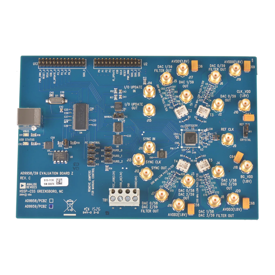
Page 2: Evaluation Board Block Diagram
Information furnished by Analog Devices is believed to be accurate and reliable. However, no responsibility is assumed by Analog Devices for its use, nor for any infringements of patents or other One Technology Way, P.O. Box 9106, Norwood, MA 02062-9106, U.S.A. -
Page 3: Table Of Contents
AD9959/PCB TABLE OF CONTENTS Evaluation Board Block Diagram........... 1 Loading the Software ..............7 Features ....................1 Status Messages upon Loading Software .......8 Applications..................1 Feature Control Windows............9 General Description ................. 1 Chip Level Control..............9 Evaluation Board Hardware ............3 Channel Control..............11 Package Contents................ -
Page 4: Evaluation Board Hardware
AVDD connections allows for the proper functionality of the analog circuitry of all four DACs. Table 2 shows the necessary Analog Devices provides a GUI for the PC; it does not provide connections and the appropriate biasing voltage. control software for external controllers. -
Page 5: Evaluation Board Layout
AD9959/PCB EVALUATION BOARD LAYOUT MANUAL I/O MULTI DEVICE SYNCHRONOUS CONTROL CONTROL CHANNEL 1 CHANNEL 0 HEADERS EVALUATION BOARD CONTROL CLOCK INPUT SUPPLY PORT CLOCK MODE SELECT REF CLK INPUT BAND SUPPLY SDIO RU/RD POWER CONTROL SUPPLY CHANNEL 2 CHANNEL 3 Figure 2. -
Page 6: Evaluation Board Software
AD9959/PCB EVALUATION BOARD SOFTWARE Then, this window (Figure 4) also appears and disappears. INSTALLING THE SOFTWARE Follow these steps to install the AD9959 evaluation software: Log into your PC system with administrative privileges; this is an essential requirement in successfully installing the AD9959 evaluation software. -
Page 7: Windows Xp Users
AD9959/PCB Click Finish after this window (Figure 9) appears. Windows XP Users Power up the AD9959 evaluation board (see Table 2). Connect the evaluation board to the computer using a USB cable via the USB port. Then, the VBUS LED (CR1 on AD9959 evaluation board) illuminates. -
Page 8: Loading The Software
AD9959/PCB After the window in Figure 12 appears, click Finish to exit. LOADING THE SOFTWARE Follow these three steps to load the AD9959 evaluation software: Before starting the software, make sure that the AD9959 evaluation board is powered up, connected to the computer, and that the USB Status LED is flashing. -
Page 9: Status Messages Upon Loading Software
AD9959/PCB Status Messages upon Loading Software Most status message errors can be resolved by checking jumper settings, making sure that the evaluation board is powered up Once the AD9959 evaluation software has been loaded, a green correctly, and inspecting the USB port and cable connections. -
Page 10: Feature Control Windows
AD9959/PCB FEATURE CONTROL WINDOWS Chip Level Control Figure 17. Chip Level Control Window The Chip Level Control window provides control of the Click READ to perform a readback of the current state of the features that affect all channels of the AD9959; this window is settings and update the GUI with those settings. - Page 11 AD9959/PCB CP Current selects the charge pump current output of the Select Use Profile Pins 2 & 3 if you would like to control the PLL in the Ref Clock Multiplier circuitry. Selecting a higher RU/RD feature with Profile Pin 2 and Profile Pin 3, or Use current output will result in the loop locking faster, but there Profile Pin 3 to control this feature using only Profile Pin 3.
-
Page 12: Channel Control
AD9959/PCB Channel Control Figure 21. Channel Control Window The Channel Control window provides control of the features that affect the AD9959 at a channel-specific level. The following describes the sections of the Channel Control window as they are numerically indexed in Figure 21. - Page 13 AD9959/PCB See the DATA LATENCY (PIPELINE DELAY) section in the 7. Output Waveform Specifications table of the AD9959 data sheet for the exact In the Output Waveform box, select either a Cosine(x) or a timing delays with and without this feature enabled. Also, refer Sine(x) function for the angle-to-amplitude conversion.
-
Page 14: Channel Output Config
AD9959/PCB Channel Output Config Figure 23. Channel Output Config Window The Channel Output Config window configures various output The Frequency 00 box also sets the starting point of the linear characteristics of the channel(s). Use the Channel Select tabs to frequency sweep and the first level in frequency modulation (FSK). - Page 15 AD9959/PCB The Enable ASF box also represents the starting point of the Use the Profile Registers to enter the information needed for linear amplitude sweep and the first level in amplitude modulation (FSK, PSK, or ASK) and linear sweep modes of modulation (ASK).
-
Page 16: Debug
AD9959/PCB If we were performing 2-level frequency modulation-no RU/RD, and had the same configurations as shown in Figure 28, P0 would be used to control the modulation on CH0 (see the AD9959 data sheet for more information). Therefore, the output of CH0 will stay at 10 MHz until the P0 button is clicked. -
Page 17: Dut I/O Box
AD9959/PCB DUT I/O Box This dialog box (Figure 32) controls the I/O configuration for the device. Click I/O Reset to send an I/O reset to the corresponding serial port state machine. Select LSB First to change the data format to LSB first from the default setting of MSB first. -
Page 18: Setup Files
AD9959/PCB SETUP FILES Introduction The AD9959 can be configured to perform many operations in various combinations. Preconfigured setup files have been included with the AD9959 evaluation software that show the device in all three modes of operation: single tone, modulation, and linear sweep. These example setup files serve as a reference and/or starting point when trying to configure the device for a desired setup for the first time. -
Page 19: Single Tone Mode
AD9959/PCB Single Tone Mode Open the Single Tone Mode folder to access the single tone mode of operation example setup files. This section discusses the All Channels on @ 10_20_30_40MHz_RURD enabled.stp file. The Chip Level Control window (Figure 37) from this particular setup shows that a 500 MHz System Clock is running, with the RU/RD operation enabled. -
Page 20: Modulation Mode
AD9959/PCB In the Channel Output Config window (Figure 39), Channel 0 has a frequency output of 10 MHz (Frequency 00 box), Channel 1 an output frequency of 20 MHz, Channel 2 an output frequency of 30 MHz, and Channel 3 has a frequency output of 40 MHz. Because the RU/RD operation is enabled, the Enable ASF and Enable Auto ASF boxes are checked. - Page 21 AD9959/PCB The Chip Level Control window (Figure 41) from this particular setup shows that a 500 MHz System Clock is running, and that a 16- level modulation-no RU/RD is being performed. Notice the Level box located in the Modulation Configuration section. The PPC Bit pattern in the Profile Pin Config subsection of the Modulation Configuration is <010>.
-
Page 22: Linear Sweep Mode
AD9959/PCB In the Channel Output Config window (Figure 43), Channel 2 has a frequency output of 3 MHz (Frequency 00 box). When this setup file is loaded, profile pins P1 and P3 are pressed as shown in the Profile and RURD Pin Control Section. In 16-level modulation, P3 is the LSB and P0 is the MSB. - Page 23 AD9959/PCB The Chip Level Control window (Figure 45) from this particular setup shows that a 500 MHz System Clock is running with RU/RD disabled. The Auto Clear Phase Accumulator and Auto Clear Sweep Accumulator boxes have been checked in the All Channel Accumulator Control section to ensure synchronization across channels and reinitialize the starting point once the linear sweep ends.
- Page 24 AD9959/PCB In the Channel Output Config window (Figure 47), all channels (Channel 0 to Channel 3) have an output frequency of 10 MHz (Frequency 00 box). The Enable ASF box is unchecked because a linear amplitude sweep is being performed. The amplitude scalar factor (ASF) is set to 0.5 (half scale), denoting that the sweep begins at half scale and sweeps up to full scale (Amplitude 01-ending point of...
-
Page 25: Schematic
AD9959/PCB SCHEMATIC Figure 48. AD9959/PCB Schematic, Page 1 Rev. 0 | Page 24 of 28... - Page 26 AD9959/PCB Figure 49. AD9959/PCB Schematic, Page 2 Rev. 0 | Page 25 of 28...
- Page 27 0.1µF 0.1µF 2.2µF CLK_VDD AVDD0 AVDD3 0Ω 0Ω 0Ω 0Ω 0Ω 0Ω 0Ω 0Ω 0Ω 0Ω 0Ω 0Ω 0Ω 0Ω 0Ω 0Ω 0Ω 0Ω BG_VDD CLK_VDD BG_VDD Figure 50. AD9959/PCB Schematic, Page 3 Rev. 0 | Page 26 of 28...
-
Page 28: Ordering Information
AD9959/PCB ORDERING INFORMATION ORDERING GUIDE Model Description AD9959/PCB Evaluation Board ESD CAUTION ESD (electrostatic discharge) sensitive device. Electrostatic charges as high as 4000 V readily accumulate on the human body and test equipment and can discharge without detection. Although this product features proprietary ESD protection circuitry, permanent damage may occur on devices subjected to high energy electrostatic discharges. - Page 29 AD9959/PCB NOTES © 2005 Analog Devices, Inc. All rights reserved. Trademarks and registered trademarks are the property of their respective owners. EB05698-0-10/05(0) Rev. 0 | Page 28 of 28...
Need help?
Do you have a question about the AD9959/PCB and is the answer not in the manual?
Questions and answers