Table of Contents
Advertisement
Quick Links
One Technology Way • P.O. Box 9106 • Norwood, MA 02062-9106, U.S.A. • Tel: 781.329.4700 • Fax: 781.461.3113 • www.analog.com
FEATURES
Converts preset standard input frequencies to standard
output frequencies
Input frequencies from 8 kHz to 200 MHz
Output frequencies up to 810 MHz LVPECL and LVDS
(200 MHz CMOS)
Preset pin-programmable frequency translation ratios
On-chip VCO
Single-ended CMOS reference input
2 output clocks (independently programmable as LVDS,
LVPECL, or CMOS)
Single supply (3.3 V)
Very low power: <450 mW (under most conditions)
Small package size: 5 mm × 5 mm
Exceeds Telcordia GR-253-CORE jitter generation, transfer
and tolerance specifications
APPLICATIONS
Cost effective replacement of high frequency VCXO, OCXO,
and SAW resonators
Flexible frequency translation for wireline applications such
as Ethernet, T1/E1, SONET/SDH, GPON, xDSL
Wireless infrastructure
Test and measurement (including handheld devices)
PLEASE SEE THE LAST PAGE FOR AN IMPORTANT
WARNING AND LEGAL TERMS AND CONDITIONS.
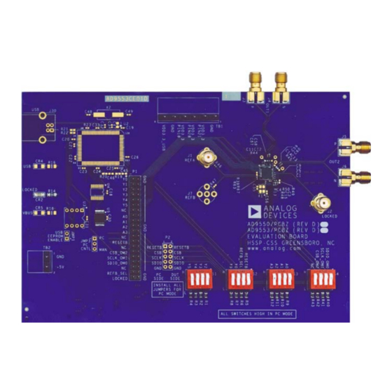
Evaluating the AD9550 Integer-N Clock Translator
DIGITAL PICTURE OF THE AD9550 EVALUATION BOARD
Figure 1. AD9550 Evaluation Board
Evaluation Board User Guide
GENERAL DESCRIPTION
This user guide describes the hardware of the
uation board. The AD9550 evaluation board is a compact,
easy-to-use platform for evaluating all features of the AD9550
integer-N clock translator.
The AD9550 is a phase-locked loop (PLL) based clock trans-
lator designed to address the needs of wireline communication
and base station applications. The device employs an integer-N
PLL to accommodate the applicable frequency translation
requirements. It accepts a single-ended input reference signal
at the REF input.
The AD9550 is pin programmable, providing a matrix of
standard input/output frequency translations from a list of
15 possible input frequencies to a list of 52 possible output
frequency pairs (OUT1 and OUT2).
The AD9550 output is compatible with LVPECL, LVDS, or
single-ended CMOS logic levels, although the AD9550 is
implemented in a strictly CMOS process.
The AD9550 operates over the extended industrial temperature
range of −40°C to +85°C.
Rev. 0 | Page 1 of 8
UG-203
AD9550
eval-
Advertisement
Table of Contents

Subscribe to Our Youtube Channel
Related Manuals for Analog Devices AD9550


Summary of Contents for Analog Devices AD9550
-
Page 1: Features
Output frequencies up to 810 MHz LVPECL and LVDS integer-N clock translator. (200 MHz CMOS) The AD9550 is a phase-locked loop (PLL) based clock trans- Preset pin-programmable frequency translation ratios lator designed to address the needs of wireline communication On-chip VCO and base station applications. -
Page 2: Table Of Contents
Applications ..................1 Programming the AD9550 Guidelines ........3 General Description ................. 1 DIP Switch Pin Control Descriptions.........3 Digital Picture of the AD9550 Evaluation Board ......1 Loop Filter ..................6 Revision History ................2 PLL Locked Indicator ..............6 Evaluation Board Hardware ............3 Using DIP Switches ...............6... -
Page 3: Evaluation Board Hardware
RESET pin REFB_SEL Pin should be toggled low to high to reset the AD9550, load the part The AD9550 supports only one reference input and; therefore, settings defined by the frequency select pins, and assert an this pin is tied to a logic low state. - Page 4 UG-203 Evaluation Board User Guide Table 2. Pin-Configured Input Frequency, A[3:0] Pins A[3:0] (MHz) Divide-by-5 ×2 R (Decimal) 0000 Not used 0001 0.008 Bypassed 0010 1.536 Bypassed Bypassed 0011 2.048 Bypassed Bypassed 0100 16.384 Bypassed Bypassed 1024 0101 19.44 Bypassed Bypassed 1215 0110...
- Page 5 Evaluation Board User Guide UG-203 Y[5:0] (MHz) (MHz) (MHz) OUT1 OUT2 011101 3732.48 155.52 77.76 011110 3732.48 155.52 19.44 011111 3732.48 77.76 77.76 100000 3732.48 77.76 19.44 100001 3732.48 19.44 19.44 100010 3686.4 153.6 153.6 100011 3686.4 153.6 122.88 100100 3686.4 153.6 61.44...
-
Page 6: Loop Filter
Table 5 for loop filter validation. For wise, the medium/high loop bandwidth configuration is in more detail on the AD9550 loop filter, reference the AD9550 effect. The feedback divider value depends on the configuration data sheet. of the A[3:0] and Y[5:0] pins per Table 4. - Page 7 Evaluation Board User Guide UG-203 NOTES Rev. 0 | Page 7 of 8...
- Page 8 By using the evaluation board discussed herein (together with any tools, components documentation or support materials, the “Evaluation Board”), you are agreeing to be bound by the terms and conditions set forth below (“Agreement”) unless you have purchased the Evaluation Board, in which case the Analog Devices Standard Terms and Conditions of Sale shall govern. Do not use the Evaluation Board until you have read and agreed to the Agreement.
Need help?
Do you have a question about the AD9550 and is the answer not in the manual?
Questions and answers