Table of Contents
Advertisement
Quick Links
One Technology Way • P.O. Box 9106 • Norwood, MA 02062-9106, U.S.A. • Tel: 781.329.4700 • Fax: 781.461.3113 • www.analog.com
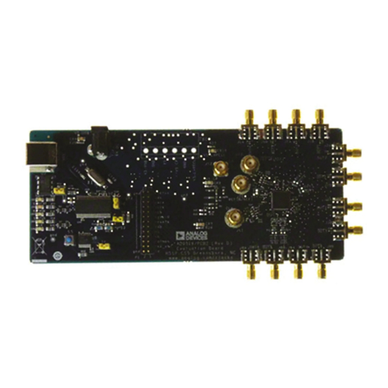
AD9516-x, AD9517-x, and AD9518-x Evaluation Board
FEATURES
Simple power connection using 6 V wall adapter and
on-board LDO voltage regulators
LDOs are easily bypassed for power measurements
8 ac-coupled differential LVPECL SMA connectors
2 ac-coupled LVPECL differential headers
2 dc-coupled differential LVDS SMA connectors that are
reconfigurable to four CMOS SMA connectors
2 dc-coupled LVDS differential headers that are
reconfigurable to four CMOS connectors
SMA connectors for
2 reference inputs
Charge pump output
Clock distribution input
USB connection to PC
Microsoft Windows-based evaluation software with simple
graphical user interface
On-board PLL loop filter
Easy access to digital I/O and diagnostic signals
via I/O header
Status LEDs for diagnostic signals
APPLICATIONS
Clocking of analog-to-digital and digital-to-analog
converters up to 2.9 GHz
Networking and communications line cards
Test and measurement equipment
Wireless base stations, controllers
Clock cleanup/jitter attenuation
Clock distribution
See the last page for an important warning and disclaimers.
AD9516 EVALUATION BOARD
www.BDTIC.com/ADI
Rev. 0 | Page 1 of 16
Evaluation Board User Guide
GENERAL DESCRIPTION
The AD9516-x, AD9517-x, and AD9518-x are very low noise
PLL clock synthesizers featuring an integrated VCO, clock
dividers, and up to 14 outputs. The AD9516 features automatic
holdover and a flexible reference input circuit allowing for very
smooth reference clock switching. The AD9516 family also
features the necessary provisions for an external VCXO.
The AD9516 evaluation board is a compact, easy-to-use
platform for evaluating all features of the AD9516. This user
guide covers all six versions of the AD9516 family, as well as
the AD9517 and AD9518 families (hereafter referred to as
AD951x). The AD9516, AD9517, and AD9518 differ only
in package size, and the number of outputs. The evaluation
software main window for the AD9517 and AD9518 reflects
fewer outputs, but the operation is identical for all devices.
Although the Quick Start Guide to the AD9516 PLL section
applies specifically to the AD9516-3, increasing the N (feed-
back) divider and channel divider increases the VCO frequency
to the allowable frequency range of other AD9516 versions.
For the AD9516-5, which lacks an internal VCO, certain
portions of this document that apply to the internal VCO
(such as VCO calibration) can be ignored.
For convenience, detailed information from the AD9516 data
sheet has been included here. Use this user guide in conjunction
with the AD9516, AD9517, and AD9518 data sheets, as well as
additional documentation available at www.analog.com.
Figure 1.
UG-075
Advertisement
Table of Contents

Related Manuals for Analog Devices AD9516


Summary of Contents for Analog Devices AD9516
-
Page 1: Features
2 dc-coupled LVDS differential headers that are platform for evaluating all features of the AD9516. This user reconfigurable to four CMOS connectors guide covers all six versions of the AD9516 family, as well as SMA connectors for the AD9517 and AD9518 families (hereafter referred to as 2 reference inputs AD951x). -
Page 2: Table Of Contents
Software Installation ..............4 LVDS/CMOS Output Delay Window ........12 Running the Software ..............4 Debug Window ................12 Quick Start Guide to the AD9516 PLL .......... 5 Evaluation Software Menu Items..........13 Evaluation Software Components ..........7 Menu Bar ..................13 Main Window ................ -
Page 3: Evaluation Board Hardware
Evaluation Board User Guide UG-075 EVALUATION BOARD HARDWARE The following instructions are for setting up the physical SIGNAL CONNECTIONS connections to the AD951x evaluation board. To connect signals, use the following steps: When connecting the evaluation board to a PC for the first Connect a signal generator to the J10 SMA connector. -
Page 4: Evaluation Board Software
Quick Start Guide to the AD9516 PLL section for details on the See the Evaluation Board Hardware section for information on individual blocks of the AD951x. -
Page 5: Quick Start Guide To The Ad9516 Pll
PLL. See the AD9516 data sheet and Evaluation Software Components section for a detailed explanation of the various AD9516 features. The following case is an example for the AD9516-3 using the values in Table 1. Table 1. Parameter... - Page 6 UG-075 Evaluation Board User Guide 11. Power down unused drivers, click the numbered triangular Program the R (reference) divider by clicking the R DIVIDER box at the top of the main window. Set symbol on the right side of the main window (see Figure 7), the desired value and click OK (see Figure 12).
-
Page 7: Evaluation Software Components
Evaluation Board User Guide UG-075 EVALUATION SOFTWARE COMPONENTS MAIN WINDOW Figure 8. Evaluation Software Main Window The AD951x evaluation software is composed of subsections When a subwindow closes after clicking OK, the WRITE box that correspond to the major functional blocks of the AD951x. on the main window (under the REGISTER W/R section) may These subsections are listed in the following sections and each blink red. -
Page 8: Pll Reference Input Window
The R divider output is particularly useful. In the example input and PLL output during a reference switchover. Otherwise, used in the Quick Start Guide to the AD9516 PLL section, the the AD951x minimizes the phase disturbance at the output 80 kHz signal is visible on the STATUS pin to ensure that the during a reference switchover. -
Page 9: Register W/R Box
Evaluation Board User Guide UG-075 REGISTER W/R BOX R AND N DELAY WINDOW The REGISTER W/R (write/read) box has four buttons and The AD951x features two delay circuits (one on the reference three check boxes. divider path, and one on the feedback divider path) that allow the user to control the static phase offset between the reference The WRITE button transfers the values stored in the evaluation input and the PLL output. -
Page 10: Phase Frequency Detector (Pfd) Window
UG-075 Evaluation Board User Guide The evaluation software has internal checking to ensure that CHARGE PUMP WINDOW invalid settings are not programmed. For example, the B The Charge Pump Setup window shown in Figure 16 is accessed counter must always be larger than the A counter. Another by clicking the CHARGE PUMP box on the main screen. -
Page 11: Channel Divider Window
Evaluation Board User Guide UG-075 CHANNEL DIVIDER WINDOW LVPECL OUTPUT DRIVER WINDOW The channel divider window shown in Figure 18 is accessed by The LVPECL Output 0 Settings window shown in Figure 20 is clicking the appropriate channel divider. It is usually sufficient accessed by clicking the OUT0 through OUT5 output driver to change only the divide ratio because the evaluation software symbols on the right side of the main window (see Figure 19). -
Page 12: Lvds/Cmos Output Driver Window
UG-075 Evaluation Board User Guide LVDS/CMOS OUTPUT DRIVER WINDOW LVDS/CMOS OUTPUT DELAY WINDOW The LVDS/CMOS Output 6 Settings window shown The Output 6 Delay window shown in Figure 22 is accessed in Figure 21 is accessed by clicking the OUT6 through by clicking the ΔT OUT 6 button on the right of the main OUT9 output driver symbols on the lower right side of screen. -
Page 13: Evaluation Software Menu Items
Evaluation Board User Guide UG-075 EVALUATION SOFTWARE MENU ITEMS Figure 24. Menu Bar MENU BAR Configure Serial Port File Menu The Serial Port Config window allows you to control how the USB controller interacts with the AD951x serial port (see The File menu has the following options: Figure 26). -
Page 14: Ad9516 Pll Loop Filter
It has a transfer function with slight peaking features of the AD9516, including the design of the PLL loop (<3 dB) and loop bandwidths from 75 kHz to 200 kHz. In filter. -
Page 15: Loop Filter For Clock Cleanup
Evaluation Board User Guide UG-075 Table 3. AD9516 Evaluation Board Low Loop Bandwidth LOOP FILTER FOR CLOCK CLEANUP (Clock Cleanup) Filter Component Values The component values in Table 3 are suitable for applications ADIsimCLK Evaluation Board Component where the input reference clock is noisy or for cases where the... -
Page 16: Esd Caution
Information furnished by Analog Devices is believed to be accurate and reliable. However, no responsibility is assumed by Analog Devices for its use, nor for any infringements of patents or other rights of third parties that may result from its use. Analog Devices reserves the right to change devices or specifications at any time without notice.
Need help?
Do you have a question about the AD9516 and is the answer not in the manual?
Questions and answers