Table of Contents
Advertisement
Quick Links
REFCLK
J1
J2
DESCRIPTION
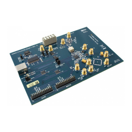
This data sheet describes the AD9956/PCB evaluation board
hardware and software. The current version of software
provides a graphical user interface (GUI) that allows easy
communication with the many on-chip functions of the device.
Rev. 0
Information furnished by Analog Devices is believed to be accurate and reliable.
However, no responsibility is assumed by Analog Devices for its use, nor for any
infringements of patents or other rights of third parties that may result from its use.
Specifications subject to change without notice. No license is granted by implication
or otherwise under any patent or patent rights of Analog Devices. Trademarks and
registered trademarks are the property of their respective owners.
2.7 GHz DDS-Based AgileRF
EVALUATION BOARD FUNCTIONAL BLOCK DIAGRAM
AD9956
RF
DIVIDER
DDS
÷R
SYSCLK
REFCLK
SYSCLK
PLL_OSC
CML DRIVER
PHASE FREQUENCY DETECTOR/
CHARGE PUMP
÷M
PLL_REF
÷N
J3
PLL_OSC
DAC IOUT
DAC IOUT
DRV_OUT
J5
DRV_OUT
50Ω
CP_OUT
VCO AND LOOP FILTER ONLY POPULATED ON
AD9956-VCO/PCB. THESE SOCKETS LEFT VACANT
FOR USER TO POPULATE ON AD9956/PCB
Figure 1.
The AD9956 is a highly sophisticated AgileRF synthesizer with
numerous user-programmable functions. See the AD9956 data
sheet for detailed information about the part.
One Technology Way, P.O. Box 9106, Norwood, MA 02062-9106, U.S.A.
Tel: 781.329.4700
Fax: 781.326.8703
Evaluation Board for
™
Synthesizer
AD9956/PCB
J7
J6
LPF
J4
J16
VCO
LPF
© 2005 Analog Devices, Inc. All rights reserved.
www.analog.com
Advertisement
Table of Contents

Related Manuals for Analog Devices AD9956/PCB


Summary of Contents for Analog Devices AD9956/PCB
- Page 1 Information furnished by Analog Devices is believed to be accurate and reliable. However, no responsibility is assumed by Analog Devices for its use, nor for any infringements of patents or other rights of third parties that may result from its use.
-
Page 2: Table Of Contents
AD9956/PCB TABLE OF CONTENTS Hardware ................... 3 Clock Driver Control, Phase-Frequency Detector & Charge Pump Dialog Box ................7 System Requirements..............3 DUT Signals Dialog Box ..............8 Setup....................3 DUT I/O Dialog Box ..............8 Software ..................... 4 Debug Window................9 Setup....................4 Ordering Information.............. -
Page 3: Hardware
Power Supplies Capability to generate at least 3 inde- or a DSP) pendent dc voltages Analog Devices offers a GUI for the PC; it does not offer Measurement Appropriate measurement device, such as a spectrum analyzer or a high control software for external controllers. -
Page 4: Software
Figure 2. If it fails to detect a working part, a red error message is displayed. Figure 2. AD9956/PCB Evaluation Board Software Status Message upon Successful Load Rev. 0 | Page 4 of 12... -
Page 5: Control Dialog Box
AD9956/PCB CONTROL DIALOG BOX To bypass the RF divider and pipe the REFCLK input directly to the DDS core, select RF Divider RefClk Mux. Even though the Use the Control dialog box to enable and disable individual device functions, program the input clock speed, and toggle... -
Page 6: Profile Dialog Box
AD9956/PCB PROFILE DIALOG BOX Select Clear Frequency Accum. or Clear Phase Accum. to clear and hold the corresponding accumulator. The clear The DDS section of the AD9956 has eight programmable function clears and then holds the contents of the correspond- frequency and phase offset profiles. -
Page 7: Clock Driver Control, Phase-Frequency Detector & Charge Pump Dialog Box
AD9956/PCB CLOCK DRIVER CONTROL, PHASE-FREQUENCY Phase-Frequency Detector/Charge Pump DETECTOR & CHARGE PUMP DIALOG BOX This section controls the PLL components of the AD9956 and the CML (PECL-compliant when properly terminated) clock This dialog box controls the phase detector, charge pump, and driver circuits. -
Page 8: Dut Signals Dialog Box
AD9956/PCB DUT SIGNALS DIALOG BOX DUT I/O DIALOG BOX This dialog box controls the reset, I/O update, and I/O reset This dialog box controls the I/O configuration for the device. signals for the master and slave devices. Click the lock icon... -
Page 9: Debug Window
AD9956/PCB DEBUG WINDOW The Debug Window, shown in Figure 9, lets you directly write to any of the internal registers and subsequently read them back. You can also directly toggle the states of any external inputs such as PS0, PS1, or PS2. -
Page 10: Ordering Information
AD9956/PCB ORDERING INFORMATION ORDERING GUIDE Model Description AD9956/PCB Evaluation Board AD9956-VCO/PCB Evaluation Board with 2.4 GHz VCO and Charge Pump Filter ESD CAUTION ESD (electrostatic discharge) sensitive device. Electrostatic charges as high as 4000 V readily accumulate on the human body and test equipment and can discharge without detection. Although this product features proprietary ESD protection circuitry, permanent damage may occur on devices subjected to high energy electrostatic discharges. - Page 11 AD9956/PCB NOTES Rev. 0 | Page 11 of 12...
- Page 12 AD9956/PCB NOTES © 2005 Analog Devices, Inc. All rights reserved. Trademarks and registered trademarks are the property of their respective owners. EB05278–0–1/05(0) Rev. 0 | Page 12 of 12...
Need help?
Do you have a question about the AD9956/PCB and is the answer not in the manual?
Questions and answers