Sign In
Upload
Manuals
Brands
ST Manuals
Motherboard
STM32 Nucleo-64-P Series
ST STM32 Nucleo-64-P Series Manuals
Manuals and User Guides for ST STM32 Nucleo-64-P Series. We have
3
ST STM32 Nucleo-64-P Series manuals available for free PDF download: User Manual
ST STM32 Nucleo-64-P Series User Manual (52 pages)
Brand:
ST
| Category:
Microcontrollers
| Size: 3 MB
Table of Contents
Figure 1. Nucleo-64-P Board (Top View)
1
Figure 2. Nucleo-64-P Board (Bottom View)
1
Table of Contents
2
Features
7
Ordering Information
8
Codification
8
Table 1. Ordering Information
8
Table 2. Codification Explanation
8
Development Environment
9
System Requirements
9
Development Toolchains
9
Conventions
10
Table 3. ON/OFF Convention
10
Quick Start
11
Getting Started
11
Table 4. Default Jumper Settings
11
Hardware Layout and Configuration
12
Figure 3. Hardware Block Diagram
12
STM32 Nucleo-64-P Board Layout
13
Figure 4. STM32 Nucleo-64-P Board Top Layout
13
Figure 5. STM32 Nucleo-64-P Board Bottom Layout
14
STM32 Nucleo-64-P Board Mechanical Drawing
15
Default Board Configuration
15
Figure 6. STM32 Nucleo-64 -P Board Mechanical Drawing
15
Cuttable PCB
16
Embedded ST-LINK/V2-1
16
Drivers
17
ST-LINK/V2-1 Firmware Upgrade
17
Table 5. ST-LINK Jumper Configuration
17
Figure 7. USB Composite Device
17
Using the ST-LINK/V2-1 to Program/Debug the STM32
18
Using the ST-LINK/V2-1 to Program/Debug an External STM32
18
Application
18
Figure 8. ST-LINK Debugger: Jumper Configuration for On-Board MCU
18
Table 6. Debug Connector SWD
19
Figure 9. ST-LINK Debugger: Jumper Configuration for External MCU
19
Power Supply and Power Selection
20
External Power Supply Input
20
Table 7. Power Supply Capabilities
20
Figure 10. JP5[1-2]: 5V_STL Power Source
21
Figure 11. JP5[3-4]: 5V_VIN Power Source
22
Figure 12. JP5[5-6]: E5V Power Source
23
Table 8. SB9 Configurations
24
Figure 13. JP6[7-8]: 5V_USB_CHG Power Source
24
External Power Supply Output
25
SMPS Power Supply
25
Programming/Debugging When the Power Supply Is Not from
26
ST-LINK (5V_St_Link)
26
OSC Clock Sources
26
LSE: OSC 32 Khz Clock Supply
26
OSC Clock Supply
27
Reset Sources
28
Virtual COM Port: LPUART1/USART1
28
Leds
28
Table 9. LPUART1 Connection
28
Table 10. USART1 Connection
28
Push-Buttons
29
IDD Measurement
29
Jumper Configuration
30
Configuration of the Solder Bridges
30
Table 11. Jumper Settings
30
Table 12. Solder Bridge Configurations and Settings
31
Connectors
35
USB Micro-B Connector CN1
35
Table 13. USB Micro-B Pinout
35
Figure 14. USB Micro-B Connector CN1 (Front View)
35
ARDUINO ® uno V3 Connectors
36
Figure 15. ARDUINO ® Connectors
36
Table 14. ARDUINO ® Connector Pinout
37
Figure 16. ARDUINO ® Connector Pinout
37
ST Morpho Connectors CN5 and CN6
39
Figure 17. ST Morpho Connector
39
External Power Connector
40
Figure 18. ST Morpho Connector Pinout
40
Table 15. External Power Connector Pinout
41
Figure 19. External Power Connector
41
STM32 Nucleo-64-P Board Information
42
Product Marking
42
NUCLEO-L412RB-P Product History
42
Product Identification NUL412RBP$AU1
42
Product Identification NUL412RBP$AU2
42
NUCLEO-L412RB-P Product Limitations
43
Product Identification NUL412RBP$AU1 Limitations
43
Product Identification NUL412RBP$AU2 Limitations
43
NUCLEO-L433RC-P Product History
43
Product Identification NUCLEOL433RCP
43
Product Identification NUL433RCP$AU1
43
NUCLEO-L433RC-P Product Limitations
43
Product Identification NUCLEOL433RCP/ Limitations
43
Product Identification NUL433RCP$AU1 Limitations
43
NUCLEO-L452RE-P Product History
43
Product Identification NUL452REP$AU1
44
NUCLEO-L452RE-P Product Limitations
44
Product Identification NUCLEOL452REP/ Limitations
44
Product Identification NUL452REP$AU1 Limitations
44
Board Revision History
44
MB1319 Revision B-02
44
MB1319 Revision C-01
44
MB1319 Revision C-02
44
Board Known Limitations
44
Board MB1319 Revision B-02 Limitations
44
Assignment
45
Table 16. NUCLEO-L412RB-P, NUCLEO-L433RC-P, and NUCLEO-L452RE-P
45
Federal Communications Commission (FCC)
48
And ISED Canada Compliance
48
FCC Compliance Statement
48
Part 15.19
48
Part 15.21
48
Part 15.105
48
ISED Canada Compliance Statement
48
Compliance Statement
49
Déclaration de Conformité
49
Ce / Red
50
En55032 / Cispr32
50
Revision History
51
Table 17. Document Revision History
51
Advertisement
ST STM32 Nucleo-64-P Series User Manual (55 pages)
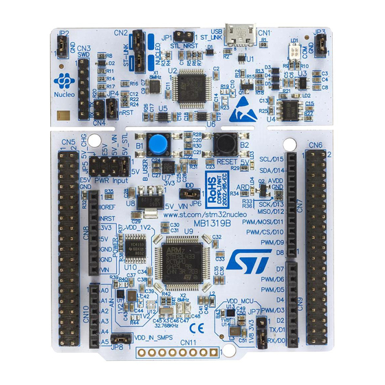
STM32 Nucleo-64-P boards
Brand:
ST
| Category:
Motherboard
| Size: 1 MB
Table of Contents
Figure 1. Nucleo-64-P Board (Top View)
1
Figure 2. Nucleo-64-P Board (Bottom View)
1
Table of Contents
2
1 Features
6
2 Product Marking
6
3 Ordering Information
7
4 Conventions
7
Table 1. Ordering Information
7
Table 2. Codification Explanation
7
Table 3. ON/OFF Convention
7
5 System Requirements
8
6 Development Toolchains
8
7 Demonstration Software
8
8 Quick Start
9
Getting Started
9
9 Hardware Layout and Configuration
10
Figure 3. Hardware Block Diagram
10
STM32 Nucleo-64-P Board Layout
11
Figure 4. STM32 Nucleo-64-P Board Top Layout
11
Figure 5. STM32 Nucleo-64-P Board Bottom Layout
12
STM32 Nucleo-64-P Board Mechanical Drawing
13
Default Board Configuration
13
Figure 6. STM32 Nucleo-64 -P Board Mechanical Drawing
13
Cuttable PCB
14
Embedded ST-LINK/V2-1
14
Table 4. Default Jumper Settings
14
Drivers
15
Figure 7. USB Composite Device
15
ST-LINK/V2-1 Firmware Upgrade
15
Table 5. ST-LINK Jumper Configuration
15
Application
16
Figure 8. ST-LINK Debugger: Jumper Configuration for On-Board MCU
16
Using the ST-LINK/V2-1 to Program/Debug an External STM32
16
Using the ST-LINK/V2-1 to Program/Debug the STM32
16
Figure 9. ST-LINK Debugger: Jumper Configuration for External MCU
17
Table 6. Debug Connector SWD
17
Power Supply and Power Selection
18
External Power Supply Input
18
Table 7. Power Supply Capabilities
18
Figure 10. JP5[1-2]: 5V_STL Power Source
19
Figure 11. JP5[3-4]: 5V_VIN Power Source
20
Figure 12. JP5[5-6]: E5V Power Source
21
Table 8. SB9 Configurations
22
Figure 13. JP6[7-8]: 5V_USB_CHG Power Source
22
External Power Supply Output
23
SMPS Power Supply
23
Programming/Debugging When the Power Supply Is Not from
24
ST-LINK (5V_St_Link)
24
OSC Clock Sources
24
LSE: OSC 32 Khz Clock Supply
24
OSC Clock Supply
25
Reset Sources
26
Virtual COM Port: LPUART1/USART1
26
Leds
26
Table 9. LPUART1 Connection
26
Table 10. USART1 Connection
26
Push Buttons
27
IDD Measurement
27
Jumper Configuration
28
Configuration of the Solder Bridges
28
Table 11. Jumper Settings
28
Table 12. Solder Bridge Configurations and Settings
29
Connectors
33
Figure 14. USB Micro-B Connector CN1 (Front View)
33
Table 13. USB Micro-B Pinout
33
USB Micro-B Connector CN1
33
Arduino uno V3 Connectors
34
Figure 15. Arduino Connectors
34
Figure 16. Arduino Connector Pinout
35
Table 14. Arduino Connector Pinout
35
Figure 17. ST Morpho Connector
37
ST Morpho Connectors CN5 and CN6
37
External Power Connector
38
Figure 18. ST Morpho Connector Pinout
38
Figure 19. External Power Connector
39
I/O Assignment
40
Table 16. NUCLEO-L412RB-P, NUCLEO-L433RC-P and NUCLEO-L452RE-P
40
Appendix A NUCLEO-L412RB-P, NUCLEO-L433RC-P and NUCLEO-L452RE-P
43
Table 15. External Power Connector Pinout
39
Appendix B Electrical Schematics
43
Figure 20. Top and Power
44
Figure 21. STM32 I/Os
45
Figure 22. STM32 Power
46
Figure 23. Arduino Extension Connectors
47
Figure 24. Main Power 5 V, 3.3 V
48
Figure 25. STM32 Power SMPS
49
Figure 26. ST-LINK/V2-1
50
Appendix C Federal Communications Commission (FCC)
51
And Industry Canada (IC) Compliance
51
FCC Compliance Statement
51
Part 15.19
51
Part 15.105
51
Part 15.21
51
IC Compliance Statement
51
Compliance Statement
52
Déclaration de Conformité
52
Appendix D CISPR32
53
Warning
53
Revision History
54
Table 17. Document Revision History
54
ST STM32 Nucleo-64-P Series User Manual (55 pages)
Brand:
ST
| Category:
Motherboard
| Size: 1 MB
Table of Contents
Figure 1. Nucleo-64-P Board (Top View)
1
Figure 2. Nucleo-64-P Board (Bottom View)
1
Table of Contents
2
1 Features
6
2 Product Marking
6
3 Ordering Information
7
4 Conventions
7
Table 1. Ordering Information
7
Table 2. Codification Explanation
7
Table 3. ON/OFF Convention
7
5 System Requirements
8
6 Development Toolchains
8
7 Demonstration Software
8
8 Quick Start
9
Getting Started
9
9 Hardware Layout and Configuration
10
Figure 3. Hardware Block Diagram
10
STM32 Nucleo-64-P Board Layout
11
Figure 4. STM32 Nucleo-64-P Board Top Layout
11
Figure 5. STM32 Nucleo-64-P Board Bottom Layout
12
STM32 Nucleo-64-P Board Mechanical Drawing
13
Default Board Configuration
13
Figure 6. STM32 Nucleo-64 -P Board Mechanical Drawing
13
Cuttable PCB
14
Embedded ST-LINK/V2-1
14
Table 4. Default Jumper Settings
14
Drivers
15
Figure 7. USB Composite Device
15
ST-LINK/V2-1 Firmware Upgrade
15
Table 5. ST-LINK Jumper Configuration
15
Figure 8. ST-LINK Debugger: Jumper Configuration for On-Board MCU
16
Using the ST-LINK/V2-1 to Program/Debug an External STM32 Application
16
Using the ST-LINK/V2-1 to Program/Debug the STM32
16
Figure 9. ST-LINK Debugger: Jumper Configuration for External MCU
17
Table 6. Debug Connector SWD
17
Power Supply and Power Selection
18
External Power Supply Input
18
Table 7. Power Supply Capabilities
18
Figure 10. JP5[1-2]: 5V_STL Power Source
19
Figure 11. JP5[3-4]: 5V_VIN Power Source
20
Figure 12. JP5[5-6]: E5V Power Source
21
Table 8. SB9 Configurations
22
Figure 13. JP6[7-8]: 5V_USB_CHG Power Source
22
External Power Supply Output
23
SMPS Power Supply
23
Programming/Debugging When the Power Supply Is Not from ST-LINK (5V_St_Link)
24
OSC Clock Sources
24
LSE: OSC 32 Khz Clock Supply
24
OSC Clock Supply
25
Reset Sources
26
Virtual COM Port: LPUART1/USART1
26
Leds
26
Table 9. LPUART1 Connection
26
Table 10. USART1 Connection
26
Push Buttons
27
IDD Measurement
27
Jumper Configuration
28
Configuration of the Solder Bridges
28
Table 11. Jumper Settings
28
Table 12. Solder Bridge Configurations and Settings
29
Connectors
33
Figure 14. USB Micro-B Connector CN1 (Front View)
33
Table 13. USB Micro-B Pinout
33
USB Micro-B Connector CN1
33
Arduino uno V3 Connectors
34
Figure 15. Arduino Connectors
34
Figure 16. Arduino Connector Pinout
35
Table 14. Arduino Connector Pinout
35
Figure 17. ST Morpho Connector
37
ST Morpho Connectors CN5 and CN6
37
External Power Connector
38
Figure 18. ST Morpho Connector Pinout
38
Figure 19. External Power Connector
39
I/O Assignment
40
Table 16. NUCLEO-L412RB-P, NUCLEO-L433RC-P and NUCLEO-L452RE-P
40
Appendix A NUCLEO-L412RB-P, NUCLEO-L433RC-P and NUCLEO-L452RE-P
43
Table 15. External Power Connector Pinout
39
Appendix B Electrical Schematics
43
Figure 20. Top and Power
44
Figure 21. STM32 I/Os
45
Figure 22. STM32 Power
46
Figure 23. Arduino Extension Connectors
47
Figure 24. Main Power 5 V, 3.3 V
48
Figure 25. STM32 Power SMPS
49
Figure 26. ST-LINK/V2-1
50
Appendix C Federal Communications Commission (FCC)
51
And Industry Canada (IC) Compliance
51
FCC Compliance Statement
51
Part 15.19
51
Part 15.105
51
Part 15.21
51
IC Compliance Statement
51
Compliance Statement
52
Déclaration de Conformité
52
Appendix D CISPR32
53
Warning
53
Revision History
54
Table 17. Document Revision History
54
Advertisement
Advertisement
Related Products
ST STM32 Nucleo-144 board
ST STM32 Nucleo-32
ST STM32 Nucleo-64
ST STM32 NUCLEO-F042K6
ST STM32 NUCLEO-F303K8
ST STM32 NUCLEO-L031K6
ST STM32 NUCLEO-F030R8
ST STM32 NUCLEO-F070RB
ST STM32 NUCLEO-F072RB
ST STM32 NUCLEO-F091RC
ST Categories
Motherboard
Computer Hardware
Microcontrollers
Control Unit
Controller
More ST Manuals
Login
Sign In
OR
Sign in with Facebook
Sign in with Google
Upload manual
Upload from disk
Upload from URL