Table of Contents
Advertisement
Introduction
The STM32 Nucleo-64-P boards (NUCLEO-L412RB-P, NUCLEO-L433RC-P and
NUCLEO-L452RE-P) provide an affordable and flexible way for users to try out new
concepts and build prototypes with the STM32 microcontroller and the external SMPS
(switched mode power supply), which provides various combinations of performance, power
consumption and features.
™
Arduino
expanding the functionality of the Nucleo open development platform with a wide choice of
specialized shields.
The STM32 Nucleo-64-P boards do not require any separate probe, as they integrate the
ST-LINK/V2-1 debugger/programmer. The STM32 Nucleo-64-P boards come with the
comprehensive free STM32 software libraries and examples that are available with the
STM32Cube package.
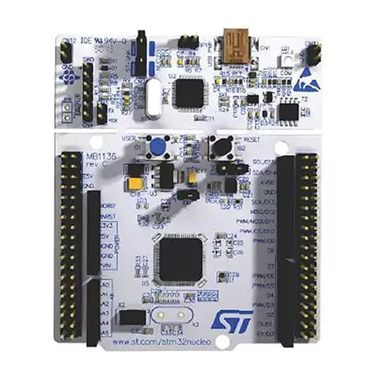
Figure 1. Nucleo-64-P board (top view)
Pictures are not contractual.
August 2018
Uno V3 connectivity and ST morpho headers provide an easy means of
STM32 Nucleo-64-P boards
Figure 2. Nucleo-64-P board (bottom view)
UM2206 Rev 3
UM2206
User manual
www.st.com
1/55
1
Advertisement
Table of Contents

Subscribe to Our Youtube Channel
Related Manuals for ST NUCLEO-L433RC-P


Summary of Contents for ST NUCLEO-L433RC-P
-
Page 1: Figure 1. Nucleo-64-P Board (Top View)
™ Arduino Uno V3 connectivity and ST morpho headers provide an easy means of expanding the functionality of the Nucleo open development platform with a wide choice of specialized shields. The STM32 Nucleo-64-P boards do not require any separate probe, as they integrate the ST-LINK/V2-1 debugger/programmer. -
Page 2: Table Of Contents
Embedded ST-LINK/V2-1 ........14... - Page 3 Arduino Uno V3 connectors ........34 10.3 ST morpho connectors CN5 and CN6 ......37 10.4 External power connector .
- Page 4 ST-LINK jumper configuration ........
- Page 5 ST-LINK debugger: jumper configuration for on-board MCU ..... . . 16 Figure 9. ST-LINK debugger: jumper configuration for external MCU ......17 Figure 10.
-
Page 6: Features
Any consequences deriving from such usage will not be at ST charge. In no event, ST will be liable for any customer usage of these engineering sample tools as reference design or in production. -
Page 7: Ordering Information
To order the Nucleo-64-P board corresponding to the targeted STM32, refer to Table Table 1. Ordering information Order code Target STM32 NUCLEO-L412RB-P STM32L412RBT6P NUCLEO-L433RC-P STM32L433RCT6P NUCLEO-L452RE-P STM32L452RET6P The meaning of the codification is explained in Table Table 2. Codification explanation... -
Page 8: System Requirements
The demonstration software, included in the STM32Cube MCU Package, is preloaded in the STM32 Flash memory for easy demonstration of the device peripherals in standalone mode. The latest versions of the demonstration source code and associated documentation can be downloaded from the www.st.com/stm32nucleo webpage. ® a. macOS is a trademark of Apple Inc.\nregistered in the U.S. -
Page 9: Quick Start
For a correct identification of all device interfaces from the host PC, install the Nucleo USB driver available on the www.st.com/ stm32nucleo webpage, prior connecting the board. To power the board connect the Nucleo-64-P board to a PC with a USB cable ‘type A to micro-B’... -
Page 10: Hardware Layout And Configuration
The STM32 Nucleo-64-P board is designed around the STM32 microcontrollers in a 64-pins LQFP package. Figure 3 illustrates the connection between the STM32 and the peripherals (ST-LINK/V2-1, push-buttons, LEDs, Arduino Uno V3 connector and ST morpho connectors). Figure 4 Figure 5 show the location of these features on the STM32 Nucleo-64-P board. -
Page 11: Stm32 Nucleo-64-P Board Layout
UM2206 Hardware layout and configuration STM32 Nucleo-64-P board layout Figure 4. STM32 Nucleo-64-P board top layout ST-LINK RST: JP1 USB_STLINK: CN1 ST-LINK debugger: COM LED: LD1 SWD: CN3 STLINK_3V3: U3 nRST: JP4 ST-LINK STM32: U2 UART VPN: CN4 STLINK_5V_SW: U4... -
Page 12: Figure 5. Stm32 Nucleo-64-P Board Bottom Layout
Hardware layout and configuration UM2206 Figure 5. STM32 Nucleo-64-P board bottom layout 12/55 UM2206 Rev 3... -
Page 13: Stm32 Nucleo-64-P Board Mechanical Drawing
UM2206 Hardware layout and configuration STM32 Nucleo-64-P board mechanical drawing Figure 6. STM32 Nucleo-64 -P board mechanical drawing 9.2.1 Default board configuration By default the STM32 Nucleo-64-P board is delivered with the external SMPS 1.1 V enabled and V @3.3 V. It is possible to set the board for V @1.8 V. -
Page 14: Cuttable Pcb
An STM32 Nucleo-64-P board is divided into two parts: ST-LINK and target STM32. The ST-LINK part of the PCB can be cut out to reduce the board size. In this case the remaining target STM32 part can only be powered by V , E5V and 3.3 V on the ST morpho connector... -
Page 15: Drivers
ST-LINK/V2-1 firmware upgrade The ST-LINK/V2-1 embeds a firmware upgrade mechanism for in-situ upgrade through the USB port. As the firmware may evolve during the lifetime of the ST-LINK/V2-1 product (for example new functionalities, bug fixes, support for new microcontroller families), it is recommended to keep the ST-LINK/V2-1 firmware up to date before starting to use an STM32 Nucleo-64-P board. -
Page 16: Using The St-Link/V2-1 To Program/Debug The Stm32
9.4.4 Using the ST-LINK/V2-1 to program/debug an external STM32 application. It is very easy to use the ST-LINK/V2-1 to program the STM32 on an external application. Simply remove the two jumpers from CN2, as shown in Figure 9, and connect the... -
Page 17: Table 6. Debug Connector Swd
UM2206 Hardware layout and configuration Figure 9. ST-LINK debugger: jumper configuration for external MCU ST-LINK jumper OFF: CN2 [1-2] and [3-4] SWD connector: CN3 Table 6. Debug connector SWD Connector Pin name Signal name STM32 pin Function number VDD_TARGET: from application... -
Page 18: Power Supply And Power Selection
5V_ST_LINK is a DC power with limitation from ST-LINK USB connector (USB type Micro-B connector of ST-LINK/V2-1). In this case JP5 jumper should be on pins 1 and 2 to select 5V_STL power source on silkscreen of JP5. This is the default setting. If the USB enumeration succeeds, the 5V_ST_LINK power is enabled, by asserting the PWR_ENn signal (from STM32F103CBT6). -
Page 19: Figure 10. Jp5[1-2]: 5V_Stl Power Source
PWR connector: JP5 [1-2] ON VIN (5V_VIN) is the 7-12 V DC power from Arduino CN8 pin 8 named V on Arduino connector silkscreen or from ST morpho connector CN5 pin 24. In this case JP5 jumper UM2206 Rev 3 19/55... -
Page 20: Figure 11. Jp5[3-4]: 5V_Vin Power Source
CN8 pin 8 CN5 pin 24 E5V is the DC power coming from external (5V DC power from ST morpho connector CN5 pin 6). In this case JP5 jumper should be on pins 5 and 6 to select E5V power source on silkscreen of JP5. -
Page 21: Figure 12. Jp5[5-6]: E5V Power Source
JP5 [5-6] ON E5V: CN5 pin 6 5V_USB_CHARGER is the DC power charger connected to USB ST-LINK (CN1). To select the 5V_USB_CHARGER power source on silkscreen of JP5, the jumper of JP5 should be on pins 7 and 8. In this case, if the STM32 Nucleo-64-P board is powered by an external USB charger the debug is not available. -
Page 22: Table 8. Sb9 Configurations
Solder bridge SB9 can be used to bypass the USB power protection ST890. (This is not an ST recommended setting). SB9 can be set in case the board is powered by the USB of the PC and maximum current consumption on 5V_STLINK does not exceed 100 mA (including extension board or Arduino shield power consumption). -
Page 23: External Power Supply Output
1.8 V: JP7 to pins 2 and 3 (best ULPBench score) Note: The ST-LINK is still available in this configuration thanks to the level shifters U5 and U6. For all general information concerning design recommendations for the STM32 with external SMPS, refer to the Design recommendations for STM32L4xxxx with external... -
Page 24: Programming/Debugging When The Power Supply Is Not From
LSE which is the 32.768 KHz crystal for the STM32 embedded RTC • MCO which is the 8 MHz clock from the ST-LINK MCU for the STM32 microcontroller • HSE which is the 8 MHz oscillator for the STM32 microcontroller. This clock is not implemented on the STM32 Nucleo-64-P board. -
Page 25: Osc Clock Supply
There are four ways to configure the pins corresponding to the external-high-speed clock (HSE): MCO from ST-LINK (Default: not connected): MCO output of ST-LINK MCU is used as an input clock. This frequency cannot be changed, it is fixed at 8 MHz and connected to PH0 OSC_IN of the STM32 microcontroller. -
Page 26: Reset Sources
LPUART1 to support the virtual COM port • Communication between target STM32 and Arduino and ST morpho connector is enabled on USART1 The virtual COM port settings are configured as: 115200 b/s, 8 bits data, no parity, 1 stop bit, no flow control. -
Page 27: Push Buttons
Hardware layout and configuration LD1 COM: LD1 is a bi-color LED. LD1 default status is red. LD1 turns to green to indicate that communication is in progress between the PC and the ST-LINK/V2-1 as follow: • Slow blinking red/off: at power-on before USB initialization •... -
Page 28: Jumper Configuration
Used to reset ST-LINK MCU STLK_RST Normal use JP2/JP3 GND probe ST-LINK able to reset STM32 T_NRST ST-LINK not able to reset STM32 ON [1-2] 5 V from ST-LINK ON [3-4] 5 V from V 7-12 V 5 V Power selection... -
Page 29: Table 12. Solder Bridge Configurations And Settings
SWO not connected through level shifter SWO level SB10 SWO connected through level shifter to target MCU shifter by-pass for 1.8 V I/O configuration SWO_MCU connected between ST-LINK and target STM32 SWO_MCU SB11 SWO_MCU not connected between ST-LINK and target STM32... - Page 30 DD_1V2 SB30 / SB46 powered directly by U11/U12. Switch U10 DD_1V2 is not used (not recommended, see AN4978 on the U11/U12 www.st.com website) SMPS out powered directly by U11/U12. Switch U10 1.1 V DD_1V2 is not used. (not recommended, see AN4978 on the www.st.com...
- Page 31 HSE provided by External HSE CLK X2 SB67/SB69 HSE NOT provided by External HSE CLK X2 HSE CLK PH1 connected to ST morpho connector I/O usage selection SB68 PH1 NOT connected to ST morpho connector PH0 connected to ST morpho connector...
- Page 32 Hardware layout and configuration UM2206 Table 12. Solder bridge configurations and settings (continued) Definition Bridge State Comment SB84 ADP5301 EN pin driven by I/O: SMPS_EN PA4 ADP5301 U9 SB84 / SB85 EN selection SB85 ADP5301 always enabled (level 1) SB86 ADP5301 set in PWM mode (500 mA out, low efficiency) ADP5301...
-
Page 33: Connectors
CN11: External SMPS connector 10.1 USB Micro-B connector CN1 The USB connector CN1 is used to connect the embedded ST-LINK/V2-1 to the PC for programming and debugging the STM32 Nucleo-64-P board microcontroller. Figure 14. USB Micro-B connector CN1 (front view) -
Page 34: Arduino Uno V3 Connectors
Connectors UM2206 10.2 Arduino Uno V3 connectors The Arduino connectors CN7, CN8 CN9 and CN10 (see Figure 15) are female connectors compatible with Arduino standard. Most shields designed for Arduino can fit to the STM32 Nucleo-64-P board. The Arduino connectors on STM32 Nucleo-64-P board support the Arduino Uno V3. Figure 15. -
Page 35: Table 14. Arduino Connector Pinout
UM2206 Connectors Figure 16. Arduino connector pinout NUCLEO_L4xxRx-P PC10 PC11 PC12 AVDD AVDD BOOT0 5V-STLINK PB13 IOREF PA10 IOREF PB14 PB12 NRST NRST PB15 PA13 PB11 PA11 PA14 PC13 PC14 PB10 PC15 PA15 AGND VBAT PA12 PA2/PA9 PA3/PA10 CN10 Arduino orpho Note: Arduino Uno V3 D0 and D1 signals are connected by default on USART1 (MCU I/O PA9... - Page 36 Connectors UM2206 Table 14. Arduino connector pinout (continued) Connector Pin number Pin name Signal name STM32 pin Function ADC1_IN5 ADC1_IN6 ADC1_IN4 ADC1_IN3 CN10 ADC1_IN2/I2C3_ ADC1_IN1/I2C3_ SCL/D15 ARD_D15 I2C1_SCL SDA/D14 ARD_D14 I2C1_SDA AVDD VREF VREF Ground SCK/D13 ARD_D13 PB13 SPI2_SCK MISO/D12 ARD_D12 PB14 SPI2_MISO...
-
Page 37: St Morpho Connectors Cn5 And Cn6
UM2206 Connectors 10.3 ST morpho connectors CN5 and CN6 The ST morpho connectors CN5 and CN6 are male pin headers accessible on both sides of the STM32 Nucleo-64-P board (see Figure 17). All signals and power pins, except 1.2 V of the STM32, are available on the ST morpho connectors. These DD_CORE connectors can also be probed by an oscilloscope, logical analyzer or voltmeter. -
Page 38: External Power Connector
Connectors UM2206 Figure 18. ST morpho connector pinout NUCLEO_L4xxRx-P PC10 PC11 PC12 AVDD AVDD BOOT0 5V-STLINK PB13 IOREF IOREF PA10 PB14 PB12 NRST NRST PB15 PA13 PB11 PA11 PA14 PC13 PC14 PB10 PC15 PA15 AGND VBAT PA12 PA2/PA9 PA3/PA10 CN10... -
Page 39: Table 15. External Power Connector Pinout
UM2206 Connectors Figure 19. External power connector The related pinout for external power connector is listed in Table Table 15. External power connector pinout Connector Signal name STM32 pin Function number @ 3.3 V supply MCU Core PWR 1.2 V/1.1 V OUTCORE DD_1V2 : 1.8 V / 3.3 V... -
Page 40: I/O Assignment
NUCLEO-L412RB-P, NUCLEO-L433RC-P and NUCLEO-L452RE-P I/O assignment UM2206 Appendix A NUCLEO-L412RB-P, NUCLEO-L433RC-P and NUCLEO-L452RE-P I/O assignment Table 16. NUCLEO-L412RB-P, NUCLEO-L433RC-P and NUCLEO-L452RE-P I/O assignment Pin name Signal or label Main feature / optional feature (SB) PWR V PC13 PC13 User Button / I/O... - Page 41 UM2206 NUCLEO-L412RB-P, NUCLEO-L433RC-P and NUCLEO-L452RE-P I/O assignment Table 16. NUCLEO-L412RB-P, NUCLEO-L433RC-P and NUCLEO-L452RE-P I/O assignment (continued) Pin name Signal or label Main feature / optional feature (SB) PWR GND PWR V 1.8 V / 3.3 V DD_MCU DD_MCU PB12 PB12...
- Page 42 NUCLEO-L412RB-P, NUCLEO-L433RC-P and NUCLEO-L452RE-P I/O assignment UM2206 Table 16. NUCLEO-L412RB-P, NUCLEO-L433RC-P and NUCLEO-L452RE-P I/O assignment (continued) Pin name Signal or label Main feature / optional feature (SB) PWR GND PWR V 1.8 V / 3.3 V DD_MCU DD_MCU 42/55 UM2206 Rev 3...
-
Page 43: Appendix B Electrical Schematics
– STM32 I/Os (see Figure – STM32 Power (see Figure – Arduino extension connectors (see Figure – Main Power 5 V and 3.3 V (see Figure – STM32 power SMPS (see Figure – ST-LINK/V2-1 (see Figure UM2206 Rev 3 43/55... -
Page 44: Figure 20. Top And Power
BLISTER MB1319C NUCLEO64_BLISTER HW104 HW105 HW106 HW107 HW108 HW109 Title: mb1319 Top: hierarchical view Project: NUCLEO64 ext-SMPS Variant: L412RB_P Revision: C 01 Reference: MB1319 LOGO NUCLEO LOGO ST LOGO CE LOGO ESD LOGO ROHS LOGO STM32 Size: Date: 05-January-2018 Sheet:... -
Page 45: Figure 21. Stm32 I/Os
Figure 21. STM32 I/Os PA[0..15] PB[0..15] PC[0..15] PH[0..1] For IC compatible config 1: PA[0..15] PB[0..15] PC[0..15] PH[0..1] USER BUTTON Pin25: PB0: SB63 Pin26: PB1: SB52 Pin27: PB2: SB44 VDD_MCU MCU_IOs SB59 Pin54: PB3: SB18 SB63 Pin55: PB4: SB22 HW17 STLINK_TX SB66 SB57 Pin56: PB5: SB26... -
Page 46: Figure 22. Stm32 Power
Figure 22. STM32 Power MCU PWR SUPPLIES AVDD SB74 use to bypass L2 when Nucleo powered by Arduino AVDD SB74 SB78 MCU_PWR VDD_MCU SB77 VDDA/VREF+ VSSA/VREF- 600R@100MHz VBAT SB61 VDD_MCU VBAT SB65 AGND VDD_4 VSS_4 VDD_1 VSS_1 VDD_MCU VDD_3 VSS_3 SB25 SB24 VDDUSB... -
Page 47: Figure 23. Arduino Extension Connectors
Figure 23. Arduino extension connectors SB21 SB15 SB14 IOREF SELECTION IOREF= 3V3 Closed Open Open IOREF = 3V3_PER Open Closed Open IOREF = VDD_MCU Open Open Closed Default Mainly for 1V8 compatibility 3V3_PER PA[0..15] PA[0..15] 510R PB[0..15] SB21 GREEN PB[0..15] IOREF SB15 3V3_PER... -
Page 48: Figure 24. Main Power 5 V, 3.3 V
VIN / 5V PWR LD1117S50TR 5V_VIN Vout Gnd Tab 10uF 10uF 5V PWR SELECTION 5V_STLINK_SW 5V_VIN 5V_USB_CHG 510R Jumper_Header_4x2 E5V from ST-Morpho connector 5V_USB_CHG from USB-STLINK CONNECTOR GREEN 3V3 PWR JP6 for IDD Measurement LD39050PU33R SB13 VOUT 100nF 100nF 3V3_PER SB20 Title:... -
Page 49: Figure 25. Stm32 Power Smps
Figure 25. STM32 power SMPS VDD_MCU_SELECTION Default: JP7[1-2] JP7[1-2]: NO SMPS SELECTION, VDD = VDD_MCU VDD_MCU U13 AND U14 ARE EXCLUSIVELY POPULATED ST1PS01EJR Header 3x1 SB87 VDD_MCU table SB76 VDD_SMPS_1V8 VDD_MCU= VDD [1-2] Open SB76: DEFAULT: OPEN Closed: when VDD_MCU is provided from U13 or U14 2.2uH 2.6A 0.100R JP7[3-2]: SMPS SELECTION, VDD_MCU = 1V8 VDD_MCU = 1V8... -
Page 50: Figure 26. St-Link/V2-1
VDDA PB15 AIN_1 T_JTMS 3V3_PER PB14 T_JTCK Header 4x1 Jumpers ON --> NUCLEO Selected PB13 PB12 Jumpers OFF --> ST-LINK Selected 100R HW10 T_SWDIO_IN STLK_TX STLINK_RX STLK_RX 3V3_ST_LINK Header 2x1 UART_TX LEVEL SHIFTER for MCU_1V8 SW LEVEL SHIFTER FOR MCU_1V8... -
Page 51: Appendix C Federal Communications Commission (Fcc)
UM2206 Federal Communications Commission (FCC) and Industry Canada (IC) Compliance Appendix C Federal Communications Commission (FCC) and Industry Canada (IC) Compliance FCC Compliance Statement C.1.1 Part 15.19 This device complies with Part 15 of the FCC Rules. Operation is subject to the following two conditions: (1) this device may not cause harmful interference, and (2) this device must accept any interference received, including interference that may cause undesired operation. -
Page 52: Compliance Statement
Federal Communications Commission (FCC) and Industry Canada (IC) Compliance UM2206 C.2.1 Compliance Statement Notice: This device complies with Industry Canada licence-exempt RSS standard(s). Operation is subject to the following two conditions: (1) this device may not cause interference, and (2) this device must accept any interference, including interference that may cause undesired operation of the device. -
Page 53: Appendix D Cispr32
UM2206 CISPR32 Appendix D CISPR32 Warning Warning: This device is compliant with Class B of CISPR32. In a residential environment, this equipment may cause radio interference. Avertissement: Cet équipement est conforme à la Classe B de la CISPR 32. Dans un environnement résidentiel, cet équipement peut créer des interférences radio. -
Page 54: Revision History
Extended document scope to the NUCLEO-L412RB-P board: updated Introduction Table 1: Ordering information,ST1PS02 voltage selection in Table 12: Solder bridge configurations and settings, and Table 16: NUCLEO-L412RB-P, NUCLEO-L433RC-P and 23-Aug-2018 NUCLEO-L452RE-P I/O assignment. Updated Chapter 2: Product marking. Updated schematics from Figure 20 Figure 26 board revision C-01. - Page 55 ST products and/or to this document at any time without notice. Purchasers should obtain the latest relevant information on ST products before placing orders. ST products are sold pursuant to ST’s terms and conditions of sale in place at the time of order acknowledgement.
Need help?
Do you have a question about the NUCLEO-L433RC-P and is the answer not in the manual?
Questions and answers