Table of Contents
Advertisement
Quick Links
UM1667
User manual
STM32429I-EVAL evaluation board for STM32F429 MCUs
Introduction
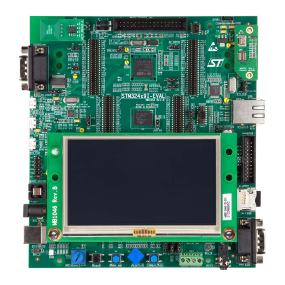
The STM32429I-EVAL evaluation board is a complete demonstration and development
®
®
platform for STMicroelectronics Arm
Cortex
-M4 core-based STM32F429NIH6
2
2
microcontrollers. It features three I
C, six SPI with two muxed full-duplex I
S, SDIO, four
USART, four UART, two CAN, three 12-bit ADC, two 12-bit DAC, one SAI, 8- to 14-bit digital
camera module interface, internal 256+4 Kbyte SRAM and 2-Mbyte Flash memory, USB HS
OTG and USB FS OTG, Ethernet MAC, FMC interface, JTAG debugging support. This
evaluation board can be used as a reference design for user application development but it
is not considered as a final application.
The full range of hardware features on the board helps the user to evaluate all peripherals
(such as USB OTG HS, USB OTG FS, Ethernet, motor control, CAN, microSD™ card,
USART, Audio DAC and ADC, digital microphone, IrDA, CAN, RF-EEPROM, SRAM, NOR
Flash memory, SDRAM, 4.3" TFT LCD with a resistive touch panel, and others) and develop
his own applications. Extension headers make it possible to easily connect a daughterboard
for specific applications development.
The integrated ST-LINK/V2 provides an embedded in-circuit debugger and programmer for
the STM32 MCU.
Figure 1. STM32429I-EVAL evaluation board
Picture is not contractual.
May 2021
UM1667 Rev 3
1/59
www.st.com
1
Arrow.com.
Downloaded from
Advertisement
Table of Contents

Related Manuals for ST STM32429I-EVAL1


Summary of Contents for ST STM32429I-EVAL1
- Page 1 Flash memory, SDRAM, 4.3" TFT LCD with a resistive touch panel, and others) and develop his own applications. Extension headers make it possible to easily connect a daughterboard for specific applications development. The integrated ST-LINK/V2 provides an embedded in-circuit debugger and programmer for the STM32 MCU. Figure 1. STM32429I-EVAL evaluation board Picture is not contractual.
-
Page 2: Table Of Contents
Contents UM1667 Contents Features ........... 7 Ordering information . - Page 3 TFT LCD connector CN20 ........42 5.19 ST-LINK/V2 USB Type B connector CN21 ......43 5.20 CAN D-type 9-pin male connector CN22 .
- Page 4 Contents UM1667 6.3.4 MB1020 ..........46 Board known limitations .
- Page 5 UM1667 List of tables List of tables Table 1. Ordering information ............8 Table 2.
- Page 6 List of figures UM1667 List of figures Figure 1. STM32429I-EVAL evaluation board ......... . . 1 Figure 2.
-
Page 7: Features
Extension connectors and memory connectors for daughterboard or wrapping board • Six 5 V power supply options: power jack, ST-LINK/V2, User USB HS, User USB FS1, User USB FS2, daughterboard • Debug with JTAG/SWD, ETM trace, and on-board ST-LINK/V2 debugger/programmer •... -
Page 8: Ordering Information
Ordering information UM1667 Ordering information To order the STM32429I-EVAL evaluation board, refer to Table 1. Additional information is available from the datasheet and reference manual of the target STM32. Table 1. Ordering information Order code Board reference Target STM32 MB1045 MB1046 STM32429I-EVAL STM32F429NIH6... -
Page 9: Development Environment
For more information and to download the latest version, refer to the STM32429I-EVAL demonstration software on www.st.com. Delivery recommendations Some verifications are needed before using the board for the first time to make sure that nothing was damaged during shipment and that no components are unplugged or lost. -
Page 10: Hardware Layout And Configuration
STM32F429NIH6 and peripherals (SDRAM, SRAM, NOR Flash memory, camera module, color LCD, USB OTG connectors, motor control connector, USART, IrDA, Ethernet, audio, CAN, RF-EEPROM, microSD™ card and embedded ST-LINK). Figure 3 helps the user to locate these features on the actual evaluation board. -
Page 11: Figure 3. Evaluation Board Layout
RJ45 connector OTG2 HS CN14 OTG1 FS CN16 CN15 JTAG/SWD OTG2 FS CN17 MicroSD card CN18 power jack CN21 ST-LINK/V2 CN22 LD11 ST-LINK/V2 COM LED CN20 CN23 digital color LCD audio jack microphone 4 color connector LEDS (Left) digital... -
Page 12: Development And Debug Support
UM1667 Development and debug support Version 2 of the ST-LINK (ST-LINK/V2) is embedded on the board. This tool allows on-board program loading and debugging of the STM32 using a JTAG or SWD interface. Third-party debug tools are also supported by the JTAG/SWD connector, CN16, and ETM Trace connector, CN13. -
Page 13: Power Supply
5 V DC power adapter connected to CN18, the power jack on the board (Power Supply Unit on silk screen of JP12 (E5V)). • 5 V DC power with 500 mA limitation from CN21, the USB type B connector of ST- LINK/V2 (USB 5 V power source on silkscreen of JP12 (STlk)). •... - Page 14 Hardware layout and configuration UM1667 Table 3. Power related jumpers (continued) Jumper Description STM32429I- For power supply from USB OTG2 FS (CN15) to EVAL only, JP12 is set as shown to the right: STlk STM32429I- For power supply from USB OTG1 FS (CN14) to EVAL only, JP12 is set as shown to the right: STlk...
-
Page 15: Clock Source
The reset signal of STM32429I-EVAL evaluation board is low active. Reset sources include: • Reset button B1 • Debugging tools from JTAG/SWD connector CN16 and ETM trace connector CN13 • Daughterboard from CN6 • Embedded ST-LINK/V2 UM1667 Rev 3 15/59 Arrow.com. Arrow.com. Arrow.com. Arrow.com. Arrow.com. -
Page 16: Boot Option
Hardware layout and configuration UM1667 Boot option The STM32429I-EVAL evaluation board can boot from: • Embedded user Flash memory • System memory with boot loader for ISP • Embedded SRAM for debugging The boot option is configured by setting switch SW1 (BOOT0) and SW2 (BOOT1). Table 6. -
Page 17: Usb Otg1 Fs
UM1667 Hardware layout and configuration Table 7. Audio related jumpers Jumper Description Data signal on digital microphone is connected to audio codec when JP14 is 1 2 3 set as shown to the right (Default setting) JP14 Data signal on digital microphone is connected to I2S port of STM32F429NIH6 1 2 3 when JP14 is set as shown to the right (also need to set JP5 according to this table) -
Page 18: Usb Otg2 Hs And Fs
Hardware layout and configuration UM1667 USB OTG2 HS and FS The STM32429I-EVAL evaluation board supports USB OTG2: • High-speed communication via USB Micro-AB connector (CN9), USB high-speed PHY (U7) for high-speed function • Full-speed communication via USB Micro-AB connector (CN15) The evaluation board can be powered by these USB connectors (CN9 or CN15) at 5 V DC with a 500 mA current limitation. -
Page 19: Microsd™ Card
UM1667 Hardware layout and configuration 4.10 microSD™ card A 2 GB (or more) microSD™ card can be connected to the STM32F429NIH6 SDIO port. microSD™ card detection is managed by I/O expander GPIO15. 4.11 RF-EEPROM An RF-EEPROM daughterboard is mounted on CN3 of the STM32429I-EVAL board via the I2C1 bus. -
Page 20: Ethernet
Hardware layout and configuration UM1667 4.13 Ethernet The STM32429I-EVAL evaluation board supports 10M/100M Ethernet communication by a transceiver (U5) and integrated RJ45 connector (CN10). Ethernet PHY is connected to the STM32F429NIH6 via the MII interface. A 25 MHz clock can be generated by PHY or provided by MCO from the STM32F429NIH6 by setting jumper JP6 as shown in Table Table 11. -
Page 21: Memories
UM1667 Hardware layout and configuration 4.15 Memories 8 M x 32-bit SDRAM is connected to SDRAM Bank1 of the STM32F429NIH6 FMC interface. 1 Mbit x 16 SRAM is connected to bank1 NOR/PSRAM2 of the FMC interface and both 8-bit and 16-bit access is allowed by BLN0 and BLN1 connected to BLE and BHE of SRAM respectively. -
Page 22: Display And Input Devices
Hardware layout and configuration UM1667 4.18 Display and input devices A 4.3 inch 480 × 272 TFT color LCD with resistive touch panel can be connected to the RGB LCD interface of STM32F429NIH6. Four general purpose color LEDs (LD 1,2,3,4) are available as display devices. The 4-direction joystick (B4), Wakeup (B2) and Tamper/key button (B3) are available as input devices. -
Page 23: Motor Control
UM1667 Hardware layout and configuration Note: On 4.3-inch daughterboard, BL_CTRL (PA8) can be used to manage on/off of backlight if needed. Because BL_CTRL is shared with MII_MCO which is in default setting, R279 must be removed and R283 must be soldered with a 0 ohm resistor. The orientation setting of 4.3 inch LCD daughterboard can be changed by hinged standoffs and pillars. -
Page 24: Figure 5. Pcb Underside Rework For Motor Control
Hardware layout and configuration UM1667 All resistors to be removed on the underside of the board are marked in red, while resistors to be soldered are marked in green in Figure Figure 6 shows all resistors to be removed on the topside of the board marked in red, while resistors to be soldered are marked in green (removal of R102 and R104, and mounting of R16). -
Page 25: Table 15. Motor Control Related Solder Bridges
UM1667 Hardware layout and configuration Table 15. Motor control related solder bridges Solder bridges Description The special motor current sampling operation is enabled when SB1 is closed (PA12 connected to PA8). The I/O pins PA12 and PA8 are disconnected and can be used by a daughterboard when SB1 is not fitted. -
Page 26: Connectors
Connectors UM1667 Connectors Motor control connector CN1 Figure 7. Motor control connector CN1 33 31 29 27 25 23 21 19 17 15 13 11 9 7 34 32 30 28 26 24 22 20 18 16 14 12 10 8 Top view MS34316V1 Table 16. -
Page 27: Extension Connector Cn2
UM1667 Connectors Table 16. Motor control connector CN1 STM32F429NIH6 CN1 pin CN1 pin STM32F429NIH6 Description Description number number Encoder A Encoder Encoder B Index Extension connector CN2 Figure 8. Extension connector CN2 top view MS32876V1 Table 17. Extension connector CN2 Pin number Pin name C interface description... -
Page 28: Rf-Eeprom Daughterboard Connector Cn3
Connectors UM1667 RF-EEPROM daughterboard connector CN3 Figure 9. RF-EEPROM daughterboard connector CN3 (front view) MS32877V1 Table 18. RF-EEPROM daughterboard connector CN3 Pin number Description Pin number Description I2C1_SDA (PB9) +3V3 SPI3_MISO (PC11) Reserved for future use (PC12) I2C1_SCL (PB6) RESET(PC10) Analog input connector CN4 Figure 10. -
Page 29: Camera Module Connector Cn5
UM1667 Connectors Camera module connector CN5 Figure 11. Camera module connector CN5 (top view) MS32879V2 Table 20. Camera module connector CN5 Pin number Description Pin number Description +1.8 V +1.8 V D0 (PC6) D1 (PC7) D2 (PC8) D10 (PD6) D3 (PC9) D11 (PD2) D4 (PC11) D5(PD3) -
Page 30: Daughterboard Extension Connector Cn6 And Cn7
Connectors UM1667 Daughterboard extension connector CN6 and CN7 Two 60-pin male headers CN6 and CN7 can connect a daughterboard or standard wrapping board to the STM32F429I-EVAL evaluation board. All GPIOs are available on them and memory connectors (CN11 and CN12). The space between these two connectors is defined as a standard which allows common daughterboards to be developed for several evaluations boards. - Page 31 UM1667 Connectors Table 21. Daughterboard extension connector CN6 (continued) How to disconnect with function block on Pin Description Alternative function STM32429I-EVAL board ULPI_D5/ PB12 Remove R108, R260, disconnect CN15 USB_FS2_ID ULPI_D6/ PB13 Remove R112, R264, disconnect CN15 USB_FS2_VBUS LCD_G2 LED2 Remove R191 LED1 Remove R192...
-
Page 32: Table 22. Daughterboard Extension Connector Cn7
Connectors UM1667 Table 21. Daughterboard extension connector CN6 (continued) How to disconnect with function block on Pin Description Alternative function STM32429I-EVAL board LCD_R6 LCD_R7 MII_RXD1/ Remove R263, R267 MC_HEATSINK +3V3 ULPI_D1/MC_VL Remove R102, R282 LCD_R1 LCD_R3 LCD_R2 Table 22. Daughterboard extension connector CN7 How to disconnect with function block on Pin Description Alternative function... - Page 33 UM1667 Connectors Table 22. Daughterboard extension connector CN7 (continued) How to disconnect with function block on Pin Description Alternative function STM32429I-EVAL board LCD_G5 CAN1_RX/ USB_FS1_DM/ PA11 Remove R255, R298, keep JP16 on open MC_PFCpwm RS232_IRDA_TX/ Remove R262, R266 USB_FS1_VBUS JTDO- SWO/ Keep JP4 on open I2S3_CK NWAIT/...
- Page 34 Connectors UM1667 Table 22. Daughterboard extension connector CN7 (continued) How to disconnect with function block on Pin Description Alternative function STM32429I-EVAL board SDCARD_CK/ PC12 SPI3_MOSI/ Disconnect CN2, CN3, CN5, CN17 PAR_D9 PA15 JTDI Remove R106 LCD_G6 PA14 JTCK-SWCLK Remove R99 LCD_G7 PA13 JTMS-SWDIO...
-
Page 35: Rs-232 Connector Cn8
UM1667 Connectors RS-232 connector CN8 Figure 12. RS-232 connector (front view) MS32823V1 Table 23. RS-232 connector CN8 with ISP support Pin number Description Pin number Description RS232_RX (PA10) RS232_TX (PA9) USB OTG2 HS Micro-AB connector CN9 Figure 13. USB OTG2 HS Micro-AB connector CN9 (front view) Pin 1 MS31959V1 Table 24. -
Page 36: Ethernet Rj45 Connector Cn10
Connectors UM1667 Ethernet RJ45 connector CN10 Figure 14. Ethernet RJ45 connector CN10 (front view) MS32881V1 Table 25. RJ45 connector CN10 Pin number Description Pin number Description TxData+ TxData- RxData+ Shield Shield RxData- Shield Shield 5.10 Memory connectors CN11 and CN12 Two 40-pin male headers CN11 and CN12 can connect to a memory daughterboard. - Page 37 UM1667 Connectors Table 26. Memory connector CN11 (continued) How to disconnect with function block on Pin Description Alternative function STM32429I-EVAL board PE13 PD11 PD12 A15/ PH11 PD13 PD14 SDNWE PF14 PF11 SDNRAS PE11 PF15 PE14 PH10 A14/ PH12 PD10 PD15 SDCLK/ MII_PPS_OUT UM1667 Rev 3...
-
Page 38: Table 27. Memory Connector Cn12
Connectors UM1667 Table 27. Memory connector CN12 How to disconnect with function block on Pin Description Alternative function STM32429I-EVAL board A22/ SAI1_SD_A/ Remove R114, R120, R128 TRACED3/ PAR_D7 A20/ Remove R33 TRACED1 A19/ Remove R39 TRACED0 NBL3 NBL2 PG15 SDNCAS D31/ PI10 Remove R43... -
Page 39: Etm Trace Debugging Connector Cn13
UM1667 Connectors Table 27. Memory connector CN12 (continued) How to disconnect with function block on Pin Description Alternative function STM32429I-EVAL board PH15 PH14 +3.3V 5.11 ETM trace debugging connector CN13 Figure 15. ETM trace debugging connector CN13 (top view) 19 17 15 13 11 9 18 16 14 12 10 MS32816V1 Table 28. -
Page 40: Usb Otg1 Fs Micro-Ab Connector Cn14
Connectors UM1667 Table 28. ETM trace debugging connector CN13 (continued) Pin number Description Pin number Description TraceD2/PE5 TraceD3/PE6 5.12 USB OTG1 FS Micro-AB connector CN14 Figure 16. USB OTG1 FS Micro-AB connector CN14 (front view) Pin 1 MS31959V1 Table 29. USB OTG1 FS Micro-AB connector CN14 Pin number Description Pin number... -
Page 41: Jtag/Swd Connector Cn16
UM1667 Connectors 5.14 JTAG/SWD connector CN16 Figure 18. JTAG/SWD debugging connector CN16 (top view) 19 17 15 13 11 9 18 16 14 12 10 MS32816V1 Table 31. JTAG/SWD debugging connector CN15 Pin number Description Pin number Description +3.3 V +3.3 V PA15 PA13... -
Page 42: Power Connector Cn18
Front view MS34327V1 5.17 ST-LINK/V2 programming connector CN19 The connector CN19 is used only for embedded ST-LINK/V2 programming during board manufacture. It is not populated by default and not for end-user usage. 5.18 TFT LCD connector CN20 A TFT color LCD board is mounted on CN20. Refer to Section 4.18... -
Page 43: St-Link/V2 Usb Type B Connector Cn21
UM1667 Connectors 5.19 ST-LINK/V2 USB Type B connector CN21 USB connector CN21 connects the embedded ST-LINK/V2 to PC for board debugging. Figure 21. USB type B connector CN21 (front view) MS32861V1 Table 33. USB type B connector CN21 Pin number... -
Page 44: Audio Terminal Cn24
Description Pin number Description SPKOUT_L_N SPKOUT_R_N SPKOUT_L_P SPKOUT_R_P 5.23 ST-LINK/V2 programming Tag-connector CN25 The connector CN25 is used only by the embedded ST-LINK/V2 programming during board manufacture with Tag-connector (TC2050-IDC). 44/59 UM1667 Rev 3 Arrow.com. Arrow.com. Arrow.com. Arrow.com. Arrow.com. Arrow.com. -
Page 45: Stm32429I-Eval Evaluation Board Information
Any consequences deriving from such usage will not be at ST charge. In no event, ST will be liable for any customer usage of these engineering sample tools as reference designs or in production. -
Page 46: Stm32429I-Eval Product History
UM1667 STM32429I-EVAL product history 6.2.1 Product identification STM32429I-EVAL1/ This product identification is based on the mother board MB1045-B05. It embeds the STM32F429NIH6 microcontroller with silicon revision code "3". The limitations of this silicon revision are detailed in the errata sheet STM32F42xx/43xx device errata (ES0206). -
Page 47: Board Known Limitations
UM1667 STM32429I-EVAL evaluation board information Board known limitations 6.4.1 MB1045 Revision B-08 None. 6.4.2 MB1046 Revision B-01 None. 6.4.3 MB1066 Revision A-02 None. 6.4.4 MB1020 Revision A-02 None. UM1667 Rev 3 47/59 Arrow.com. Arrow.com. Arrow.com. Arrow.com. Arrow.com. Arrow.com. Arrow.com. Arrow.com. Arrow.com. -
Page 48: Appendix A Stm32429I-Eval I/O Assignment
STM32429I-EVAL I/O assignment UM1667 Appendix A STM32429I-EVAL I/O assignment Table 36. STM32429I-EVAL I/O assignment Motor control Camera Pin number Pin name STM32429I-EVAL standard variant variant A20/ TRACED1 A19/ TRACED0 TRACECLK PG14 MII_TXD1 NBL1 NBL0 MII_TXD3 DISSIPATIVE_BRAKE D6 ULPI_D7 JTRST JTDO-SWO/ I2S3_CK SDCARD_CK/ PC12... - Page 49 UM1667 STM32429I-EVAL I/O assignment Table 36. STM32429I-EVAL I/O assignment (continued) Motor control Camera Pin number Pin name STM32429I-EVAL standard variant variant SDCARD_D3/ PC11 SPI3_MISO SDCARD_D2/ PC10 SPI3_SCK CAN1_TX/ PA12 PFC_SYNC2 USB_FS1_DP VBAT VBAT PI8- ANTI EXPANDER_INT TAMP2 NBL2 LCD_DE LCD_B7 LCD_B6 PG12 LED4...
- Page 50 STM32429I-EVAL I/O assignment UM1667 Table 36. STM32429I-EVAL I/O assignment (continued) Motor control Camera Pin number Pin name STM32429I-EVAL standard variant variant SDCARD_CMD PH15 RS232_IRDA_RX/ PA10 USB_FS1_VBUS/ USB_FS1_ID PC14 OSC32_IN PI12 LCD_HSYNC PDR_ON BOOT0 BOOT0 VDD_3 VDD_11 VDD_10 VDD_15 VCAP2 PH13 PH14 RS232/ IRDA_USART1_TX/...
- Page 51 UM1667 STM32429I-EVAL I/O assignment Table 36. STM32429I-EVAL I/O assignment (continued) Motor control Camera Pin number Pin name STM32429I-EVAL standard variant variant LCD_G7 SDCARD_D1 LCD_BL_CTRL PFC_SYNC1 OSC_IN PI13 LCD_VSYNC PI15 LCD_R0 VDD_18 VSS_17 VSS_9 VDD_9 PJ11 LCD_G4 LCD_G5 SDCARD_D0 OSC_OUT PI14 LCD_CLK ULPI_NXT VDD_5...
- Page 52 STM32429I-EVAL I/O assignment UM1667 Table 36. STM32429I-EVAL I/O assignment (continued) Motor control Camera Pin number Pin name STM32429I-EVAL standard variant variant VSS_8 VDD_8 LCD_G0 LCD_G2 LED2 LED1 SAI1_MCLK_B SAI1_SD_B SDCKE0 VDD_4 VSS_4 VSS_6 VSS_7 VSS_1 VSS_14 VDD_14 LCD_R7 PD15 ULPI_D6/ PB13 USB_FS2_VBUS PD10...
- Page 53 UM1667 STM32429I-EVAL I/O assignment Table 36. STM32429I-EVAL I/O assignment (continued) Motor control Camera Pin number Pin name STM32429I-EVAL standard variant variant ULPI_D5/ PB12 USB_FS2_ID VSSA ULPI_STP MII_MDC MII_TXD2 CURRENT_B BOOT1 PF12 PF15 LCD_R5 PD12 PD13 LCD_R6 PH12 VREF- MII_RX_CLK ENCODER_B KEY_WKUP/ ENCODER_A MII_CRS...
- Page 54 STM32429I-EVAL I/O assignment UM1667 Table 36. STM32429I-EVAL I/O assignment (continued) Motor control Camera Pin number Pin name STM32429I-EVAL standard variant variant PH11 VREF+ MII_MDIO INDEX STOP PIXCK ULPI_CK DAC_OUT2 MII_RXD1 HEATSINK PF14 LCD_R3 PF11 SDNRAS PE11 PE14 PB10 ULPI_D3 MII_RXD2 PH10 VDDA ULPI_D0...
-
Page 55: Appendix B Mechanical Dimensions
UM1667 Mechanical dimensions Appendix B Mechanical dimensions Figure 24. Mechanical dimensions Table 37. Mechanical dimensions Symbol Size (mm) Symbol Size (mm) Symbol Size (mm) 68.58 114.18 20.1 48.62 24.43 1.27 116.5 16.94 55.37 21.36 46.77 32.64 9.98 172.72 UM1667 Rev 3 55/59 Arrow.com. -
Page 56: Appendix C Federal Communications Commission (Fcc)
Federal Communications Commission (FCC) and ISED Canada Compliance Statements FCC Compliance Statement Identification of product: ST / STM32429I-EVAL Part 15.19 This device complies with Part 15 of the FCC Rules. Operation is subject to the following two conditions: (1) this device may not cause harmful interference, and (2) this device must accept any interference received, including interference that may cause undesired operation. -
Page 57: Appendix Dce Conformity
UM1667 CE conformity Appendix D CE conformity EN 55032 / CISPR32 (2012) Class A product Warning: This device is compliant with Class A of EN55032 / CISPR32. In a residential environment, this equipment may cause radio interference. Avertissement : cet équipement est conforme à la Classe A de la EN55032 / CISPR 32. Dans un environnement résidentiel, cet équipement peut créer des interférences radio. -
Page 58: Revision History
Revision history UM1667 Revision history Table 38. Document revision history Date Revision Changes 12-Sep-2013 Initial release. Updated document title, Table 7: USB OTG2 configuration, Figure 24: 16-Mar-2015 STM32429I-EVAL. Reorganized the beginning of the document: – Added Chapter 2: Ordering information, Section 3.1: System requirements Section 3.2: Development toolchains... - Page 59 ST products and/or to this document at any time without notice. Purchasers should obtain the latest relevant information on ST products before placing orders. ST products are sold pursuant to ST’s terms and conditions of sale in place at the time of order acknowledgement.
Need help?
Do you have a question about the STM32429I-EVAL1 and is the answer not in the manual?
Questions and answers