
Related Manuals for Quectel EC25-V


Summary of Contents for Quectel EC25-V
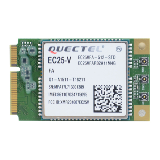
- Page 1 EC25-V User Manual LTE Module Series Rev. EC25-V_User_Manual_V1.0 Date: 2016-03-28 www.quectel.com...
- Page 2 QUECTEL OFFERS THIS INFORMATION AS A SERVICE TO ITS CUSTOMERS. THE INFORMATION PROVIDED IS BASED UPON CUSTOMERS’ REQUIREMENTS. QUECTEL MAKES EVERY EFFORT TO ENSURE THE QUALITY OF THE INFORMATION IT MAKES AVAILABLE. QUECTEL DOES NOT MAKE ANY WARRANTY AS TO THE INFORMATION CONTAINED HEREIN, AND DOES NOT ACCEPT ANY LIABILITY FOR ANY INJURY, LOSS OR DAMAGE OF ANY KIND INCURRED BY USE OF OR RELIANCE UPON THE INFORMATION.
-
Page 3: About The Document
LTE Module Series EC25-V User Manual About the Document History Revision Date Author Description V1.0 2016-03-28 Woody WU Initial EC25-V_User_Manual Confidential / Released 2 / 69... -
Page 4: Table Of Contents
LTE Module Series EC25-V User Manual Contents About the Document ........................... 2 Contents ............................... 3 Table Index ..............................5 Figure Index ..............................6 Introduction ............................7 1.1. Safety Information........................7 Product Concept ..........................9 2.1. General Description ........................9 2.2. - Page 5 LTE Module Series EC25-V User Manual 3.11. UART Interface ........................36 3.12. PCM and I2C Interface ......................38 3.13. ADC Function .......................... 41 3.14. Network Status Indication ......................41 3.15. STATUS ........................... 42 3.16. Behavior of the RI ........................43 GNSS Receiver ...........................
- Page 6 LTE Module Series EC25-V User Manual Table Index TABLE 1: EC25 SERIES FREQUENCY BANDS ....................9 TABLE 2: EC25 KEY FEATURES ........................10 TABLE 3: IO PARAMETERS DEFINITION ......................16 TABLE 4: PIN DESCRIPTION ........................... 16 TABLE 5: OVERVIEW OF OPERATING MODES ..................... 21 TABLE 6: VBAT AND GND PINS ........................
- Page 7 LTE Module Series EC25-V User Manual Figure Index FIGURE 1: FUNCTIONAL DIAGRAM ......................12 FIGURE 2: PIN ASSIGNMENT (TOP VIEW) ..................... 15 FIGURE 3: UART SLEEP APPLICATION ....................22 FIGURE 4: SLEEP APPLICATION WITH USB REMOTE WAKEUP ............23 FIGURE 5: SLEEP APPLICATION WITH RI ..................... 24 FIGURE 6: SLEEP APPLICATION WITHOUT SUSPEND FUNCTION ............
-
Page 8: Introduction
If not so, Quectel assumes no liability for the customer’s failure to comply with these precautions. - Page 9 LTE Module Series EC25-V User Manual Cellular terminals or mobiles operating over radio frequency signal and cellular network cannot be guaranteed to connect in all conditions, for example no mobile fee or with an invalid SIM card. While you are in this condition and need emergent help, please remember using emergency call.
-
Page 10: Product Concept
EC25-V User Manual Product Concept 2.1. General Description EC25 contains four variants: EC25-E, EC25-A, EC25-V and EC25-AUT. You can choose the dedicated type based on the region or operator. The following table shows the frequency bands of EC25 series modules. -
Page 11: Directives And Standards
LTE Module Series EC25-V User Manual 2.2. Directives and Standards 2.2.1. FCC Statement Any Changes or modifications not expressly approved by the party responsible for compliance could void the user’s authority to operate the equipment. This device complies with part 15 of the FCC Rules. Operation is subject to the following two conditions: (1) This device may not cause harmful interference, and (2) this device must accept any interference received, including interference that may cause undesired operation. - Page 12 LTE Module Series EC25-V User Manual Support master and slave mode, but must be the master in long frame sync Compliant with USB 2.0 specification (slave only); the data transfer rate can reach up to 480Mbps Used for AT command communication, data transmission, GNSS NMEA...
-
Page 13: Functional Diagram
LTE Module Series EC25-V User Manual 2.4. Functional Diagram The following figure shows a block diagram of EC25 and illustrates the major functional parts. Power management Baseband DDR+NAND flash Radio frequency Peripheral interface ANT_MAIN ANT_GNSS... -
Page 14: Evaluation Board
LTE Module Series EC25-V User Manual 2.5. Evaluation Board In order to help you to develop applications with EC25, Quectel supplies an evaluation board (EVB), USB data cable, earphone, antenna and other peripherals to control or test the module. EC25-V_User_Manual... -
Page 15: Application Interface
LTE Module Series EC25-V User Manual Application Interface 3.1. General Description EC25 is equipped with an 80-pin SMT pad plus 64-pin ground pads and reserved pads that can be connected to cellular application platform. Sub-interfaces included in these pads are described in detail in... -
Page 16: Figure 2: Pin Assignment (Top View)
LTE Module Series EC25-V User Manual WAKEUP_IN AP_READY RESERVED W_DISABLE# NET_MODE NET_STATUS ANT_MAIN VDD_EXT RESERVED RESERVED RESERVED RESERVED ANT_GNSS USIM_GND ADC0 ADC1 DBG_RXD DBG_TXD RESERVED I2C_SDA USIM_PRESENCE USIM_VDD I2C_SCL USIM_DATA RESERVED USIM_CLK RESERVED USIM_RST RESERVED RESERVED RESERVED Power Pins GND Pins... -
Page 17: Pin Description
LTE Module Series EC25-V User Manual 3.3. Pin Description The following tables show the EC25’s pin definition. Table 3: IO Parameters Definition Type Description Bidirectional input/output Digital input Digital output Power input Power output Analog input Analog output Open drain... - Page 18 LTE Module Series EC25-V User Manual 85~112 Turn on/off Pin Name Pin No. Description DC Characteristics Comment max=2.1V Turn on/off the PWRKEY min=1.3V module. max=0.5V max=2.1V RESET_N Reset the module. min=1.3V max=0.5V Status Indication Pin Name Pin No. Description DC Characteristics...
- Page 19 LTE Module Series EC25-V User Manual For 3.0V USIM: Vmax=3.05V Vmin=2.7V max=50mA For 1.8V USIM: max=0.6V min=1.2V max=0.45V min=1.35V Data signal of USIM USIM_DATA card. For 3.0V USIM: max=1.0V min=1.95V max=0.45V min=2.55V For 1.8V USIM: max=0.45V min=1.35V Clock signal of USIM USIM_CLK card.
- Page 20 LTE Module Series EC25-V User Manual 1.8V power domain. max=0.45V Clear to send. If unused, keep it min=1.35V open. min=-0.3V 1.8V power domain. max=0.6V Request to send. If unused, keep it min=1.2V open. max=2.0V 1.8V power domain. min=-0.3V Pull-up by default.
- Page 21 LTE Module Series EC25-V User Manual min=-0.3V 1.8V power domain. max=0.6V PCM_IN PCM data input. If unused, keep it min=1.2V open. max=2.0V 1.8V power domain. max=0.45V PCM_OUT PCM data output. If unused, keep it min=1.35V open. max=0.45V 1.8V power domain.
-
Page 22: Operating Modes
LTE Module Series EC25-V User Manual 1.8V power domain. min=-0.3V Pull-up by default. max=0.6V WAKEUP_IN Sleep mode control. Low level wakes up min=1.2V the module. If max=2.0V unused, keep it open. 1.8V power domain. min=-0.3V Pull-up by default. Airplane mode max=0.6V... -
Page 23: Power Saving
LTE Module Series EC25-V User Manual In this mode, the current consumption of the module will be reduced to the minimal level. Sleep Mode During this mode, the module can still receive paging message, SMS, voice call and TCP/UDP data from the network normally. -
Page 24: Usb Application With Usb Remote Wakeup Function
LTE Module Series EC25-V User Manual Refer to AT command AT+QCFG=“apready” for details. 3.5.1.2. USB Application with USB Remote Wakeup Function If host supports USB suspend/resume and remote wakeup function, the following part will show the sleep application. There are three preconditions to let the module enter into the sleep mode. -
Page 25: Usb Application Without Usb Suspend Function
LTE Module Series EC25-V User Manual state. The following figure shows the connection between the module and the host. Module Host USB_VBUS USB_DP USB_DP USB_DM USB_DM GPIO AP_READY EINT Figure 5: Sleep Application with RI Sending data to EC25 through USB will wake up the module. -
Page 26: Airplane Mode
LTE Module Series EC25-V User Manual Opening power switch to supply power to USB_VBUS will wake up the module. NOTE You should pay attention to the level match shown in dotted line between module and host. Refer to document [1] for more details about EC25 power management application. -
Page 27: Decrease Voltage Drop
LTE Module Series EC25-V User Manual Table 6: VBAT and GND Pins Pin Name Pin No. Description Min. Typ. Max. Unit Power supply for module RF VBAT_RF 57, 58 part. Power supply for module VBAT_BB 59, 60 baseband part. 8, 9, 19, 22, 36, 46, 48, 50~54, Ground. -
Page 28: Reference Design For Power Supply
LTE Module Series EC25-V User Manual VBAT VBAT_RF VBAT_BB 100nF 10pF 100uF 33pF 100uF 100nF 33pF 10pF 5.1V Module Figure 8: Star Structure of the Power Supply 3.6.3. Reference Design for Power Supply The power design for the module is very important, as the performance of the module largely depends on the power source. -
Page 29: Monitor The Power Supply
LTE Module Series EC25-V User Manual 3.6.4. Monitor the Power Supply You can use the AT+CBC command to monitor the VBAT_BB voltage value. For more details, please refer to document [2]. 3.7. Turn on and off Scenarios 3.7.1. Turn on Module Using the PWRKEY The following table shows the pin definition of PWRKEY. -
Page 30: Figure 11: Turn On The Module Using Keystroke
LTE Module Series EC25-V User Manual PWRKEY Close to S1 Figure 11: Turn on the Module Using Keystroke The turn on scenario is illustrated in the following figure. NOTE VBAT ≥ 100ms ≥ 1.3V PWRKEY ≤ 0.5V RESET_N STATUS (OD) -
Page 31: Turn Off Module
LTE Module Series EC25-V User Manual 3.7.2. Turn off Module The following procedures can be used to turn off the module: Normal power down procedure: Turn off the module using the PWRKEY pin. Normal power down procedure: Turn off the module using command AT+QPOWD. -
Page 32: Table 8: Reset_N Pin Description
LTE Module Series EC25-V User Manual Table 8: RESET_N Pin Description Pin Name Pin No. Description DC Characteristics Comment max=2.1V RESET_N Reset the module. min=1.3V max=0.5V The recommended circuit is similar to the PWRKEY control circuit. You can use an open drain/collector driver or button to control the RESET_N. -
Page 33: Usim Card Interface
LTE Module Series EC25-V User Manual VBAT ≤Treset_max ≥Treset_min ≥ 1.3V RESET_N ≤ 0.5V Module RUNNING RESETTING RUNNING Status Figure 16: Timing of Resetting Module NOTES Use the RESET_N only when turning off the module by the command AT+QPOWD and the PWRKEY pin failed. -
Page 34: Figure 17: Reference Circuit Of 8-Pin Usim Connector
LTE Module Series EC25-V User Manual EC25 supports USIM card hot-plug via the USIM_PRESENCE pin. It supports low level and high level detections, which is disabled by default. For details, refer to document [2] about the command AT+QSIMDET. The following figure shows the reference design of the 8-pin USIM connector. -
Page 35: Usb Interface
LTE Module Series EC25-V User Manual criteria below in the USIM circuit design: Keep layout of USIM card as close as possible to the module. Assure the length of trace is less than 200mm. Keep USIM card signal away from RF and VBAT alignment. -
Page 36: Figure 19: Reference Circuit Of Usb Application
LTE Module Series EC25-V User Manual Test Points Minimize this stub Module NM_0R NM_0R ESD Array USB_VBUS USB_DM USB_DM USB_DP USB_DP Close to Module Figure 19: Reference Circuit of USB Application In order to meet USB data line signal integrity, components R1, R2, R3 and R4 must be placed close to the module, and then these resistors should be placed close to each other. -
Page 37: Uart Interface
LTE Module Series EC25-V User Manual 3.11. UART Interface The module provides two UART interfaces: main UART interface and debug UART interface. The following shows the different features. Main UART interface supports 9600, 19200, 38400, 57600, 115200, 230400, 460800, 921600bps ... -
Page 38: Table 13: Logic Levels Of Digital I/O
LTE Module Series EC25-V User Manual Table 13: Logic Levels of Digital I/O Parameter Min. Max. Unit -0.3 0.45 1.35 The module provides 1.8V UART interface. A level translator should be used if your application is equipped with a 3.3V UART interface. A level translator TXS0108EPWR provided by Texas Instrument is recommended. -
Page 39: Pcm And I2C Interface
LTE Module Series EC25-V User Manual 4.7K VDD_EXT VDD_EXT Module MCU/ARM /TXD /RXD VDD_EXT VCC_MCU 4.7K /RTS /CTS GPIO EINT GPIO Figure 21: Reference Circuit with Transistor Circuit NOTE Transistor circuit solution is not suitable for high baud rates exceeding 460Kbps. -
Page 40: Table 14: Pin Definition Of Pcm And I2C Interface
LTE Module Series EC25-V User Manual 125us PCM_CLK PCM_SYNC PCM_OUT PCM_IN Figure 22: Primary Mode Timing 125us PCM_CLK PCM_SYNC PCM_OUT PCM_IN Figure 23: Auxiliary Mode Timing The following table shows the pin definition of PCM and I2C interface which can be applied on audio codec design. -
Page 41: Figure 24: Reference Circuit Of Pcm Application With Audio Codec
LTE Module Series EC25-V User Manual PCM_OUT PCM data output 1.8V power domain PCM_SYNC PCM data frame sync signal 1.8V power domain PCM_CLK PCM data bit clock 1.8V power domain I2C_SCL I2C serial clock Require external pull-up to 1.8V I2C_SDA I2C serial data Require external pull-up to 1.8V... -
Page 42: Adc Function
LTE Module Series EC25-V User Manual 3.13. ADC Function The module provides two analog-to-digital converters (ADC). Using AT command AT+QADC=0 can read the voltage value on ADC0 pin. Using AT command AT+QADC=1 can read the voltage value on ADC1 pin. For more details of these AT commands, please refer to document [2]. -
Page 43: Status
LTE Module Series EC25-V User Manual mode. Indicate the module network activity NET_STATUS 1.8V power domain status. Table 18: Working State of the Network Indicator Pin Name Status Description Always High Registered in LTE network NET_MODE Always Low Others Flicker slowly (200ms High/1800ms Low) -
Page 44: Behavior Of The Ri
LTE Module Series EC25-V User Manual Table 19: Pin Definition of STATUS Pin Name Pin No. Description Comment STATUS Indicate the module operation status Require external pull-up The following figure shows different design circuit of STATUS, you can choose either one according to your application demands. -
Page 45: Table 20: Behavior Of The Ri
LTE Module Series EC25-V User Manual Table 20: Behavior of the RI State Response Idle RI keeps high level RI outputs 120ms low pulse when new URC returns The RI behavior can be changed by command AT+QCFG=“urc/ri/ring”. Refer to document [2] for details. -
Page 46: Gnss Receiver
LTE Module Series EC25-V User Manual GNSS Receiver 4.1. General Description EC25 includes a fully integrated global navigation satellite system solution that supports Gen8C-Lite of Qualcomm (GPS, GLONASS, BeiDou, Galileo and QZSS). EC25 supports standard NMEA-0183 protocol, and outputs NMEA sentences with 1Hz via USB interface by default. -
Page 47: Layout Guideline
LTE Module Series EC25-V User Manual Autonomous Hot start @open sky XTRA enabled Accuracy Autonomous CEP-50 (GNSS) @open sky NOTES Tracking sensitivity: the lowest GPS signal value at the antenna port for which the module can keep on positioning for 3 minutes. -
Page 48: Antenna Interface
LTE Module Series EC25-V User Manual Antenna Interface EC25 antenna interface includes a main antenna, an Rx-diversity antenna which is used to resist the fall of signals caused by high speed movement and multipath effect, and a GNSS antenna. The antenna interface has an impedance of 50ohm. -
Page 49: Gnss Antenna Interface
LTE Module Series EC25-V User Manual Main Module antenna ANT_MAIN Diversity antenna ANT_DIV Figure 27: Reference Circuit of Antenna Interface NOTES Keep a proper distance between the main antenna and the Rx-diversity antenna to improve the receiving sensitivity. ANT_DIV function is enabled by default. Use the AT command can disable AT+QCFG="diversity",0... -
Page 50: Antenna Installation
LTE Module Series EC25-V User Manual Table 25: GNSS Frequency Type Frequency Unit GPS/Galileo/QZSS 1575.42 ± 1.023 GLONASS 1597.5 ~ 1605.8 BeiDou 1561.098 ± 2.046 The reference design of GNSS antenna is shown as below. GNSS 0.1uF Antenna Module 47nH... -
Page 51: Install The Antenna With Rf Connector
LTE Module Series EC25-V User Manual Frequency range: 1561 - 1615MHz Polarization: RHCP or linear VSWR: < 2 (Typ.) Passive antenna gain: > 0dBi GNSS Active antenna noise figure: < 1.5dB Active antenna gain: > -2dBi Active antenna embedded LNA gain: 20dB (Typ.) Active antenna total gain: >... -
Page 52: Figure 30: Mechanicals Of Uf.l-Lp Connectors
LTE Module Series EC25-V User Manual You can use U.FL-LP serial connector listed in the following figure to match the UF.L-R-SMT. Figure 30: Mechanicals of UF.L-LP Connectors EC25-V_User_Manual Confidential / Released 51 /... -
Page 53: Figure 31: Space Factor Of Mated Connector (Unit: Mm)
LTE Module Series EC25-V User Manual The following figure describes the space factor of mated connector. Figure 31: Space Factor of Mated Connector (Unit: mm) For more details, please visit http://www.hirose.com. EC25-V_User_Manual Confidential / Released 52 /... -
Page 54: Electrical, Reliability And Radio Characteristics
LTE Module Series EC25-V User Manual Electrical, Reliability and Radio Characteristics 6.1. Absolute Maximum Ratings Absolute maximum ratings for power supply and voltage on digital and analog pins of the module are listed in the following table. Table 27: Absolute Maximum Ratings Parameter Min. -
Page 55: Operating Temperature
LTE Module Series EC25-V User Manual Parameter Description Conditions Min. Typ. Max. Unit VBAT_RF min/max values, including voltage drop, ripple and spikes. Voltage drop during Maximum power control transmitting burst level on GSM900. Peak supply current Maximum power control (during transmission VBAT level on GSM900. -
Page 56: Rf Receiving Sensitivity
LTE Module Series EC25-V User Manual Table 30: Conducted RF Output Power Frequency Max. Min. LTE FDD B4/B13 23dBm±2dB <-44dBm 6.6. RF Receiving Sensitivity This information will be added in future version of this document. 6.7. Electrostatic Discharge The module is not protected against electrostatics discharge (ESD) in general. Consequently, it is subject to ESD handling precautions that typically apply to ESD sensitive components. -
Page 57: Mechanical Dimensions
LTE Module Series EC25-V User Manual Mechanical Dimensions This chapter describes the mechanical dimensions of the module. All dimensions are measured in mm. 7.1. Mechanical Dimensions of the Module (32+/-0.15) 2.4+/-0.2 Figure 32: Module Top and Side Dimensions EC25-V_User_Manual Confidential / Released... -
Page 58: Figure 33: Module Bottom Dimensions (Bottom View)
LTE Module Series EC25-V User Manual 32.0 Figure 33: Module Bottom Dimensions (Bottom View) EC25-V_User_Manual Confidential / Released 57 /... -
Page 59: Footprint Of Recommendation
LTE Module Series EC25-V User Manual 7.2. Footprint of Recommendation Keepout area 32.0 Figure 34: Recommended Footprint (Top View) NOTES Pads 73~84 should not be designed. In order to maintain the module, keep about 3mm between the module and other components in the host PCB. -
Page 60: Top View Of The Module
LTE Module Series EC25-V User Manual 7.3. Top View of the Module Figure 35: Top View of the Module 7.4. Bottom View of the Module Figure 36: Bottom View of the Module EC25-V_User_Manual Confidential / Released 59 /... -
Page 61: Storage And Manufacturing
LTE Module Series EC25-V User Manual Storage and Manufacturing 8.1. Storage EC25 is stored in a vacuum-sealed bag. The restrictions of storage condition are shown as below. 1. Shelf life in sealed bag is 12 months at < 40ºC/90%RH. After this bag is opened, devices that will be subjected to reflow soldering or other high temperature processes must be: Mounted within 72 hours at factory conditions of ≤... -
Page 62: Packaging
LTE Module Series EC25-V User Manual suggested that the module should be mounted after the first panel has been reflowed. The following picture is the actual diagram which we have operated. ºC Preheat Heating Cooling Liquids Temperature ºC 40s~60s ºC... -
Page 63: Figure 38: Carrier Tape
LTE Module Series EC25-V User Manual 44.00 ±0.1 0.35± 0.05 ±0.1 2.00 ±0.1 4.00 ±0.15 ±0.15 32.5 ±0.15 ±0.15 33.5 32.5± 0.15 33.5± 0.15 48.5 Cover tape Direction of feed +0.20 44.5 -0.00 Figure 38: Carrier Tape EC25-V_User_Manual Confidential / Released... -
Page 64: Appendix A Reference
LTE Module Series EC25-V User Manual Appendix A Reference Table 32: Related Documents Document Name Remark Quectel_EC25_Power_Management_Application_ EC25 Power Management Application Note Note Quectel_EC25_AT_Commands_Manual EC25 AT Commands Manual Quectel_EC25_GNSS_AT_Commands_Manual EC25 GNSS AT Commands Manual Quectel_Module_Secondary_SMT_User_Guide Module Secondary SMT User Guide... - Page 65 LTE Module Series EC25-V User Manual Enhanced Full Rate Electrostatic Discharge Frequency Division Duplex Full Rate GLObalnaya NAvigatsionnaya Sputnikovaya Sistema, the Russian Global GLONASS Navigation Satellite System GMSK Gaussian Minimum Shift Keying GNSS Global Navigation Satellite System Global Positioning System...
- Page 66 LTE Module Series EC25-V User Manual Point-to-Point Protocol Quadrature Amplitude Modulation QPSK Quadrature Phase Shift Keying Radio Frequency RHCP Right Hand Circularly Polarized Receive Subscriber Identification Module Short Message Service Time Division Duplexing TDMA Time Division Multiple Access TD-SCDMA Time Division-Synchronous Code Division Multiple Access...
- Page 67 VSWR Voltage Standing Wave Ratio Directives and Standards The EC25-V module is designed to comply with the FCC statements. FCC ID: XMR201607EC25V, The Host system using EC25-V, should have label indicated FCC ID: XMR201607EC25V. FCC Radiation Exposure Statement This equipment complies with FCC radiation exposure limits set forth for an uncontrolled environment .This equipment should be installed and operated with minimum distance 20 cm between...
Need help?
Do you have a question about the EC25-V and is the answer not in the manual?
Questions and answers