
Related Manuals for Quectel EG25-G


Summary of Contents for Quectel EG25-G
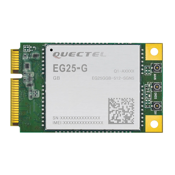
- Page 1 EG25-G Hardware Design LTE Module Series Rev. EG25-G_Hardware_Design_V1.0 Date: 2018-12-12 Status: Released www.quectel.com...
- Page 2 QUECTEL OFFERS THE INFORMATION AS A SERVICE TO ITS CUSTOMERS. THE INFORMATION PROVIDED IS BASED UPON CUSTOMERS’ REQUIREMENTS. QUECTEL MAKES EVERY EFFORT TO ENSURE THE QUALITY OF THE INFORMATION IT MAKES AVAILABLE. QUECTEL DOES NOT MAKE ANY WARRANTY AS TO THE INFORMATION CONTAINED HEREIN, AND DOES NOT ACCEPT ANY LIABILITY FOR ANY INJURY, LOSS OR DAMAGE OF ANY KIND INCURRED BY USE OF OR RELIANCE UPON THE INFORMATION.
-
Page 3: About The Document
LTE Module Series EG25-G Hardware Design About the Document History Revision Date Author Description Lorry XU/ 2018-12-12 Initial Harry HUANG EG25-G_Hardware_Design 2 / 100... -
Page 4: Table Of Contents
LTE Module Series EG25-G Hardware Design Contents About the Document ........................... 2 Contents ............................... 3 Table Index ..............................5 Figure Index ..............................7 Introduction ............................9 Safety Information........................10 1.1. Product Concept ..........................11 General Description ......................... 11 2.1. Key Features ........................... 12 2.2. - Page 5 LTE Module Series EG25-G Hardware Design SGMII Interface ........................54 3.15. ADC Interfaces ........................56 3.16. Network Status Indication ......................57 3.17. STATUS ........................... 58 3.18. Behaviors of RI ........................59 3.19. USB_BOOT Interface ......................60 3.20. GNSS Receiver ........................... 61 General Description .........................
- Page 6 TABLE 33: OPERATION AND STORAGE TEMPERATURES ................73 TABLE 34: EG25-G CURRENT CONSUMPTION ..................... 74 TABLE 35: GNSS CURRENT CONSUMPTION OF EG25-G MODULE ............78 TABLE 36: RF OUTPUT POWER ........................79 TABLE 37: EG25-G CONDUCTED RF RECEIVING SENSITIVITY ..............79 TABLE 38: ELECTROSTATICS DISCHARGE CHARACTERISTICS (25ºC, 45% RELATIVE HUMIDITY) ..
- Page 7 LTE Module Series EG25-G Hardware Design TABLE 42: DESCRIPTION OF DIFFERENT CODING SCHEMES ..............96 TABLE 43: GPRS MULTI-SLOT CLASSES ...................... 97 TABLE 44: EDGE MODULATION AND CODING SCHEMES ................99 EG25-G_Hardware_Design 6 / 100...
- Page 8 LTE Module Series EG25-G Hardware Design Figure Index FIGURE 1: FUNCTIONAL DIAGRAM ....................... 15 FIGURE 2: PIN ASSIGNMENT (TOP VIEW)..................... 17 FIGURE 3: SLEEP MODE APPLICATION VIA UART ..................30 FIGURE 4: SLEEP MODE APPLICATION WITH USB REMOTE WAKEUP ............ 31 FIGURE 5: SLEEP MODE APPLICATION WITH RI ..................
- Page 9 LTE Module Series EG25-G Hardware Design FIGURE 38: DIMENSIONS OF THE U.FL-R-SMT CONNECTOR (UNIT: MM) ..........70 FIGURE 39: MECHANICALS OF U.FL-LP CONNECTORS ................70 FIGURE 40: SPACE FACTOR OF MATED CONNECTOR (UNIT: MM) ............71 FIGURE 41: REFERENCED HEATSINK DESIGN (HEATSINK AT THE TOP OF THE MODULE) ....82 FIGURE 42: REFERENCED HEATSINK DESIGN (HEATSINK AT THE BACKSIDE OF CUSTOMERS’...
-
Page 10: Introduction
This document can help customers quickly understand module interface specifications, electrical and mechanical details as well as other related information of EG25-G module. To facilitate its application in different fields, relevant reference design is also provided for customers’ reference. Associated with application note and user guide, customers can use the module to design and set up mobile applications easily. -
Page 11: Safety Information
EG25-G module. Manufacturers of the cellular terminal should send the following safety information to users and operating personnel, and incorporate these guidelines into all manuals supplied with the product. If not so, Quectel assumes no liability for customers’ failure to comply with these precautions. -
Page 12: Product Concept
EG25-G module includes Data-only and Telematics versions. Data-only version does not support voice function, while Telematics version supports it. With a compact profile of 29.0mm × 32.0mm × 2.4mm, EG25-G can meet almost all requirements for M2M applications such as automotive, metering, tracking system, security, router, wireless POS, mobile computing device, PDA phone, tablet PC, etc. -
Page 13: Key Features
LTE Module Series EG25-G Hardware Design 2.2. Key Features The following table describes the detailed features of EG25-G module. Table 2: Key Features of EG25 -G Module Feature Details Supply voltage: 3.3V~4.3V Power Supply Typical supply voltage: 3.8V Class 4 (33dBm±2dB) for GSM850 Class 4 (33dBm±2dB) for EGSM900... - Page 14 LTE Module Series EG25-G Hardware Design Support TCP/UDP/PPP/FTP/HTTP/NTP/PING/QMI/NITZ/CMUX*/HTTPS*/ SMTP/MMS*/FTPS*/SMTPS*/SSL*/FILE* protocols Internet Protocol Support PAP (Password Authentication Protocol) and CHAP (Challenge Features Handshake Authentication Protocol) protocols which are usually used for PPP connections Text and PDU mode Point to point MO and MT...
-
Page 15: Functional Diagram
When the temperature returns to normal operation temperature levels, the module will meet 3GPP specifications again. 3. “*” means under development. 2.3. Functional Diagram The following figure shows a block diagram of EG25-G and illustrates the major functional parts. Power management ... -
Page 16: Evaluation Board
NOTE “*” means under development. 2.4. Evaluation Board In order to help customers develop applications with EG25-G, Quectel supplies an evaluation board (EVB), USB to RS-232 converter cable, earphone, antenna and other peripherals to control or test the module. EG25-G_Hardware_Design... -
Page 17: Application Interfaces
LTE Module Series EG25-G Hardware Design Application Interfaces 3.1. General Description EG25-G is equipped with 144 LGA pads that can be connected to cellular application platform. Sub-interfaces included in these pads are described in detail in the following chapters: Power supply ... -
Page 18: Pin Assignment
LTE Module Series EG25-G Hardware Design 3.2. Pin Assignment The following figure shows the pin assignment of EG25-G module. WAKEUP_IN AP_READY RESERVED W_DISABLE# NET_MODE NET_ST ATUS ANT_MAIN VDD_EXT 14 1 14 4 RESERVED RESERVED 14 2 14 3 RESERVED RESERVED... -
Page 19: Pin Description
PCB decal, and these pins should be served as a keepout area. “*” means under development. 3.3. Pin Description The following tables show the pin definition of EG25-G modules. Table 3: I/O Parameters Definition Type... - Page 20 LTE Module Series EG25-G Hardware Design Power supply for Provide 1.8V for Vnorm=1.8V external GPIO’s pull up VDD_EXT external circuit max=50mA circuits. If unused, keep it open. 8, 9, 19, 22, 36, 46, 48, 50~54, Ground 56, 72, 85~112 Turn on/off Pin Name Pin No.
- Page 21 LTE Module Series EG25-G Hardware Design Require differential Compliant with USB USB differential data impedance of 90Ω. USB_DM 2.0 standard bus (-) If unused, keep it specification. open. (U)SIM Interface Pin Name Pin No. Description DC Characteristics Comment Specified ground for...
- Page 22 LTE Module Series EG25-G Hardware Design min=-0.3V 1.8V power domain. USIM_ (U)SIM card max=0.6V If unused, keep it PRESENCE insertion detection min=1.2V open. max=2.0V Main UART Interface Pin Name Pin No. Description DC Characteristics Comment 1.8V power domain. max=0.45V Ring indicator If unused, keep it min=1.35V...
- Page 23 LTE Module Series EG25-G Hardware Design max=2.0V ADC Interfaces Pin Name Pin No. Description DC Characteristics Comment General purpose Voltage range: If unused, keep it ADC0 analog to digital 0.3V to VBAT_BB open. converter General purpose Voltage range: If unused, keep it...
- Page 24 LTE Module Series EG25-G Hardware Design keep it open. SD Card Interface Pin Name Pin No. Description DC Characteristics Comment 1.8V signaling: max=0.45V min=1.4V min=-0.3V SDIO signal level can max=0.58V be selected min=1.27V according to SD card max=2.0V supported level,...
- Page 25 LTE Module Series EG25-G Hardware Design max=0.38V min=2.01V min=-0.3V max=0.76V min=1.72V max=3.34V 1.8V signaling: max=0.45V min=1.4V min=-0.3V SDIO signal level can max=0.58V be selected min=1.27V according to SD card max=2.0V supported level, SD card SDIO bus SDC2_ please refer to SD 3.0...
- Page 26 LTE Module Series EG25-G Hardware Design max=3.34V min=-0.3V 1.8V power domain. SD card insertion max=0.6V SD_INS_ If unused, keep it detect min=1.2V open. max=2.0V 1.8V/2.85V configurable. SD card SDIO bus Cannot be used for max=50mA VDD_SDIO pull-up power SD card power.
- Page 27 LTE Module Series EG25-G Hardware Design min=1.2V max=2.0V 1.8V power domain. WLAN SDIO bus max=0.45V SDC1_CLK If unused, keep it clock min=1.35V open. 1.8V power domain. WLAN SDIO bus max=0.45V SDC1_CMD If unused, keep it command min=1.35V open. min=-0.3V 1.8V power domain.
- Page 28 LTE Module Series EG25-G Hardware Design open. 1.8V power domain. BT function control max=0.45V BT_EN* If unused, keep it via FC20 module min=1.35V open. SGMII Interface Pin Name Pin No. Description DC Characteristics Comment For 1.8V: max=0.45V 1.8V/2.85V power min=1.4V domain.
- Page 29 LTE Module Series EG25-G Hardware Design SGMII receiving If unused, keep it SGMII_RX_M - minus open. 1.8V/2.85V SGMII MDIO pull-up configurable. USIM2_VDD power source If unused, keep it open. RF Interface Pin Name Pin No. Description DC Characteristics Comment If unused, keep it...
-
Page 30: Operating Modes
116, 117, 140~144 NOTES 1. Pads 24~27 are multiplexing pins used for audio design on EG25-G module and BT function on FC20 module. 2. “*” means under development. 3.4. Operating Modes The table below briefly summarizes the various operating modes referred in the following chapters. -
Page 31: Power Saving
Driving the host DTR to low level will wake up the module. When EG25-G has a URC to report, RI signal will wake up the host. Please refer to Chapter 3.19 for details about RI behaviors. AP_READY will detect the sleep state of the host (can be configured to high level or low level detection). -
Page 32: Usb Application With Usb Remote Wakeup Function
Sending data to EG25-G through USB will wake up the module. When EG25-G has a URC to report, the module will send remote wake-up signals via USB bus so as to wake up the host. 3.5.1.3. USB Application with USB Suspension/Resume and RI Function If the host supports USB suspension and resume, but does not support remote wake-up function, the RI signal is needed to wake up the host. -
Page 33: Usb Application Without Usb Suspension Function
Sending data to EG25-G through USB will wake up the module. When EG25-G has a URC to report, RI signal will wake up the host. 3.5.1.4. USB Application without USB Suspension Function If the host does not support USB suspension function, USB_VBUS should be disconnected via an additional control circuit to let the module enter into sleep mode. -
Page 34: Airplane Mode
2. The execution of AT+CFUN command will not affect GNSS function. 3.6. Power Supply 3.6.1. Power Supply Pins EG25-G provides four VBAT pins to connect with the external power supply, and there are two separate voltage domains for VBAT. ... -
Page 35: Decrease Voltage Drop
LTE Module Series EG25-G Hardware Design The following table shows the details of VBAT pins and ground pins. Table 6: VBAT and GND Pins Pin Name Pin No. Description Min. Typ. Max. Unit Power supply for module’s VBAT_RF 57, 58 RF part Power supply for module’s... -
Page 36: Reference Design For Power Supply
LTE Module Series EG25-G Hardware Design VBAT VBAT_RF VBAT_BB 100nF 10pF 33pF 100uF 100nF 33pF 10pF 100uF Module Figure 8: Star Structure of the Power Supply 3.6.3. Reference Design for Power Supply Power design for the module is very important, as the performance of the module largely depends on the power source. -
Page 37: Monitor The Power Supply
Qualcomm chipset. When EG25-G is in power-down mode, it can be turned on to normal mode by driving the PWRKEY pin to a low level for at least 500ms. It is recommended to use an open drain/collector driver to control the PWRKEY. -
Page 38: Figure 11: Turn On The Module By Using Keystroke
LTE Module Series EG25-G Hardware Design The other way to control the PWRKEY is using a button directly. When pressing the key, electrostatic strike may generate from finger. Therefore, a TVS component is indispensable to be placed nearby the button for ESD protection. A reference circuit is shown in the following figure. -
Page 39: Turn Off Module
LTE Module Series EG25-G Hardware Design NOTE Please make sure that VBAT is stable before pulling down PWRKEY pin. The time between them should be no less than 30ms. 3.7.2. Turn off Module The following procedures can be used to turn off the module: ... -
Page 40: Reset The Module
LTE Module Series EG25-G Hardware Design NOTES 1. In order to avoid damaging internal flash, please do not switch off the power supply when the module works normally. Only after the module is shut down by PWRKEY or AT command, then the power supply can be cut off. -
Page 41: U)Sim Interface
LTE Module Series EG25-G Hardware Design RESET_N Close to S2 Figure 15: Reference Circuit of RESET_N by Using Button The reset scenario is illustrated in the following figure. VBAT ≤460ms ≥150ms ≥1.3V RESET_N ≤0.5V Module Running Resetting Restart Status Figure 16: Timing of Resetting Module NOTES Use RESET_N only when failed to turn off the module by AT+QPOWD command and PWRKEY pin. -
Page 42: Table 9: Pin Definition Of (U)Sim Interface
Specified ground for (U)SIM USIM_GND card EG25-G supports (U)SIM card hot-plug via the USIM_PRESENCE pin. The function supports low level and high level detections, and is disabled by default. Please refer to document [2] for more details about AT+QSIMDET command. -
Page 43: Figure 18: Reference Circuit Of (U)Sim Interface With A 6-Pin (U)Sim Card Connector
LTE Module Series EG25-G Hardware Design USIM_VDD 100nF USIM_GND (U)SIM Card Connector USIM_VDD USIM_RST Module USIM_CLK USIM_DATA 33pF 33pF 33pF Figure 18: Reference Circuit of (U)SIM Interface with a 6-Pin (U)SIM Card Connector In order to enhance the reliability and availability of the (U)SIM card in customers’ applications, please follow the criteria below in (U)SIM circuit design: ... -
Page 44: Usb Interface
EG25-G Hardware Design 3.10. USB Interface EG25-G contains one integrated Universal Serial Bus (USB) interface which complies with the USB 2.0 specification and supports high-speed (480Mbps) and full-speed (12Mbps) modes. The USB interface is used for AT command communication, data transmission, GNSS NMEA sentences output, software debugging, firmware upgrade and voice over USB*. -
Page 45: Uart Interfaces
Keep the ESD protection components to the USB connector as close as possible. NOTES EG25-G module can only be used as a slave device. “*” means under development. 3.11. UART Interfaces The module provides two UART interfaces: the main UART interface and the debug UART interface. The following shows their features. -
Page 46: Table 11: Pin Definition Of Main Uart Interface
LTE Module Series EG25-G Hardware Design Table 11: Pin Definition of Main UART Interface Pin Name Pin No. Description Comment Ring indicator Data carrier detection Clear to send Request to send 1.8V power domain Data terminal ready, sleep mode control... -
Page 47: Figure 20: Reference Circuit With Translator Chip
LTE Module Series EG25-G Hardware Design VDD_EXT VCCA VCCB VDD_MCU 0.1uF 0.1uF RI_MCU DCD_MCU Translator CTS_MCU RTS_MCU DTR_MCU TXD_MCU RXD_MCU Figure 20: Reference Circuit with Translator Chip Please visit http://www.ti.com for more information. Another example with transistor translation circuit is shown as below. The circuit design of dotted line section can refer to the design of solid line section, in terms of both module’s input and output circuit... -
Page 48: Pcm And I2C Interfaces
LTE Module Series EG25-G Hardware Design 3.12. PCM and I2C Interfaces EG25-G provides one Pulse Code Modulation (PCM) digital interface for audio design, which supports the following modes and one I2C interface: Primary mode (short frame synchronization, works as both master and slave) Auxiliary mode (long frame synchronization, works as master only) ... -
Page 49: Table 14: Pin Definition Of Pcm And I2C Interfaces
LTE Module Series EG25-G Hardware Design 125us PCM_CLK PCM_SYNC PCM_OUT PCM_IN Figure 23: Auxiliary Mode Timing The following table shows the pin definition of PCM and I2C interfaces which can be applied on audio codec design. Table 14: Pin Definition of PCM and I2C Interfaces Pin Name Pin No. -
Page 50: Sd Card Interface
NOTES It is recommended to reserve an RC (R=22Ω, C=22pF) circuits on the PCM lines, especially for PCM_CLK. EG25-G works as a master device pertaining to I2C interface. 3.13. SD Card Interface EG25-G supports SDIO 3.0 interface for SD card. -
Page 51: Figure 25: Reference Circuit Of Sd Card
LTE Module Series EG25-G Hardware Design SDC2_CMD SD card SDIO bus command 1.8V/2.85V configurable. Cannot be used for SD VDD_SDIO SD card SDIO bus pull up power card power. If unused, keep it open. 1.8V power domain. SD_INS_DET SD card insertion detection If unused, keep it open. -
Page 52: Wireless Connectivity Interfaces
23mm. 3.14. Wireless Connectivity Interfaces EG25-G supports a low-power SDIO 3.0 interface for WLAN and a UART/PCM interface for BT. The following table shows the pin definition of wireless connectivity interfaces. Table 16: Pin Definition of Wireless Connectivity Interfaces Pin Name Pin No. - Page 53 PCM_CLK PCM data bit clock 1.8V power domain BT function control via FC20 1.8V power domain. BT_EN* module. Active high. The following figure shows a reference design of wireless connectivity interfaces with Quectel FC20 module. EG25-G_Hardware_Design 52 / 100...
-
Page 54: Wlan Interface
NOTES FC20 module can only be used as a slave device. When BT function is enabled on EG25-G module, PCM_SYNC and PCM_CLK pins are only used to output signals. Pads 24~27 are multiplexing pins used for audio design on EG25-G module and BT function on FC20 module. -
Page 55: Bt Interface
Further information about BT interface will be added in future version of this document. NOTE “*” means under development. 3.15. SGMII Interface EG25-G includes an integrated Ethernet MAC with an SGMII interface and two management interfaces, and key features of the SGMII interface are shown below: IEEE802.3 compliance ... -
Page 56: Table 17: Pin Definition Of Sgmii Interface
PHY side. SGMII_TX_P 124 SGMII transmission-plus SGMII_RX_P 125 SGMII receiving-plus Connect with a 0.1uF capacitor, and close to EG25-G module. SGMII_RX_M 126 SGMII receiving-minus The following figure shows the simplified block diagram for Ethernet application. SGMII Ethernet... -
Page 57: Adc Interfaces
LTE Module Series EG25-G Hardware Design The following figure shows a reference design of SGMII interface with PHY AR8033 application. Module AR8033 VDD_EXT 1.5K USIM2_VDD EPHY_INT_N EPHY_RST_N RSTN Control SGMII_MDATA MDIO SGMII_MCLK USIM2_VDD USIM2_VDD Close to Module 0.1uF SGMII_RX_P 0.1uF... -
Page 58: Network Status Indication
LTE Module Series EG25-G Hardware Design Table 18: Pin Definition of ADC Interfaces Pin Name Pin No. Description General purpose analog to digital converter ADC0 General purpose analog to digital converter ADC1 The following table describes the characteristic of the ADC function. -
Page 59: Status
LTE Module Series EG25-G Hardware Design Table 21: Working State of the Network Connection Status/Activity Indicator Pin Name Logic Level Changes Network Status Always High Registered on LTE network NET_MODE Always Low Others Flicker slowly (200ms High/1800ms Low) Network searching... -
Page 60: Behaviors Of Ri
LTE Module Series EG25-G Hardware Design Table 22: Pin Definition of STATUS Pin Name Pin No. Description Comment An external pull-up resistor STATUS Indicate the module operation status is required. If unused, keep it open. The following figure shows different circuit designs of STATUS, and customers can choose either one according to customers’... -
Page 61: Usb_Boot Interface
3.20. USB_BOOT Interface EG25-G provides a USB_BOOT pin. Customers can pull up USB_BOOT to VDD_EXT before powering on the module, thus the module will enter into emergency download mode when powered on. In this mode, the module supports firmware upgrade over USB interface. -
Page 62: Gnss Receiver
EG25-G supports standard NMEA-0183 protocol, and outputs NMEA sentences at 1Hz data update rate via USB interface by default. By default, EG25-G GNSS engine is switched off. It has to be switched on via AT command. For more details about GNSS engine technology and configurations, please refer to document [3]. -
Page 63: Layout Guidelines
LTE Module Series EG25-G Hardware Design @open sky XTRA enabled Accuracy Autonomous CEP-50 <4 (GNSS) @open sky NOTES Tracking sensitivity: the lowest GNSS signal value at the antenna port on which the module can keep on positioning for 3 minutes. -
Page 64: Antenna Interfaces
EG25-G Hardware Design Antenna Interfaces EG25-G antenna interfaces include a main antenna interface, an Rx-diversity antenna interface which is used to resist the fall of signals caused by high speed movement and multipath effect, and a GNSS antenna interface. The impedance of the antenna port is 50Ω. - Page 65 LTE Module Series EG25-G Hardware Design WCDMA B2 1850~1910 1930~1990 WCDMA B4 1710~1755 2110~2155 WCDMA B5 824~849 869~894 WCDMA B6 830~840 875~885 WCDMA B8 880~915 925~960 WCDMA B19 830~845 875~890 LTE-FDD B1 1920~1980 2110~2170 LTE-FDD B2 1850~1910 1930~1990 LTE-FDD B3...
-
Page 66: Reference Design Of Rf Antenna Interface
LTE Module Series EG25-G Hardware Design 5.1.3. Reference Design of RF Antenna Interface A reference design of ANT_MAIN and ANT_DIV antenna pads is shown as below. A π-type matching circuit should be reserved for better RF performance. The capacitors are not mounted by default. -
Page 67: Figure 33: Microstrip Design On A 2-Layer Pcb
LTE Module Series EG25-G Hardware Design Figure 33: Microstrip Design on a 2-layer PCB Figure 34: Coplanar Waveguide Design on a 2-layer PCB Figure 35: Coplanar Waveguide Design on a 4-layer PCB (Layer 3 as Reference Ground) EG25-G_Hardware_Design 66 / 100... -
Page 68: Gnss Antenna Interface
LTE Module Series EG25-G Hardware Design Figure 36: Coplanar Waveguide Design on a 4-layer PCB (Layer 4 as Reference Ground) To ensure RF performance and reliability, the following principles should be complied with in RF layout design: Use an impedance simulation tool to control the characteristic impedance of RF traces as 50Ω. -
Page 69: Antenna Installation
LTE Module Series EG25-G Hardware Design Table 29: GNSS Frequency Type Frequency Unit GPS/Galileo/QZSS 1575.42±1.023 GLONASS 1597.5~1605.8 BeiDou 1561.098±2.046 A reference design of GNSS antenna is shown as below. GNSS 0.1uF Antenna Module 47nH 100pF ANT_GNSS Figure 37: Reference Circuit of GNSS Antenna NOTES An external LDO can be selected to supply power according to the active antenna requirement. -
Page 70: Recommended Rf Connector For Antenna Installation
LTE Module Series EG25-G Hardware Design Table 30: Antenna Requirements Type Requirements Frequency range: 1559MHz~1609MHz Polarization: RHCP or linear VSWR: <2 (Typ.) Passive antenna gain: >0dBi GNSS Active antenna noise figure: <1.5dB Active antenna gain: >-2dBi Active antenna embedded LNA gain: 20dB (Typ.) Active antenna total gain: >18dBi (Typ.) -
Page 71: Figure 38: Dimensions Of The U.fl-R-Smt Connector (Unit: Mm)
LTE Module Series EG25-G Hardware Design Figure 38: Dimensions of the U.FL-R-SMT Connector (Unit: mm) U.FL-LP serial connectors listed in the following figure can be used to match the U.FL-R-SMT. Figure 39: Mechanicals of U.FL-LP Connectors EG25-G_Hardware_Design 70 / 100... -
Page 72: Figure 40: Space Factor Of Mated Connector (Unit: Mm)
LTE Module Series EG25-G Hardware Design The following figure describes the space factor of mated connector. Figure 40: Space Factor of Mated Connector (Unit: mm) For more details, please visit http://hirose.com. EG25-G_Hardware_Design 71 / 100... -
Page 73: Electrical, Reliability And Radio Characteristics
LTE Module Series EG25-G Hardware Design Electrical, Reliability and Radio Characteristics 6.1. Absolute Maximum Ratings Absolute maximum ratings for power supply and voltage on digital and analog pins of the module are listed in the following table. Table 31: Absolute Maximum Ratings Parameter Min. -
Page 74: Power Supply Ratings
LTE Module Series EG25-G Hardware Design 6.2. Power Supply Ratings Table 32: The Module Power Supply Ratings Parameter Description Conditions Min. Typ. Max. Unit The actual input voltages VBAT_BB and must stay between the VBAT_RF minimum and maximum VBAT values. -
Page 75: Current Consumption
LTE Module Series EG25-G Hardware Design 6.4. Current Consumption Table 34: EG25-G Current Consumption Parameter Description Conditions Typ. Unit OFF state Power down AT+CFUN=0 (USB disconnected) GSM @DRX=2 (USB disconnected) GSM @DRX=5 (USB disconnected) GSM @DRX=5 (USB suspended) GSM @DRX=9 (USB disconnected) - Page 76 LTE Module Series EG25-G Hardware Design LTE-TDD @PF=64 (USB suspended) LTE-TDD @PF=128 (USB disconnected) LTE-TDD @PF=256 (USB disconnected) EGSM @DRX=5 (USB disconnected) EGSM @DRX=5 (USB connected) WCDMA @PF=64 (USB disconnected) WCDMA @PF=64 (USB connected) Idle state LTE-FDD @PF=64 (USB disconnected)
- Page 77 LTE Module Series EG25-G Hardware Design GSM900 4DL/1UL @27dBm GSM900 3DL/2UL @26dBm GSM900 2DL/3UL @24dBm GSM900 1DL/4UL @23dBm GSM850 4DL/1UL @27dBm GSM850 3DL/2UL @26dBm 350- GSM850 2DL/3UL @24dBm EDGE data GSM850 1DL/4UL @23dBm transfer DCS1800 4DL/1UL @26dBm (GNSS OFF) DCS1800 3DL/2UL @25dBm...
- Page 78 LTE Module Series EG25-G Hardware Design WCDMA B8 HSUPA @20.5dBm WCDMA B19 HSDPA @21dBm WCDMA B19 HSUPA @20.5dBm LTE-FDD B1 @22.3dBm LTE-FDD B2 @22.3dBm LTE-FDD B3 @22.3dBm LTE-FDD B4 @22.3dBm LTE-FDD B5 @22.3dBm LTE-FDD B7 @22.3dBm LTE-FDD B8 @22.3dBm LTE-FDD B12 @22.3dBm LTE-FDD B13 @22.3dBm...
-
Page 79: Table 35: Gnss Current Consumption Of Eg25-G Module
WCDMA B2 @22.5dBm WCDMA B4 @22.5dBm WCDMA WCDMA B5 @22.5dBm voice call WCDMA B6 @22.5dBm WCDMA B8 @22.5dBm WCDMA B19 @22.5dBm Table 35: GNSS Current Consumption of EG25-G Module Parameter Description Conditions Typ. Unit Cold start @Passive Antenna Searching (AT+CFUN=0) -
Page 80: Rf Output Power
LTE Module Series EG25-G Hardware Design 6.5. RF Output Power The following table shows the RF output power of EG25-G module. Table 36: RF Output Power Frequency Max. Min. GSM850/EGSM900 33dBm±2dB 5dBm±5dB DCS1800/PCS1900 30dBm±2dB 0dBm±5dB DCS1800/PCS1900 (8-PSK) 26dBm±3dB 0dBm±5dB GSM850/EGSM900 33dBm±2dB... - Page 81 LTE Module Series EG25-G Hardware Design PCS1900MHz -107.5dBm -102dBm WCDMA B1 -108.2dBm -108.5dBm -109.2dBm -106.7dBm WCDMA B2 -109.5dBm -109dBm -110dBm -104.7dBm WCDMA B4 -108.5dBm -109dBm -109.7dBm -106.7dBm WCDMA B5 -109.2dBm -109.5dBm -110.4dBm -104.7dBm WCDMA B6 -109dBm -109.5dBm -110.5dBm -106.7dBm WCDMA B8 -109.5dBm...
-
Page 82: Electrostatic Discharge
LTE Module Series EG25-G Hardware Design LTE-TDD B40 (10M) -97.8dBm -97.5dBm -99.2dBm -96.3dBm LTE-TDD B41 (10M) -97.3dBm -97.4dBm -99dBm -94.3dBm 6.7. Electrostatic Discharge The module is not protected against electrostatics discharge (ESD) in general. Consequently, it is subject to ESD handling precautions that typically apply to ESD sensitive components. Proper ESD handling and packaging procedures must be applied throughout the processing, handling and operation of any application that incorporates the module. -
Page 83: Figure 41: Referenced Heatsink Design (Heatsink At The Top Of The Module)
LTE Module Series EG25-G Hardware Design The heatsink should be designed with as many fins as possible to increase heat dissipation area. Meanwhile, a thermal pad with high thermal conductivity should be used between the heatsink and module/PCB. The following shows two kinds of heatsink designs for reference and customers can choose one or both of them according to their application structure. - Page 84 LTE Module Series EG25-G Hardware Design NOTES The module offers the best performance when the internal BB chip stays below 105°C. When the maximum temperature of the BB chip reaches or exceeds 105°C, the module works normal but provides reduced performance (such as RF output power, data rate, etc.). When the maximum BB chip temperature reaches or exceeds 115°C, the module will disconnect from the network, and it will...
-
Page 85: Mechanical Dimensions
LTE Module Series EG25-G Hardware Design Mechanical Dimensions This chapter describes the mechanical dimensions of the module. All dimensions are measured in mm. The tolerances for dimensions without tolerance values are ±0.05mm. 7.1. Mechanical Dimensions of the Module (32+/-0.15) 2.4+/-0.2... -
Page 86: Figure 44: Module Bottom Dimensions (Bottom View)
LTE Module Series EG25-G Hardware Design 32㊣ 0.15 1.90 1.30 3.85 3.35 5.96 1.30 1.30 0.82 1.15 2.15 4.88 1.10 1.10 1.05 6.75 0.80 1.25 2.49 1.50 2.40 3.45 1.30 Figure 44: Module Bottom Dimensions (Bottom View) EG25-G_Hardware_Design 85 / 100... -
Page 87: Recommended Footprint
For easy maintenance of the module, please keep about 3mm between the module and other components in the host PCB. EG25-G share the same recommended footprint with EC25, but different recommended stencil. Refer to document [4] for more information. EG25-G_Hardware_Design... -
Page 88: Design Effect Drawings Of The Module
Figure 46: Top View of the Module Figure 47: Bottom View of the Module NOTE These are design effect drawings of EG25-G module. For more accurate pictures, please refer to the module that you get from Quectel. EG25-G_Hardware_Design 87 / 100... -
Page 89: Storage, Manufacturing And Packaging
Storage, Manufacturing and Packaging 8.1. Storage EG25-G is stored in a vacuum-sealed bag. It is rated at MSL 3, and its storage restrictions are listed below. 1. Shelf life in vacuum-sealed bag: 12 months at <40ºC/90%RH. 2. After the vacuum-sealed bag is opened, devices that will be subjected to reflow soldering or other high temperature processes must be: ... -
Page 90: Manufacturing And Soldering
LTE Module Series EG25-G Hardware Design 8.2. Manufacturing and Soldering Push the squeegee to apply the solder paste on the surface of stencil, thus making the paste fill the stencil openings and then penetrate to the PCB. The force on the squeegee should be adjusted properly so as to produce a clean stencil surface on a single pass. -
Page 91: Packaging
1 to 4°C/sec Reflow Cycle Max reflow cycle 8.3. Packaging EG25-G is packaged in tap and reel carriers. Each reel is 11.88m long and contains 250pcs modules. The figure below shows the package details, measured in mm. ㊣ 0.1 44.00 0.35㊣... -
Page 92: Figure 49: Tape And Reel Specifications
LTE Module Series EG25-G Hardware Design 48.5 Cover tape Direction of feed +0.20 44.5 -0.00 Figure 49: Tape and Reel Specifications EG25-G_Hardware_Design 91 / 100... -
Page 93: Appendix A References
Table 40: Related Documents Document Name Remark Power management application note Quectel_EC2x&EGxx&EM05_Power_Management_ for EC25, EC21, EC20 R2.0, EC20 Application_Note R2.1, EG95, EG91, EG25-G and EM05 modules Quectel_EG25-G _AT_Commands_Manual EG25-G AT Commands Manual GNSS AT Commands Manual for Quectel_EC2x&EGxx&EM05_GNSS_AT_Commands_ EC25, EC21, EC20 R2.0, EC20 Manual R2.1, EG95, EG91, EG25-G and... - Page 94 LTE Module Series EG25-G Hardware Design Circuit Switched Data Clear To Send DC-HSPA+ Dual-carrier High Speed Packet Access DFOTA Delta Firmware Upgrade Over The Air Downlink Data Terminal Ready Discontinuous Transmission Enhanced Full Rate Electrostatic Discharge Frequency Division Duplex Full Rate...
- Page 95 LTE Module Series EG25-G Hardware Design MIMO Multiple Input Multiple Output Mobile Originated Mobile Station (GSM engine) Mobile Terminated Password Authentication Protocol Printed Circuit Board Protocol Data Unit Paging Frame Point-to-Point Protocol Quadrature Amplitude Modulation QPSK Quadrature Phase Shift Keying...
- Page 96 LTE Module Series EG25-G Hardware Design (U)SIM (Universal )Subscriber Identity Module Vmax Maximum Voltage Value Vnorm Normal Voltage Value Vmin Minimum Voltage Value Maximum Input High Level Voltage Value Minimum Input High Level Voltage Value Maximum Input Low Level Voltage Value...
-
Page 97: Appendix B Gprs Coding Schemes
LTE Module Series EG25-G Hardware Design Appendix B GPRS Coding Schemes Table 42: Description of Different Coding Schemes Scheme CS-1 CS-2 CS-3 CS-4 Code Rate Pre-coded USF Radio Block excl.USF and BCS Tail Coded Bits Punctured Bits Data Rate Kb/s 9.05... -
Page 98: Appendix C Gprs Multi-Slot Classes
LTE Module Series EG25-G Hardware Design Appendix C GPRS Multi-slot Classes Twenty-nine classes of GPRS multi-slot modes are defined for MS in GPRS specification. Multi-slot classes are product dependent, and determine the maximum achievable data rates in both the uplink and downlink directions. - Page 99 LTE Module Series EG25-G Hardware Design EG25-G_Hardware_Design 98 / 100...
-
Page 100: Appendix D Edge Modulation And Coding Schemes
LTE Module Series EG25-G Hardware Design Appendix D EDGE Modulation and Coding Schemes Table 44: EDGE Modulation and Coding Schemes Coding Scheme Modulation Coding Family 1 Timeslot 2 Timeslot 4 Timeslot CS-1: GMSK 9.05kbps 18.1kbps 36.2kbps CS-2: GMSK 13.4kbps 26.8kbps 53.6kbps... -
Page 101: Ic & Fcc Requirement
LTE Module Series EG25-G Hardware Design IC & FCC Requirement FCC Certification Requirements. According to the definition of mobile and fixed device is described in Part 2.1091(b), this device is a mobile device. And the following conditions must be met: 1. - Page 102 LTE Module Series EG25-G Hardware Design If the device is used for other equipment that separate approval is required for all other operating configurations, including portable configurations with respect to 2.1093 and different antenna configurations. For this device, OEM integrators must be provided with labeling instructions of finished products.
- Page 103 LTE Module Series EG25-G Hardware Design interference, including interference that may cause undesired operation of the device." or "Le présent appareil est conforme aux CNR d’Industrie Canada applicables aux appareils radio exempts de licence. L’exploitation est autorisée aux deux conditions suivantes : 1) l’appareil ne doit pas produire de brouillage;...
Need help?
Do you have a question about the EG25-G and is the answer not in the manual?
Questions and answers