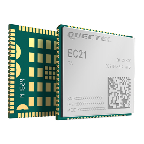
Quectel EC25 Reference Design
Lte module series
Hide thumbs
Also See for EC25:
- User manual (71 pages) ,
- Command manual (232 pages) ,
- Hardware design (43 pages)
Summary of Contents for Quectel EC25
- Page 1 EC25 Reference Design LTE Module Series Rev. EC25_Reference_Design_Rev.D Date: 2016-11-11 www.quectel.com...
- Page 2 QUECTEL OFFERS THE INFORMATION AS A SERVICE TO ITS CUSTOMERS. THE INFORMATION PROVIDED IS BASED UPON CUSTOMERS’ REQUIREMENTS. QUECTEL MAKES EVERY EFFORT TO ENSURE THE QUALITY OF THE INFORMATION IT MAKES AVAILABLE. QUECTEL DOES NOT MAKE ANY WARRANTY AS TO THE INFORMATION CONTAINED HEREIN, AND DOES NOT ACCEPT ANY LIABILITY FOR ANY INJURY, LOSS OR DAMAGE OF ANY KIND INCURRED BY USE OF OR RELIANCE UPON THE INFORMATION.
-
Page 3: About The Document
LTE Module Series EC25 Reference Design About the Document History Revision Date Author Description 2016-04-01 Winter CHEN Initial 1. Added ADC interface design in Sheet 1. 2. Added power supply for codec in Sheet 3. 3. Added note for UART Translator (Transistor... - Page 4 LTE Module Series EC25 Reference Design Contents About the Document ..........................2 Contents ..............................3 Reference Design ..........................4 1.1. Introduction ..........................4 1.2. Schematics ..........................4 EC25_Reference_Design Confidential / Released 3 / 4...
-
Page 5: Reference Design
LTE Module Series EC25 Reference Design Reference Design 1.1. Introduction This document provides the reference design for Quectel EC25 module. 1.2. Schematics The schematics illustrated in the following pages are provided for your reference only. EC25_Reference_Design Confidential / Released 4 / 4... -
Page 6: Module Interface
8. PCM_***_BT network is used for the communication with FC20 module and CODEC_PCM_*** network is used for the communication with CODEC. FC20 and CODEC can not be connected to the same PCM interface at the same time. Quectel Wireless Solutions TITLE PROJECT DRAWN BY... - Page 7 1. U201 represents customer's MCU. C201 2. EC25 can only work as a USB device and supports Full Speed and High Speed modes. To communicate with USB interface, 470nF MCU needs to support USB host or OTG function. The VBUS pins of MCU and EC25 should be powered by R203 a 5V power system for USB detection, and VBUS-CTRL is used to turn on/off VBUS power supply.
- Page 8 R316 470uF 100nF 100nF U304 R317 Note 1 R318 100K Note 2 Q303 Quectel Wireless Solutions VDD3V3=(R314/R317+1)*1.24=3.3V [1] PM_ENABLE Notes: TITLE PROJECT DTC043ZE DRAWN BY Eden LIU EC25 Reference Design 1. Recommended load current of MIC29302WU is greater than 10mA.
- Page 9 1. The decouple capacitor of USIM_VDD should be less than 1uF and must be near to USIM socket. TXS0108E 2. EC25 module provides an input pin (USIM_PRESENCE) to detect whether the USIM card exists or not. Note: It supports both low level and high level detections. For more details, please refer to It is recommended to use an IC conversion chip for UART translation.
-
Page 10: Audio Design
33pF R521 NM_0R ESD9X5.0ST5G PESD5V0S1BL PESD5V0S1BL Quectel Wireless Solutions Notes: TITLE 1. The analog output only drives earphone and headset. For larger power loads such as speakers, the design needs to incease the audio power amplifier. PROJECT DRAWN BY Reference Design... - Page 11 4. If you design the antenna circuit with passive antenna, the R603 and L603 are not needed. 5. ESD protection devices should be added to the GNSS antenna interface, and the parasitic capacitance should be less than 0.05pF. Quectel Wireless Solutions TITLE...
- Page 12 5. The differential trace impedance of SGMII must be limited to 100Ω. Quectel Wireless Solutions 6. EMI filter is reserved. If LED pins are not used, keep C714, C719, C721=470pF.
- Page 13 2. Using the 100 ohm ± 10% differential impedance with 50 ohm ± 10% single-ended impedance. Quectel Wireless Solutions 3. To minimize crosstalk, the distance between separate adjacent pairs that are on the same layer must be equal to or larger than 40 mils.
- Page 14 3. SDIO_DATA2 is a signal that affects the boot of the module, and should be kept at high level when the power supply resets. Quectel Wireless Solutions 4. The impedance of the SDIO data signal line must be controlled as 50Ω when routing.
- Page 15 1. Both USB and debug UART interfaces are reserved for software debugging. 2. USB interface also can be used to upgrade firmware. Quectel Wireless Solutions 3. Keep USB test points as close as possible to USB pins. Junction capacitance of ESD component on USB data lines might influence the signal,...


Need help?
Do you have a question about the EC25 and is the answer not in the manual?
Questions and answers