
Related Manuals for Keysight Technologies D9020DDRC


Summary of Contents for Keysight Technologies D9020DDRC
- Page 1 Keysight D9020DDRC DDR2(+LP) Compliance Test Application Methods of Implementation...
- Page 2 Notices Warranty © Keysight Technologies 2019 52.227-14 (June 1987) or DFAR 252.227-7015 (b)(2) (November 1995), as No part of this manual may be reproduced in applicable in any technical data. THE MATERIAL CONTAINED IN THIS any form or by any means (including elec- DOCUMENT IS PROVIDED "AS IS,"...
- Page 3 DDR2 —Quick Reference Table 1 DDR2 Cycles and Signals NOTE: 1 = Single Ended signal; 2 = Differential signal; 3 = 2 x Single Ended signal TEST Cycle Based on Test Definition Required Connection Type to Perform Opt. Test on Scope Read Write DQ DQS CK ADD Ctrl Data DQ DQS CK ADD Ctrl...
- Page 4 Table 1 DDR2 Cycles and Signals NOTE: 1 = Single Ended signal; 2 = Differential signal; 3 = 2 x Single Ended signal TEST Cycle Based on Test Definition Required to Perform on Scope Opt. Read Write DQ DQS CK ADD Ctrl Data DQ DQS CK ADD Ctrl Data...
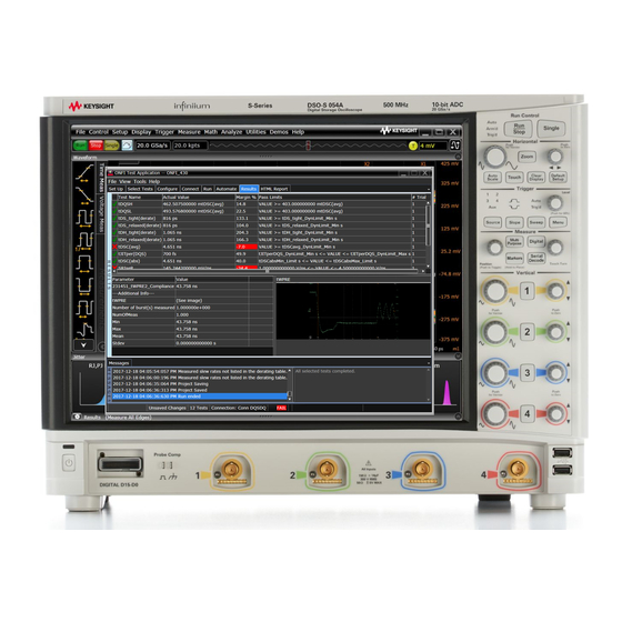
- Page 5 DDR2(+LP) Compliance Test Application — At A Glance The Keysight D9020DDRC DDR2(+LP) Compliance Test Application is a DDR2 (Double Data Rate 2) test solution that covers electrical, clock and timing parameters of the JEDEC (Joint Electronic Device Engineering Council) specifications. The software helps you in testing all the un-buffered DDR2 DUTs (devices under test) compliance, with the Keysight 9000, 90000 series, and UXR series Infiniium digital storage oscilloscope.
-
Page 6: Required Equipment And Software
Required Equipment and Software In order to run the DDR2 automated tests, you need the following equipment and software: • The minimum version of Infiniium oscilloscope software (see the D9020DDRC DDR2(+LP) test application release notes) • Use one of the following oscilloscope models: •... -
Page 7: In This Book
In This Book This manual describes the tests that are performed by the DDR2(+LP) Compliance Test Application in more detail; it contains information from (and refers to) the JESD79-2E and JESD208, and it describes how the tests are performed. • Chapter 1, “Installing the DDR2(+LP) Compliance Test Application"”... -
Page 8: See Also
20, “InfiniiMax Probing" describes the probe amplifier and probe head recommendations for DDR2(+LP) testing. See Also The DDR2(+LP) Compliance Test Application Online Help, which describes: • D9020DDRC DDR2(+LP) Automated Testing—At a Glance • Starting the D9020DDRC DDR2(+LP) Test Application • Creating or Opening a Test Project •... -
Page 9: Contact Keysight
Contact Keysight For more information on DDR2(+LP) Compliance Test Application or other Keysight Technologies’ products, applications and services, please contact your local Keysight office. The complete list is available at: www.keysight.com/find/contactus Phone or Fax United States: Korea: (tel) 800 829 4444... - Page 10 DDR2(+LP) Compliance Testing Methods of Implementation...
-
Page 11: Table Of Contents
Contents DDR2 —Quick Reference DDR2(+LP) Compliance Test Application — At A Glance Required Equipment and Software 6 In This Book See Also 8 Contact Keysight Phone or Fax 9 1 Installing the DDR2(+LP) Compliance Test Application Installing the Software Installing the License Key Using Keysight License Manager 5 Using Keysight License Manager 6 2 Preparing to Take... - Page 12 Contents Cycle to Cycle Period Jitter - tJIT(cc) - Test Method of Implementation Signals of Interest Test Definition Notes from the Specification Test References Pass Condition Measurement Algorithm Cumulative Error - tERR(n per) - Test Method of Implementation Signals of Interest Test Definition Notes from the Specification Test References Pass Condition...
- Page 13 Contents Absolute Low Pulse Width - tCL(abs) - Test Method of Implementation Signals of Interest Test Definition Notes from the Specification Test References Pass Condition Measurement Algorithm Half Period Jitter - tJIT(duty) - Test Method of Implementation Signals of Interest Test Definition Notes from the Specification Test References Pass Condition...
- Page 14 Contents VIH(AC) Test for DQS - Test Method of Implementation Signals of Interest Test Definition Notes from the Specification Test References PASS Condition Measurement Algorithm VIH(AC) Test for Address, Control - Test Method of Implementation Signals of Interest Test Definition Notes from the Specification Test References PASS Condition Measurement Algorithm...
- Page 15 Contents VIL(AC) Test for DQS - Test Method of Implementation Signals of Interest Test Definition Notes from the Specification Test References PASS Condition Measurement Algorithm VIL(AC) Test for Address, Control - Test Method of Implementation Signals of Interest Test Definition Notes from the Specification Test References PASS Condition Measurement Algorithm...
- Page 16 Contents SlewR Test for Address, Control, Clock - Test Method of Implementation Signals of Interest Test Definition Notes from the Specification Test References PASS Condition Measurement Algorithm SlewF Test for DQ, DM, DQS - Test Method of Implementation Signals of Interest Test Definition Notes from the Specification Test References PASS Condition...
- Page 17 Contents SRQseF (60ohm) - Test Method of Implementation Signals of Interest Test Definition Notes from the Specification Test References PASS Condition Measurement Algorithm VOH(AC) - Test Method of Implementation Signals of Interest Test Definition Notes from the Specification Test References PASS Condition Measurement Algorithm VOH(DC) - Test Method of Implementation...
- Page 18 Contents VIHCA(DC) - Test Method of Implementation Signals of Interest Test Definition Notes from the Specification Test References PASS Condition Measurement Algorithm VILCA(AC) - Test Method of Implementation Signals of Interest Test Definition Notes from the Specification Test References PASS Condition Measurement Algorithm VILCA(DC) - Test Method of Implementation Signals of Interest...
-
Page 19: Ddr2 -Quick Reference
Contents VILDQ(DC) - Test Method of Implementation Signals of Interest Test Definition Notes from the Specification Test References PASS Condition Measurement Algorithm 7 Single-Ended Signals AC Parameters Tests for Strobe Signals Probing for Single-Ended Signals AC parameter tests for Strobe Signals Test Procedure VSEH(AC) (strobe) - Test Method of Implementation Signals of Interest... - Page 20 Contents VIHCKE Test - Input Logic High (Clock Enable) - Test Method of Implementation Signals of Interest Test Definition Notes from the Specification Test References PASS Condition Measurement Algorithm VILCKE Test - Input Logic Low (Clock Enable) - Test Method of Implementation Signals of Interest Test Definition Notes from the Specification Test References...
-
Page 21: Ddr2(+Lp) Compliance Test Application - At A Glance
Contents VID(AC), AC Differential Input Voltage Test for Clock - Test Method of Implementation Signals of Interest Test Definition Notes from the Specification Test References PASS Condition Measurement Algorithm VIX(AC), AC Differential Input Cross Point Voltage Test for DQS -Test Method of Implementation Signals of Interest Test Definition Notes from the Specification... -
Page 22: Using Keysight License Manager
Contents VIHdiff(DC) Test for Clock - Test Method of Implementation Signals of Interest Test Definition Notes from the Specification Test References PASS Condition Measurement Algorithm VILdiff(AC) Test for DQS - Test Method of Implementation Signals of Interest Test Definition Notes from the Specification Test References PASS Condition Measurement Algorithm... - Page 23 Contents SRQdiffR (40ohm) - Test Method of Implementation Signals of Interest Test Definition Notes from the Specification Test References PASS Condition Measurement Algorithm SRQdiffF (40ohm) - Test Method of Implementation Signals of Interest Test Definition Notes from the Specification Test References PASS Condition Measurement Algorithm SRQdiffR (60ohm) - Test Method of Implementation...
- Page 24 Contents VIXCA, Clock Cross Point Voltage - Test Method of Implementation Signals of Interest Test Definition Notes from the Specification Test References PASS Condition Measurement Algorithm 13 Differential Signals Strobe Cross Point Voltage Tests Probing for Differential Signals Strobe Cross Point Voltage Tests Test Procedure VIXDQ, Strobe Cross Point Voltage - Test Method of Implementation Signals of Interest...
-
Page 25: Phone Or Fax
Contents tDVAC (Clock), Time Above VIHdiff(AC)/Below VILdiff(AC) - Test Method of Implementation Signals of Interest Test Definition Notes from the Specification Test References PASS Condition Measurement Algorithm tQHS, Data Hold Skew Factor- Test Method of Implementation Signals of Interest Test Definition Notes from the Specification Test References PASS Condition Measurement Algorithm... - Page 26 Contents tLZ(DQS), DQS Low-Impedance Time from CK/CK# - Test Method of Implementation Signals of Interest Test Definition Notes from the Specification Test References PASS Condition Measurement Algorithm tLZ(DQ), DQ Low-Impedance Time from CK/CK# - Test Method of Implementation Signals of Interest Test Definition Notes from the Specification Test References PASS Condition...
- Page 27 Contents tDQSL, DQS Input Low Pulse Width - Test Method of Implementation Signals of Interest Test Definition Notes from the Specification Test References PASS Condition Measurement Algorithm tDSS, DQS Falling Edge to CK Setup Time - Test Method of Implementation Signals of Interest Test Definition Notes from the Specification Test References...
- Page 28 Contents tRPST, Read Postamble - Test Method of Implementation Signals of Interest Test Definition Notes from the Specification Test References PASS Condition Measurement Algorithm tHZ(DQ) Test (Low Power), DQ Out HIGH Impedance Time From Clock - Test Method of Implementation Signals of Interest Test Definition Notes from the Specification Test References...
- Page 29 Contents tQSL, DQS Output Low Pulse Width - Test Method of Implementation Signals of Interest Test Definition Notes from the Specification Test References PASS Condition Measurement Algorithm tDQSS Test (Low Power), DQS Latching Transition to Associated Clock Edge - Test Method of Implementation Signals of Interest Test Definition Notes from the Specification...
- Page 30 Contents tDS(derate), Differential DQ and DM Input Setup Time with Derating Support - Test Method of Implementation Signals of Interest Test Definition Notes from the Specification Test References PASS Condition Measurement Algorithm tDH(derate), Differential DQ and DM Input Hold Time with Derating Support - Test Method of Implementation Signals of Interest Test Definition Notes from the Specification...
- Page 31 Contents tVAC (Data), Time Above VIH(AC)/Below VIL(AC) - Test Method of Implementation Signals of Interest Test Definition Notes from the Specification Test References PASS Condition Measurement Algorithm tDIPW, DQ and DM Input Pulse Width - Test Method of Implementation Signals of Interest Test Definition Notes from the Specification Test References PASS Condition...
- Page 32 Contents tIS(base) - Address and Control Input Setup Time - Test Method of Implementation Signals of Interest Test Definition Notes from the Specification Test References PASS Condition Measurement Algorithm tIH(base) - Address and Control Input Hold Time - Test Method of Implementation Signals of Interest Test Definition Notes from the Specification Test References...
- Page 33 Contents tISCKE, CKE Input Setup Time - Test Method of Implementation Signals of Interest Test Definition Notes from the Specification Test References PASS Condition Measurement Algorithm tIHCKE, CKE Input Hold Time - Test Method of Implementation Signals of Interest Test Definition Notes from the Specification Test References PASS Condition Measurement Algorithm...
- Page 34 Contents Probe Calibration Connecting the Probe for Calibration Verifying the Connection Running the Probe Calibration and Deskew Verifying the Probe Calibration 20 InfiniiMax Probing DDR2(+LP) Compliance Testing Methods of Implementation...
-
Page 35: Installing The Software / 36
Compliance Testing Methods of Implementation Installing the DDR2(+LP) Compliance Test Application Installing the Software / 36 Installing the License Key / 37 If you purchased the D9020DDRC DDR2(+LP) Compliance Test Application separately, you need to install the software and license key. - Page 36 Installing the DDR2 Compliance Test Application Installing the Software Make sure you have the minimum version of Infiniium Oscilloscope software (see D9020DDRC release notes). To ensure that you have the minimum version, select Help > About Infiniium... from the main menu.
-
Page 37: Installing The License Key
Installing the DDR2 Compliance Test Application Installing the License Key To procure a license, you require the Host ID information that is displayed in the Keysight License Manager application installed on the same machine where you wish to install the license. Using Keysight License Manager 5 To view and copy the Host ID from Keysight License Manager 5: Launch Keysight License Manager on your machine, where you wish to run the Test Application... - Page 38 Installing the DDR2 Compliance Test Application Using Keysight License Manager 6 To view and copy the Host ID from Keysight License Manager 6: Launch Keysight License Manager 6 on your machine, where you wish to run the Test Application and its features. Figure 3 Copy the Host ID, which is the first set of alphanumeric value (as highlighted in ) that...
- Page 39 Installing the DDR2 Compliance Test Application To install one of the procured licenses using Keysight License Manager 6 application, Save the license files on the machine, where you wish to run the Test Application and its features. Launch Keysight License Manager 6. From the Home tab, use one of the options to install each license file.
- Page 40 Installing the DDR2 Compliance Test Application DDR2(+LP) Compliance Testing Methods of Implementation...
-
Page 41: Preparing To Take Measurements
Keysight D9020DDRC DDR2(+LP) Compliance Test Application Compliance Testing Methods of Implementation Preparing to Take Measurements Calibrating the Oscilloscope / 26 Starting the DDR2(+LP) Compliance Test Application / 27 Before running the DDR2 automated tests, you should calibrate the oscilloscope and probe. No test fixture is required for this DDR2 application. -
Page 42: Calibrating The Oscilloscope
Preparing to Take Measurements Calibrating the Oscilloscope If you haven’t already calibrated the oscilloscope and probe, see Chapter 19, “Calibrating the Infiniium Oscilloscope and Probe. If the ambient temperature changes more than 5 degrees Celsius from the calibration temperature, NOTE internal calibration should be performed again. -
Page 43: Starting The Ddr2(+Lp) Compliance Test Application
Preparing to Take Measurements Starting the DDR2(+LP) Compliance Test Application Ensure that the RAM reliability test software is running in the computer system where the Device Under Test (DUT) is attached. This software performs tests to all unused RAM in the system by producing a repetitive burst of read-write data signals to the DDR2 memory. - Page 44 Preparing to Take Measurements If DDR2 Test does not appear in the Automated Test Apps menu, the DDR2(+LP) Compliance NOTE Test Application has not been installed (see , “Installing the Chapter 1 DDR2(+LP) Compliance Test Application). Figure 5 shows the DDR2(+LP) Compliance Test Application main window. The task flow pane, and the tabs in the main pane, show the steps you take in running the automated tests: Description Set Up...
-
Page 45: Online Help Topics
For information on using the DDR2(+LP) Compliance Test Application, see its online help (which you can access by choosing Help > Contents... from the application’s main menu). The DDR2(+LP) Compliance Test Application’s online help describes: • D9020DDRC DDR2(+LP) Automated Testing—At a Glance • Starting the D9020DDRC DDR2(+LP) Test Application •... - Page 46 Preparing to Take Measurements DDR2(+LP) Compliance Testing Methods of Implementation...
-
Page 47: Measurement Clock Tests
Keysight D9020DDRC DDR2(+LP) Compliance Test Application Compliance Testing Methods of Implementation Measurement Clock Tests Probing for Measurement Clock Tests / 32 Clock Period Jitter - tJIT(per) - Test Method of Implementation / 34 Cycle to Cycle Period Jitter - tJIT(cc) - Test Method of Implementation / 36... -
Page 48: Probing For Measurement Clock Tests
Measurement Clock Tests Probing for Measurement Clock Tests When performing the Measurement Clock tests, the DDR2(+LP) Compliance Test Application will prompt you to make the proper connections. The connections for Rising Edge and Pulse Measurement Clock tests may look similar to the following diagram. Refer to the Connection tab in DDR2 Electrical Performance Compliance application for the exact number of probe connections. - Page 49 Measurement Clock Tests Click the Select Tests tab and check the tests you want to run. Check the parent node or group to check all the available tests within the group. Figure 7 Selecting Measurement Clock Tests Follow the DDR2 Test application’s task flow to set up the configuration options, run the test, and view the test results.
-
Page 50: Clock Period Jitter - Tjit(Per) - Test Method Of Implementation
Measurement Clock Tests Clock Period Jitter - tJIT(per) - Test Method of Implementation This test is applicable to the Rising Edge Measurement and Falling Edge Measurement. The purpose of this test is to measure the difference between a measured clock period and the average clock period across multiple cycles of the clock. -
Page 51: Pass Condition
Measurement Clock Tests Pass Condition The tJIT(per) measurement value should be within the conformance limits as specified in the JEDEC specification. Measurement Algorithm Example input test signal: Frequency: 1 KHz, Number of cycles acquired: 202. This measurement measures the difference between every period inside a 200 cycle window with the average of the whole window. -
Page 52: Cycle To Cycle Period Jitter - Tjit(Cc) - Test Method Of Implementation
Measurement Clock Tests Cycle to Cycle Period Jitter - tJIT(cc) - Test Method of Implementation This test is applicable to the Rising Edge Measurement as well as Falling Edge Measurement. The purpose of this test is to measure the difference in the clock period between two consecutive clock cycles. -
Page 53: Test References
Measurement Clock Tests Test References See Specific Note 35 in the JEDEC Standard JESD79-2E, Specific Note 30 in the JESD208, and Table 103 in JESD209-2B. Pass Condition The tJIT(cc) measurement value should be within the conformance limits as specified in the JEDEC specification. -
Page 54: Cumulative Error - Terr(N Per) - Test Method Of Implementation
Measurement Clock Tests Cumulative Error - tERR(n per) - Test Method of Implementation This Cumulative Error (across “n” cycles) test is applicable to the Rising Edge Measurement as well as the Falling Edge Measurement. The purpose of this test is to measure the difference between a measured clock period and the average clock period across multiple cycles of the clock. -
Page 55: Test References
Measurement Clock Tests Table 10 LPDDR2 AC Timing Table Parameter Symbol LPDDR2 Unit 1066 466* 266* 200* Max. Frequency Clock Timing Cumulative -132 -140 -147 -162 -177 -191 -206 -221 -265 -368 (2 per), error across 2 allowed cycles Cumulative (3 per), -157 -166... -
Page 56: Measurement Algorithm
Measurement Clock Tests Measurement Algorithm Example input test signal: Frequency: 1 KHz, Number of cycles acquired: 202. tERR(2per) is similar to tJIT(per), except it makes a small 2-cycle window inside the big 200 cycle window and compares the average of the small window with the average of the big window. Calculate the average for periods 1 to 200. -
Page 57: Cumulative Error (Across 13-50 Cycles) - Terr (13-50 Per) (Low Power) - Test Method Of Implementation
Measurement Clock Tests Cumulative Error (across 13-50 cycles) - tERR (13-50 per) (Low Power) - Test Method of Im- plementation This Cumulative Error (across 13- 50 cycles) test is applicable to the Rising Edge Measurement as well as the Falling Edge Measurement. The purpose of this test is to measure the difference between a measured clock period and the average clock period across multiple cycles of the clock from 13 cycles to 50 cycles. - Page 58 Measurement Clock Tests Continue with the same procedures until the average of the last thirteen periods (188-200) is compared to the average for periods 1-200.Continue with the same procedures until the average of the last thirteen periods (188-200) is compared to the average for periods 1-200. Slide the window by one and start comparing the average of periods 2-14 and end by comparing the average of periods 189-201.
-
Page 59: Average High Pulse Width - Tch(Avg) - Test Method Of Implementation
Measurement Clock Tests Average HIGH Pulse Width - tCH(avg) - Test Method of Implementation The purpose of this test is to measure the average duty cycle of all the positive pulse widths within a window of 200 consecutive cycles. Signals of Interest Mode Supported: DDR2, LPDDR2 Signal cycle of interest: READ or WRITE Signal(s) of Interest:... -
Page 60: Measurement Algorithm
Measurement Clock Tests Measurement Algorithm Example input test signal: Frequency: 1 KHz, Number of cycles acquired: 202. Measure the sliding “window” of 200 cycles. Measure the width of the high pulses 1-200 and determine the average value for this window. By now, one measurement result is generated. -
Page 61: Absolute High Pulse Width - Tch(Abs) - Test Method Of Implementation
Measurement Clock Tests Absolute HIGH Pulse Width - tCH(abs) - Test Method of Implementation The purpose of this test is to measure the absolute duty cycle of all the positive pulse widths within a window of 200 consecutive cycles. Signals of Interest Mode Supported: LPDDR2 only Signal cycle of interest: READ or WRITE Signal(s) of Interest:... -
Page 62: Average Low Pulse Width - Tcl(Avg) - Test Method Of Implementation
Measurement Clock Tests Average Low Pulse Width - tCL(avg) - Test Method of Implementation The purpose of this test is to measure the average duty cycle of all the negative pulse widths within a window of 200 consecutive cycles. Signals of Interest Mode Supported: DDR2, LPDDR2 Signal cycle of interest: READ or WRITE Signal(s) of Interest:... -
Page 63: Measurement Algorithm
Measurement Clock Tests Measurement Algorithm Example input test signal: Frequency: 1 KHz, Number of cycles acquired: 202. Measure the sliding “window” of 200 cycles. Measure the width of the low pulses 1-200 and determine the average value for this window. By now, one measurement result is generated. -
Page 64: Absolute Low Pulse Width - Tcl(Abs) - Test Method Of Implementation
Measurement Clock Tests Absolute Low Pulse Width - tCL(abs) - Test Method of Implementation The purpose of this test is to measure the absolute duty cycle of all the negative pulse widths within a window of 202 consecutive cycles. Signals of Interest Mode Supported: LPDDR2 only Signal cycle of interest: READ or WRITE Signal(s) of Interest:... -
Page 65: Half Period Jitter - Tjit(Duty) - Test Method Of Implementation
Measurement Clock Tests Half Period Jitter - tJIT(duty) - Test Method of Implementation The Half Period Jitter tJIT(duty) can be divided into tJIT(CH) Jitter Average HIGH and tJIT(LH) Jitter Average Low. The tJIT(CH) Jitter Average HIGH Measurement measures between a positive pulse width of a cycle in the waveform, and the average positive pulse width of all cycles in a 200 consecutive cycle window. -
Page 66: Pass Condition
Measurement Clock Tests Pass Condition The tJIT(duty) measurement value should be within the conformance limits as specified in the JEDEC specification. Measurement Algorithm Example input test signal: Frequency: 1 KHz, Number of cycles acquired: 202. tJIT(CH) This measurement measures the difference between every high pulse width inside a 200 cycle window with the average of the whole window. -
Page 67: Average Clock Period - Tck(Avg) - Test Method Of Implementation
Measurement Clock Tests Average Clock Period - tCK(avg) - Test Method of Implementation This test is applicable to the Rising Edge Measurement as well as the Falling Edge Measurement. tCK(avg) is average clock period within 200 consecutive cycle window. The tCK(avg) Rising Edge Measurement measures the period from the rising edge of a cycle to the next rising edge within the waveform window. -
Page 68: Pass Condition
Measurement Clock Tests Pass Condition The tCK(avg) measurement value should be within the conformance limits as specified in the JEDEC specification. Measurement Algorithm Example input test signal: Frequency: 1 KHz, Number of cycles acquired: 202. This measurement measures a sliding “window” of 200 cycles. Calculate the average period value for periods 1-200. -
Page 69: Absolute Clock Period - Tck(Abs) - Test Method Of Implementation
Measurement Clock Tests Absolute Clock Period - tCK(abs) - Test Method of Implementation This test is applicable to the Rising Edge Measurement as well as the Falling Edge Measurement. tCK(abs) is absolute clock period within 202 consecutive cycle window. The tCK(abs) Rising Edge Measurement measures the period from the rising edge of a cycle to the next rising edge within the waveform window. - Page 70 Measurement Clock Tests DDR2(+LP) Compliance Testing Methods of Implementation...
-
Page 71: Single-Ended Signals Ac Input Parameters Tests
Keysight D9020DDRC DDR2(+LP) Compliance Test Application Compliance Testing Methods of Implementation Single-Ended Signals AC Input Parameters Tests Probing for Single-Ended Signals AC Input Parameters Tests / 56 VIH(AC) Test for DQ, DM - Test Method of Implementation / 58 VIH(AC) Test for DQS - Test Method of Implementation / 60... -
Page 72: Probing For Single-Ended Signals Ac Input Parameters Tests
Single-Ended Signals AC Input Parameters Tests Probing for Single-Ended Signals AC Input Parameters Tests When performing the Single-Ended Signals AC Input Parameters tests, the DDR2(+LP) Compliance Test Application will prompt you to make the proper connections. The connection for the Single-Ended Signals AC Input Parameters tests may look similar to the following diagram. - Page 73 Single-Ended Signals AC Input Parameters Tests Select the Speed Grade options. For the Single-Ended Signals AC Input Parameters Tests, you can select any speed grade within the selection: DDR2-400, DDR2-533, DDR2-667, DDR2-800, DDR2-1066. Type in or select the Device Identifier as well as User Description from the drop-down list. Enter your comments in the Comments text box.
-
Page 74: Vih(Ac) Test For Dq, Dm - Test Method Of Implementation
Single-Ended Signals AC Input Parameters Tests Test for DQ, DM - Test Method of Implementation IH(AC) - Maximum AC Input Logic HIGH for DQ, DM. IH(AC) The purpose of this test is to verify that voltage level of test signal at tDS (DM and DQ input setup time in JEDEC specification) before DQS midpoint is greater than the conformance lower limits of the value specified in the JEDEC specification. -
Page 75: Pass Condition
Single-Ended Signals AC Input Parameters Tests PASS Condition The voltage level at tDS (DM and DQ input setup time in JEDEC specification) before DQS midpoint for the high level voltage shall be greater than or equal to the minimum V value. -
Page 76: Vih(Ac) Test For Dqs - Test Method Of Implementation
Single-Ended Signals AC Input Parameters Tests Test for DQS - Test Method of Implementation IH(AC) - Maximum AC Input Logic HIGH for DQS. IH(AC) The purpose of this test is to verify that the high level voltage value of the test signal within a valid sampling window is greater than the conformance lower limits of the V value specified in the IH(AC) -
Page 77: Pass Condition
Single-Ended Signals AC Input Parameters Tests PASS Condition The voltage level at tDS (DM and DQ input setup time in JEDEC specification) before DQS midpoint for the high level voltage shall be greater than or equal to the minimum V value. -
Page 78: Vih(Ac) Test For Address, Control - Test Method Of Implementation
Single-Ended Signals AC Input Parameters Tests Test for Address, Control - Test Method of Implementation IH(AC) - Maximum AC Input Logic HIGH for Address, Control. IH(AC) The purpose of this test is to verify that the mode of histogram of the high level voltage value of the test signal within a valid sampling window is greater than the conformance lower limits of the V IH(AC) value specified in the JEDEC specification. -
Page 79: Pass Condition
Single-Ended Signals AC Input Parameters Tests PASS Condition The mode value for the high level voltage shall be greater than or equal to the minimum V IH(AC) value. Measurement Algorithm Sample/acquire signal data. Find all valid positive pulses. A valid positive pulse starts at V crossing at valid rising edge and end at V crossing at the following valid falling edge (See notes on threshold). -
Page 80: Vih(Dc) Test For Dq, Dm - Test Method Of Implementation
Single-Ended Signals AC Input Parameters Tests Test for DQ, DM - Test Method of Implementation IH(DC) - Minimum DC Input Logic HIGH for DQ, DM. IH(DC) The purpose of this test is to verify that the min of histogram of the high level voltage value of the test signal within a valid sampling window is within the conformance limits of the V value specified IH(DC) -
Page 81: Pass Condition
Single-Ended Signals AC Input Parameters Tests PASS Condition The minimum value of test signal from tDS before DQS midpoint to tDH after DQS midpoint for the high level voltage shall be greater than or equal to the minimum V value. IH(DC) Measurement Algorithm Acquire and split read and write burst of the acquired signal. -
Page 82: Vih(Dc) Test For Dqs - Test Method Of Implementation
Single-Ended Signals AC Input Parameters Tests Test for DQS - Test Method of Implementation IH(DC) - Minimum DC Input Logic HIGH for DQS. IH(DC) The purpose of this test is to verify that the high level voltage value of the test signal within a valid sampling window is greater than the conformance lower limits of the V value specified in the IH(DC) -
Page 83: Pass Condition
Single-Ended Signals AC Input Parameters Tests PASS Condition The high level voltage of DQS shall be greater than or equal to the minimum V value. IH(DC) Measurement Algorithm Acquire and split read and write burst of the acquired signal. (See notes on DDR read/write separation). -
Page 84: Vih(Dc) Test For Address, Control - Test Method Of Implementation
Single-Ended Signals AC Input Parameters Tests Test for Address, Control - Test Method of Implementation IH(DC) - Minimum DC Input Logic HIGH for Address, Control. IH(DC) The purpose of this test is to verify that the mode of histogram of the high level voltage value of the test signal within a valid sampling window is within the conformance limits of the V value IH(DC) -
Page 85: Pass Condition
Single-Ended Signals AC Input Parameters Tests PASS Condition The mode value for the high level voltage shall be greater than or equal to the minimum V IH(DC) value. Measurement Algorithm Sample/acquire signal data. Find all valid positive pulses. A valid positive pulse starts at V crossing at a valid rising edge and ends at V crossing at the following valid falling edge (See notes on threshold). -
Page 86: Vil(Ac) Test For Dq, Dm - Test Method Of Implementation
Single-Ended Signals AC Input Parameters Tests Test for DQ, DM - Test Method of Implementation IL(AC) - Minimum AC Input Logic Low for DQ, DM. IL(AC) The purpose of this test is to verify that voltage level of test signal at tDS (DM and DQ input setup time in JEDEC specification) before DQS midpoint is lower than the conformance maximum limits of the V value specified in the JEDEC specification. -
Page 87: Test References
Single-Ended Signals AC Input Parameters Tests Test References See Table 20 - Input AC Logic Level, in the JEDEC Standard JESD79-2E and Table 20 - Input AC Logic Level in the JESD208. PASS Condition The voltage level at tDS (DM and DQ input setup time in JEDEC specification) before DQS midpoint for the low level voltage shall be less than or equal to the maximum V value. -
Page 88: Vil(Ac) Test For Dqs - Test Method Of Implementation
Single-Ended Signals AC Input Parameters Tests Test for DQS - Test Method of Implementation IL(AC) - Minimum AC Input Logic Low for DQS. IL(AC) The purpose of this test is to verify that the low level voltage value of the test signal within a valid sampling window is lower than the conformance maximum limits of the V value specified in the IL(AC) -
Page 89: Test References
Single-Ended Signals AC Input Parameters Tests Test References See Table 20 - Input AC Logic Level, in the JEDEC Standard JESD79-2E and Table 20 - Input AC Logic Level in the JESD208. PASS Condition The low level voltage of DQS shall be less than or equal to the maximum V value. -
Page 90: Vil(Ac) Test For Address, Control - Test Method Of Implementation
Single-Ended Signals AC Input Parameters Tests Test for Address, Control - Test Method of Implementation IL(AC) - Minimum AC Input Logic Low Address, Control. IL(AC) The purpose of this test is to verify that the mode low level voltage value of the histogram for the test signal is lower than the conformance maximum limits of the V value specified in the JEDEC IL(AC) -
Page 91: Test References
Single-Ended Signals AC Input Parameters Tests Test References See Table 20 - Input AC Logic Level, in the JEDEC Standard JESD79-2E and Table 20 - Input AC Logic Level in the JESD208. PASS Condition The mode value for the histogram for the low level voltage shall be less than or equal to the maximum V value. -
Page 92: Vil(Dc) Test For Dq, Dm - Test Method Of Implementation
Single-Ended Signals AC Input Parameters Tests Test for DQ, DM - Test Method of Implementation IL(DC) - Maximum DC Input Logic Low for DQ, DM. IL(DC) The purpose of this test is to verify that the max of histogram of the low level voltage value of the test signal within a valid sampling window is within the conformance limits of the V value specified in IL(DC) -
Page 93: Pass Condition
Single-Ended Signals AC Input Parameters Tests PASS Condition The maximum value of test signal from tDS before DQS midpoint to tDH after DQS midpoint for the low level voltage shall be less than or equal to the maximum V value. IL(DC) Measurement Algorithm Acquire and split read and write burst of the acquired signal. -
Page 94: Vil(Dc) Test For Dqs - Test Method Of Implementation
Single-Ended Signals AC Input Parameters Tests Test for DQS - Test Method of Implementation IL(DC) - Maximum DC Input Logic Low for DQS. IL(DC) The purpose of this test is to verify that the low level voltage value of the test signal within a valid sampling window is lower than the conformance maximum limits of the V value specified in the IL(DC) -
Page 95: Pass Condition
Single-Ended Signals AC Input Parameters Tests PASS Condition The low level voltage of DQS shall be less than or equal to the maximum V value. IL(DC) Measurement Algorithm Acquire and split read and write burst of the acquired signal. (See notes on DDR read/write separation). -
Page 96: Vil(Dc) Test For Address, Control - Test Method Of Implementation
Single-Ended Signals AC Input Parameters Tests Test for Address, Control - Test Method of Implementation IL(DC) - Maximum DC Input Logic Low for Address, Control. IL(DC) The purpose of this test is to verify that the mode of histogram of the low level voltage value of the test signal within a valid sampling window is within the conformance limits of the V value IL(DC) -
Page 97: Pass Condition
Single-Ended Signals AC Input Parameters Tests PASS Condition The mode value for the histogram for the low level voltage shall be less than or equal to the maximum V value. IL(DC) Measurement Algorithm Sample/acquire signal data. Find all valid negative pulses. A valid negative pulse starts at V crossing at valid falling edge and end at V crossing at the following rising valid edge (See notes on threshold). -
Page 98: Slewr Test For Dq, Dm, Dqs - Test Method Of Implementation
Single-Ended Signals AC Input Parameters Tests Slew Test for DQ, DM, DQS - Test Method of Implementation Slew - Input Signal Minimum Slew Rate (Rising) for DQ, DM, DQS. The purpose of this test is to verify that the rising slew rate value of the test signal is greater than or equal to the conformance limit of the input SLEW value specified in the JEDEC specification. -
Page 99: Test References
Single-Ended Signals AC Input Parameters Tests Test References See Table 21 - AC Input Test Conditions in the JEDEC Standard JESD79-2E and Table 21 - AC Input Test Conditions in the JESD208. PASS Condition The calculated Rising Slew value of the test signal should be greater than or equal to the SLEW value. -
Page 100: Slewr Test For Address, Control, Clock - Test Method Of Implementation
Single-Ended Signals AC Input Parameters Tests Slew Test for Address, Control, Clock - Test Method of Implementation Slew - Input Signal Minimum Slew Rate (Rising) for Address, Control, Clock. The purpose of this test is to verify that the rising slew rate value of the test signal is greater than or equal to the conformance limit of the input SLEW value specified in the JEDEC specification. -
Page 101: Test References
Single-Ended Signals AC Input Parameters Tests Test References See Table 21 - AC Input Test Conditions in the JEDEC Standard JESD79-2E and Table 21 - AC Input Test Conditions in the JESD208. PASS Condition The calculated Rising Slew value of the test signal should be greater than or equal to the SLEW value. -
Page 102: Slewf Test For Dq, Dm, Dqs - Test Method Of Implementation
Single-Ended Signals AC Input Parameters Tests Slew Test for DQ, DM, DQS - Test Method of Implementation Slew - Input Signal Minimum Slew Rate (Falling) for DQ, DM, DQS. The purpose of this test is to verify that the falling slew rate value of the test signal is greater than or equal to the conformance limit of the input SLEW value specified in the JEDEC specification. -
Page 103: Test References
Single-Ended Signals AC Input Parameters Tests Test References See Table 21 - AC Input Test Conditions in the JEDEC Standard JESD79-2E and Table 21 - AC Input Test Conditions in the JESD208. PASS Condition The calculated Falling Slew value for the test signal should be greater than or equal to the SLEW value. -
Page 104: Slewf Test For Address, Control, Clock - Test Method Of Implementation
Single-Ended Signals AC Input Parameters Tests Slew Test for Address, Control, Clock - Test Method of Implementation Slew - Input Signal Minimum Slew Rate (Falling) for Address, Control, Clock. The purpose of this test is to verify that the falling slew rate value of the test signal is greater than or equal to the conformance limit of the input SLEW value specified in the JEDEC specification. -
Page 105: Test References
Single-Ended Signals AC Input Parameters Tests Test References See Table 21 - AC Input Test Conditions in the JEDEC Standard JESD79-2E and Table 21 - AC Input Test Conditions in the JESD208. PASS Condition The calculated Falling Slew value for the test signal should be greater than or equal to the SLEW value. -
Page 106: Srqser (40Ohm) - Test Method Of Implementation
Single-Ended Signals AC Input Parameters Tests SRQseR (40ohm) - Test Method of Implementation AC Output Parameter Tests can be divided into eight sub tests: • SRQseR(40ohm) test • SRQseF(40ohm) test • SRQseR(60ohm) test • SRQseF(60ohm) test • test OH(AC) • test OH(DC) •... -
Page 107: Measurement Algorithm
Single-Ended Signals AC Input Parameters Tests Measurement Algorithm Acquire and split read and write bursts of the acquired signal. Take the first valid READ burst found. Find all valid signal rising edges in this burst. A valid signal rising edge starts at the V OL(AC) crossing and ends at the following V crossing. -
Page 108: Srqsef (40Ohm) - Test Method Of Implementation
Single-Ended Signals AC Input Parameters Tests SRQseF (40ohm) - Test Method of Implementation SRQseF (40ohm) - Single-ended Output Falling Slew Rate (40ohms). The purpose of this test is to verify that the single-ended falling slew rate value of the test signal must be within the conformance limit of the SRQse value as specified in the JEDEC specification. -
Page 109: Srqser (60Ohm) - Test Method Of Implementation
Single-Ended Signals AC Input Parameters Tests SRQseR (60ohm) - Test Method of Implementation SRQseR (60ohm) - Single-ended Output Rising Slew Rate (60ohms). The purpose of this test is to verify that the single-ended rising slew rate value of the test signal must be within the conformance limit of the SRQse value as specified in the JEDEC specification. -
Page 110: Srqsef (60Ohm) - Test Method Of Implementation
Single-Ended Signals AC Input Parameters Tests SRQseF (60ohm) - Test Method of Implementation SRQseF (60ohm) - Single-ended Output Falling Slew Rate (60ohms). The purpose of this test is to verify that the single-ended falling slew rate value of the test signal must be within the conformance limit of the SRQse value as specified in the JEDEC specification. -
Page 111: Voh(Ac) - Test Method Of Implementation
Single-Ended Signals AC Input Parameters Tests - Test Method of Implementation OH(AC) - Single-ended AC Output Logic High Voltage. OH(AC) The purpose of this test is to verify that the high level voltage value of the test signal within a valid sampling window must be within the conformance limit of the V value as specified in the OH(AC) -
Page 112: Voh(Dc) - Test Method Of Implementation
Single-Ended Signals AC Input Parameters Tests - Test Method of Implementation OH(DC) - Single-ended DC Output Logic High Voltage. OH(DC) The purpose of this test is to verify that the high level voltage value of the test signal within a valid sampling window must be within the conformance limit of the V value as specified in the OH(DC) -
Page 113: Vol(Ac) - Test Method Of Implementation
Single-Ended Signals AC Input Parameters Tests - Test Method of Implementation OL(AC) - Single-ended AC Output Logic Low Voltage. OL(AC) The purpose of this test is to verify that the low level voltage value of the test signal within a valid sampling window must be within the conformance limit of the V value as specified in the JEDEC OL(AC) -
Page 114: Vol(Dc) - Test Method Of Implementation
Single-Ended Signals AC Input Parameters Tests - Test Method of Implementation OL(DC) - Single-ended DC Output Logic High Voltage. OH(DC) The purpose of this test is to verify that the low level voltage value of the test signal within a valid sampling window must be within the conformance limit of the V value as specified in the OL(DC) - Page 115 Keysight D9020DDRC DDR2(+LP) Compliance Test Application Compliance Testing Methods of Implementation Single-Ended Signals V (Address, Control) Tests Probing for Single-Ended Signals VIH/VIL (Address, Control) Tests / 100 VIHCA(AC) - Test Method of Implementation / 102 VIHCA(DC) - Test Method of Implementation / 104...
-
Page 116: (Address, Control) Tests
Single-Ended Signals VIH/VIL (Address, Control) Tests Probing for Single-Ended Signals V (Address, Control) Tests When performing the Single-Ended Signals V (Address, Control) tests, the DDR2(+LP) Compliance Test Application will prompt you to make the proper connections. The connection for the Single-Ended Signals V (Address, Control) tests may look similar to the following diagram. - Page 117 Single-Ended Signals VIH/VIL (Address, Control) Tests In the DDR2(+LP) Test application, click the Set Up tab. Select the Speed Grade options. For the Single-Ended Signals V (Address, Control) tests, you can select any LPDDR2 speed grade within the selection. To see the LPDDR2 Speed Grades, check the Low Power box.
-
Page 118: Vihca(Ac) - Test Method Of Implementation
Single-Ended Signals VIH/VIL (Address, Control) Tests - Test Method of Implementation IHCA(AC) Input Logic HIGH (Address, Control) test can be divided into two subtests: • test IHCA(AC) • test IHCA(DC) - AC Input Logic HIGH (Address, Control). IHCA(AC) The purpose of this test is to verify that the histogram mode high level voltage value of the test signal within a valid sampling window is greater than the conformance lower limits of the V value IHCA(AC) -
Page 119: Measurement Algorithm
Single-Ended Signals VIH/VIL (Address, Control) Tests Measurement Algorithm Sample/acquire signal data. Find all valid positive pulses. A valid positive pulse starts at V crossing at valid rising edge and end at V crossing at the following valid falling edge (See notes on threshold). Zoom in on the first valid positive pulse and perform V measurement. -
Page 120: Vihca(Dc) - Test Method Of Implementation
Single-Ended Signals VIH/VIL (Address, Control) Tests - Test Method of Implementation IHCA(DC) - DC Input Logic HIGH (Address, Control). IHCA(DC) The purpose of this test is to verify that the histogram mode high level voltage value of the test signal within a valid sampling window is greater than the conformance lower limits of the V value IHCA(DC) -
Page 121: Vilca(Ac) - Test Method Of Implementation
Single-Ended Signals VIH/VIL (Address, Control) Tests - Test Method of Implementation ILCA(AC) Input Logic Low (Address, Control) test can be divided into two subtests: • test ILCA(AC) • test ILCA(DC) - AC Input Logic Low (Address, Control). ILCA(AC) The purpose of this test is to verify that the histogram mode low level voltage value of the test signal within a valid sampling window is lower than the conformance lower limits of the V value ILCA(AC) -
Page 122: Vilca(Dc) - Test Method Of Implementation
Single-Ended Signals VIH/VIL (Address, Control) Tests - Test Method of Implementation ILCA(DC) - DC Input Logic Low (Address, Control). ILCA(DC) The purpose of this test is to verify that the histogram mode low level voltage value of the test signal within a valid sampling window is lower than the conformance lower limits of the V value ILCA(DC) - Page 123 Keysight D9020DDRC DDR2(+LP) Compliance Test Application Compliance Testing Methods of Implementation Single-Ended Signals V (Data, Mask) Tests Probing for Single-Ended Signals VIH/VIL (Data, Mask) Tests / 108 VIHDQ(AC) - Test Method of Implementation / 110 VIHDQ(DC) - Test Method of Implementation / 112...
-
Page 124: Single-Ended Signals Vih/Vil
Single-Ended Signals VIH/VIL (Data, Mask) Tests Probing for Single-Ended Signals V (Data, Mask) Tests When performing the Single-Ended Signals V (Data, Mask) tests, the DDR2(+LP) Compliance Test Application will prompt you to make the proper connections. The connection for the Single-Ended Signals V (Data, Mask) tests may look similar to the following diagram. - Page 125 Single-Ended Signals VIH/VIL (Data, Mask) Tests In the DDR2(+LP) Test application, click the Set Up tab. Select the Speed Grade options. For the Single-Ended Signals V (Data, Mask) tests, you can select any LPDDR2 speed grade within the selection. To see the LPDDR2 Speed Grades, check the Low Power box.
-
Page 126: Vihdq(Ac) - Test Method Of Implementation
Single-Ended Signals VIH/VIL (Data, Mask) Tests - Test Method of Implementation IHDQ(AC) Input Logic HIGH (Data, Mask) test can be divided into two subtests: • test IHDQ(AC) • test IHDQ(DC) - AC Input Logic HIGH (Data, Mask). IHDQ(AC) The purpose of this test is to verify that the voltage level of the test signal at tDS (DM and DQ input setup time in JEDEC specification) before the DQS midpoint is greater than the conformance lower limits of the V value specified in the JEDEC specification. -
Page 127: Measurement Algorithm
Single-Ended Signals VIH/VIL (Data, Mask) Tests Measurement Algorithm Acquire and split read and write bursts of the acquired signal. Take the first valid WRITE burst found. Find all valid rising DQ crossings that cross V in the burst. IH(AC) For all DQ crossings found, locate all the following DQS crossings that cross 0V. Calculate the time where the test result is taken. -
Page 128: Vihdq(Dc) - Test Method Of Implementation
Single-Ended Signals VIH/VIL (Data, Mask) Tests - Test Method of Implementation IHDQ(DC) - DC Input Logic HIGH (Data, Mask). IHDQ(DC) The purpose of this test is to verify that the histogram min high level voltage value of the test signal within a valid sampling window is within the conformance limits of the V value specified in IHDQ(DC) -
Page 129: Measurement Algorithm
Single-Ended Signals VIH/VIL (Data, Mask) Tests Measurement Algorithm Acquire and split read and write bursts of the acquired signal. Take the first valid WRITE burst found. Find all valid rising DQ crossings that cross V in the burst. IH(AC) For all DQ crossings found, locate all the following DQS crossings that cross midpoint. (0V is for differential DQS and V is for single ended DQS.) Set up histogram function settings. -
Page 130: Vildq(Ac) - Test Method Of Implementation
Single-Ended Signals VIH/VIL (Data, Mask) Tests - Test Method of Implementation ILDQ(AC) Input Logic Low (Data, Mask) test can be divided into two subtests: • test ILDQ(AC) • test ILDQ(DC) - AC Input Logic Low (Data, Mask). ILDQ(AC) The purpose of this test is to verify that the voltage level of the test signal at tDS (DM and DQ input setup time in JEDEC specification) before the DQS midpoint is lower than the conformance lower limits of the V value specified in the JEDEC specification. -
Page 131: Measurement Algorithm
Single-Ended Signals VIH/VIL (Data, Mask) Tests Measurement Algorithm Acquire and split read and write bursts of the acquired signal. Take the first valid WRITE burst found. Find all valid falling DQ crossings that cross V in the burst. IL(AC) For all DQ crossings found, locate all the following DQS crossings that cross midpoint. (0V is for differential DQS and V is for single ended DQS.). -
Page 132: Vildq(Dc) - Test Method Of Implementation
Single-Ended Signals VIH/VIL (Data, Mask) Tests - Test Method of Implementation ILDQ(DC) - DC Input Logic Low (Data, Mask). ILDQ(DC) The purpose of this test is to verify that the histogram max low level voltage value of the test signal within a valid sampling window is within the conformance limits of the V value specified in the ILDQ(DC) -
Page 133: Measurement Algorithm
Single-Ended Signals VIH/VIL (Data, Mask) Tests Measurement Algorithm Acquire and split read and write bursts of the acquired signal. Take the first valid WRITE burst found. Find all valid rising DQ crossings that cross V in the burst. IL(AC) For all DQ crossings found, locate all the following DQS crossings that cross midpoint. (0V is for differential DQS and V is for single ended DQS.) Set up histogram function settings. - Page 134 Single-Ended Signals VIH/VIL (Data, Mask) Tests DDR2(+LP) Compliance Testing Methods of Implementation...
-
Page 135: Single-Ended Signals Ac Parameters Tests For Strobe Signals
Keysight D9020DDRC DDR2(+LP) Compliance Test Application Compliance Testing Methods of Implementation Single-Ended Signals AC Parameters Tests for Strobe Signals Probing for Single-Ended Signals AC parameter tests for Strobe Signals / 120 VSEH(AC) (strobe) - Test Method of Implementation / 122... -
Page 136: Probing For Single-Ended Signals Ac Parameter Tests For Strobe Signals
Single-Ended Signals AC parameter tests for Strobe Signals Probing for Single-Ended Signals AC parameter tests for Strobe Signals When performing the Single-Ended Signals AC parameter tests for Strobe Signals, the DDR2(+LP) Compliance Test Application will prompt you to make the proper connections. The connection for the Single-Ended Signals AC parameter tests for Strobe Signals may look similar to the following diagram. - Page 137 Single-Ended Signals AC parameter tests for Strobe Signals In the DDR2(+LP) Test application, click the Set Up tab. Select the Speed Grade options. For the Single-Ended Signals AC parameter tests for Strobe Signals, you can select any LPDDR2 speed grade within the selection. To see the LPDDR2 Speed Grades, check the Low Power box.
-
Page 138: Vseh(Ac) (Strobe) - Test Method Of Implementation
Single-Ended Signals AC parameter tests for Strobe Signals (strobe) - Test Method of Implementation SEH(AC) Single-ended Signal Tests for Strobe Tests can be divided into two subtests: • test SEH(AC) • test SEL(AC) - Single- ended High Level Voltage. SEH(AC) The purpose of this test is to verify that the maximum high pulse voltage must be within the conformance limit of the V value as specified in the JEDEC specification. -
Page 139: Measurement Algorithm
Single-Ended Signals AC parameter tests for Strobe Signals Measurement Algorithm Acquire and split read and write bursts of the acquired signal. Take the first valid WRITE burst found. Find all valid strobe positive pulses in this burst. A valid strobe positive pulse starts at the V crossing on a valid strobe rising edge and ends at the V crossing on the following valid strobe falling edge. -
Page 140: Vsel(Ac) (Strobe) - Test Method Of Implementation
Single-Ended Signals AC parameter tests for Strobe Signals (strobe) - Test Method of Implementation SEL(AC) - Single- ended Low Level Voltage. SEL(AC) The purpose of this test is to verify that the minimum low pulse voltage must be within the conformance limit of the V value as specified in the JEDEC specification. -
Page 141: Single-Ended Signals Ac Parameters Tests For Clock
Keysight D9020DDRC DDR2(+LP) Compliance Test Application Compliance Testing Methods of Implementation Single-Ended Signals AC Parameters Tests for Clock Probing for Single-Ended Signals AC parameter tests for Clock / 126 VSEH(AC) (clock) - Test Method of Implementation / 128 VSEL(AC) (clock) - Test Method of Implementation / 130... -
Page 142: Probing For Single-Ended Signals Ac Parameter Tests For Clock
Single-Ended Signals AC parameter tests for Clocks Probing for Single-Ended Signals AC parameter tests for Clock When performing the Single-Ended Signals AC parameter tests for Clocks, the DDR2(+LP) Compliance Test Application will prompt you to make the proper connections. The connection for the Single-Ended Signals AC parameter tests for Clocks may look similar to the following diagram. - Page 143 Single-Ended Signals AC parameter tests for Clocks In the DDR2(+LP) Test application, click the Set Up tab. Select the Speed Grade options. For the Single-Ended Signals AC parameter tests for Clocks, you can select any LPDDR2 speed grade within the selection. To see the LPDDR2 Speed Grades, check the Low Power box.
-
Page 144: Vseh(Ac) (Clock) - Test Method Of Implementation
Single-Ended Signals AC parameter tests for Clocks (clock) - Test Method of Implementation SEH(AC) Single-ended Signal Tests for Clock Tests can be divided into two subtests: • test SEH(AC) • test SEL(AC) - Single- ended High Level Voltage. SEH(AC) The purpose of this test is to verify that the maximum high pulse voltage must be within the conformance limit of the V value as specified in the JEDEC specification. -
Page 145: Measurement Algorithm
Single-Ended Signals AC parameter tests for Clocks Measurement Algorithm Pre-condition the oscilloscope. Trigger on a rising edge of the clock signal under test. Find all valid Clock positive pulses in the entire waveform. A valid Clock positive pulse starts at the V crossing on a valid Clock rising edge and ends at the V crossing on the following... -
Page 146: Vsel(Ac) (Clock) - Test Method Of Implementation
Single-Ended Signals AC parameter tests for Clocks (clock) - Test Method of Implementation SEL(AC) - Single- ended Low Level Voltage. SEL(AC) The purpose of this test is to verify that the minimum low pulse voltage must be within the conformance limit of the V value as specified in the JEDEC specification. -
Page 147: Vihcke Test - Input Logic High (Clock Enable) - Test Method Of Implementation
Single-Ended Signals AC parameter tests for Clocks Test - Input Logic High (Clock Enable) - Test Method of Implementation IHCKE The purpose of this test is to verify that the mode of histogram of the high level voltage value of the test signal within a valid sampling window is greater than the conformance lower limits of the V IHCKE value specified in the JEDEC specification. -
Page 148: Vilcke Test - Input Logic Low (Clock Enable) - Test Method Of Implementation
Single-Ended Signals AC parameter tests for Clocks Test - Input Logic Low (Clock Enable) - Test Method of Implementation ILCKE The purpose of this test is to verify that the mode of histogram of the low level voltage value of the test signal within a valid sampling window is lower than the conformance maximum limits of the value specified in the JEDEC specification. -
Page 149: Single-Ended Signals Overshoot/Undershoot Tests
Keysight D9020DDRC DDR2(+LP) Compliance Test Application Compliance Testing Methods of Implementation Single-Ended Signals Overshoot/Undershoot Tests Probing for Overshoot/Undershoot Tests / 134 AC Overshoot Test Method of Implementation / 136 AC Undershoot Test Method of Implementation / 139 This section provides the Methods of Implementation (MOIs) for Single-Ended Signals... -
Page 150: Probing For Overshoot/Undershoot Tests
Single-Ended Signals Overshoot/Undershoot Tests Probing for Overshoot/Undershoot Tests When performing the Single-Ended Signals Overshoot/Undershoot tests, the DDR2(+LP) Compliance Test Application will prompt you to make the proper connections as shown in the following diagram. Refer to the Connection tab in DDR2(+LP) Electrical Performance Compliance application for the exact number of probe connections. - Page 151 Single-Ended Signals Overshoot/Undershoot Tests Type in or select the Device Identifier as well as User Description from the drop-down list. Enter your comments in the Comments text box. Click the Select Tests tab and check the tests you want to run. Check the parent node or group to check all the available tests within the group.
-
Page 152: Ac Overshoot Test Method Of Implementation
Single-Ended Signals Overshoot/Undershoot Tests AC Overshoot Test Method of Implementation The Overshoot test can be divided into two sub-tests: Overshoot amplitude and overshoot area. The purpose of this test is to verify that the overshoot value of the test signal within a user-specific region is lower than or equal to the conformance limit of the maximum peak amplitude allowed for overshoot test as specified in the JEDEC specification. - Page 153 Single-Ended Signals Overshoot/Undershoot Tests Table 83 AC Overshoot Specification for Address and Control Pins (DDR2-1066) A0-A15, BA0-BA2, CS, RAS, CAS, WE, CKE, ODT Parameter Specification DDR2-1066 Maximum peak amplitude allowed for overshoot area 0.5(0.9) Maximum overshoot area above V 0.5 V-ns Table 84 AC Overshoot Specification for Clock, Data, Strobe and Mask Pins (DDR2-1066) DQ, (U/L/R)DQS, (U/L/R)DQS, DM, CK, CK...
-
Page 154: Test References
Single-Ended Signals Overshoot/Undershoot Tests Test References See Table 24 - AC Overshoot/Undershoot Specification for Address and Control Pins and Table 25 - AC Overshoot/Undershoot Specification for Clock, Data, Strobe and Mask Pins in the JEDEC Standard JESD79-2E. Also See Table 24 - AC Overshoot/Undershoot Specification for Address and Control Pins and Table 25 - AC Overshoot/Undershoot Specification for Clock, Data, Strobe and Mask Pins in the JESD208. -
Page 155: Ac Undershoot Test Method Of Implementation
Single-Ended Signals Overshoot/Undershoot Tests AC Undershoot Test Method of Implementation The Undershoot Test can be divided into two sub-tests: Undershoot amplitude and Undershoot area. The purpose of this test is to verify that the undershoot value of the test signal within a user-specific region is lower than or equal to the conformance limit of the maximum peak amplitude allowed for undershoot test as specified in the JEDEC specification. - Page 156 Single-Ended Signals Overshoot/Undershoot Tests Table 88 AC Undershoot Specification for Address and Control Pins (DDR2-1066) A0-A15, BA0-BA2, CS, RAS, CAS, WE, CKE, ODT Parameter Specification DDR2-1066 Maximum peak amplitude allowed for undershoot area 0.5(0.9) Maximum undershoot area below V 0.5 V-ns Table 89 AC Undershoot Specification for Clock, Data, Strobe and Mask Pins (DDR2-1066) DQ, (U/L/R)DQS, (U/L/R)DQS, DM, CK, CK...
-
Page 157: Test References
Single-Ended Signals Overshoot/Undershoot Tests Test References See Table 24 - AC Overshoot/Undershoot Specification for Address and Control Pins and Table 25 - AC Overshoot/Undershoot Specification for Clock, Data, Strobe and Mask Pins, in the JEDEC Standard JESD79-2E. Also See Table 24 - AC Overshoot/Undershoot Specification for Address and Control Pins and Table 25 - AC Overshoot/Undershoot Specification for Clock, Data, Strobe and Mask Pins in the JESD208. - Page 158 Single-Ended Signals Overshoot/Undershoot Tests DDR2(+LP) Compliance Testing Methods of Implementation...
-
Page 159: Differential Signals Ac Input Parameters Tests
Keysight D9020DDRC DDR2(+LP) Compliance Test Application Compliance Testing Methods of Implementation 10 Differential Signals AC Input Parameters Tests Probing for Differential Signals AC Input Parameters Tests / 144 VID(AC), AC Differential Input Voltage Test for DQS - Test Method of Implementation / 146... -
Page 160: Probing For Differential Signals Ac Input Parameters Tests
Differential Signals AC Input Parameters Tests Probing for Differential Signals AC Input Parameters Tests When performing the Differential Signals AC Input Parameters tests, the DDR2(+LP) Compliance Test Application will prompt you to make the proper connections. The connection for the Differential Signals AC Input Parameters tests may look similar to the following diagram. - Page 161 Differential Signals AC Input Parameters Tests Select the Speed Grade options. For Differential Signals AC Input Parameters Tests that support DDR2, you can select any speed grade within the selection. To select a LPDDR2 Speed Grade (for tests that support LPDDR2), check the Low Power box. Type in or select the Device Identifier as well as User Description from the drop-down list.
-
Page 162: Vid(Ac), Ac Differential Input Voltage Test For Dqs - Test Method Of Implementation
Differential Signals AC Input Parameters Tests , AC Differential Input Voltage Test for DQS - Test Method of Implementation ID(AC) The purpose of this test is to verify that magnitude differences between the input differential signal pairs value of the test signals is within the conformance limits of the V as specified in the JEDEC ID(AC) specification. -
Page 163: Test References
Differential Signals AC Input Parameters Tests Test References See Table 22 - Differential Input AC Logic Level in the JEDEC Standard JESD79-2E and Table 22 - Differential Input AC Logic Level in the JESD208. PASS Condition The calculated magnitude of the differential voltage of the test signals pair should be within the conformance limits of the V value. -
Page 164: Vid(Ac), Ac Differential Input Voltage Test For Clock - Test Method Of Implementation
Differential Signals AC Input Parameters Tests , AC Differential Input Voltage Test for Clock - Test Method of Implementation ID(AC) The purpose of this test is to verify that magnitude differences between the input differential signal pairs value of the test signals is within the conformance limits of the V as specified in the JEDEC ID(AC) specification. -
Page 165: Test References
Differential Signals AC Input Parameters Tests Test References See Table 22 - Differential Input AC Logic Level in the JEDEC Standard JESD79-2E and Table 22 - Differential Input AC Logic Level in the JESD208. PASS Condition The calculated magnitude of the differential voltage of the test signals pair should be within the conformance limits of the V value. -
Page 166: Vix(Ac), Ac Differential Input Cross Point Voltage Test For Dqs -Test Method Of Implementation
Differential Signals AC Input Parameters Tests , AC Differential Input Cross Point Voltage Test for DQS -Test Method of Implementation IX(AC) The purpose of this test is to verify the crossing point voltage value of the input differential test signals pair is within the conformance limits of the V as specified in the JEDEC specification. -
Page 167: Test References
Differential Signals AC Input Parameters Tests Test References See Table 22 - Differential Input AC Logic Level in the JEDEC Standard JESD79-2E and Table 22 - Differential Input AC Logic Level in the JESD208. PASS Condition The measured crossing point value for the differential test signals pair should be within the conformance limits of V value. -
Page 168: Vix(Ac), Ac Differential Input Cross Point Voltage Test For Clock -Test Method Of Implementation
Differential Signals AC Input Parameters Tests , AC Differential Input Cross Point Voltage Test for Clock -Test Method of Implementa- IX(AC) tion The purpose of this test is to verify the crossing point voltage value of the input differential test signals pair is within the conformance limits of the V as specified in the JEDEC specification. -
Page 169: Test References
Differential Signals AC Input Parameters Tests Test References See Table 22 - Differential Input AC Logic Level in the JEDEC Standard JESD79-2E and Table 22 - Differential Input AC Logic Level in the JESD208. PASS Condition The measured crossing point value for the differential test signals pair should be within the conformance limits of V value. -
Page 170: Vihdiff(Ac) Test For Dqs - Test Method Of Implementation
Differential Signals AC Input Parameters Tests Test for DQS - Test Method of Implementation IHdiff(AC) - Differential AC Input Logic High Voltage Test for DQS. IHdiff(AC) The purpose of this test is to verify that the high level voltage value of the test signal within a valid sampling window must be within the conformance limit of the V value as specified in the IHdiff(AC) -
Page 171: Measurement Algorithm
Differential Signals AC Input Parameters Tests Measurement Algorithm Acquire and split read and write bursts of the acquired signal. (See notes on DDR read/write separation). Take the first valid WRITE burst found. Find all valid Strobe positive pulses in the burst. A valid Strobe positive pulse starts at 0 Volt crossing at valid Strobe rising edge (see notes on threshold) and ends at the 0V crossing on the following valid Strobe falling edge (see notes on threshold). -
Page 172: Vihdiff(Ac) Test For Clock - Test Method Of Implementation
Differential Signals AC Input Parameters Tests Test for Clock - Test Method of Implementation IHdiff(AC) - Differential AC Input Logic High Voltage Test for Clock. IHdiff(AC) The purpose of this test is to verify that the high level voltage value of the test signal within a valid sampling window must be within the conformance limit of the V value as specified in the IHdiff(AC) -
Page 173: Measurement Algorithm
Differential Signals AC Input Parameters Tests Measurement Algorithm Pre-condition the oscilloscope. Trigger on a rising edge of the clock signal under test. Find all valid Clock positive pulses in the triggered waveform. A valid Clock positive pulse starts at the 0V crossing on a valid Clock rising edge (see notes on threshold) and ends at the 0V crossing on the following valid Clock falling edge (see notes on threshold). -
Page 174: Vihdiff(Dc) Test For Dqs - Test Method Of Implementation
Differential Signals AC Input Parameters Tests Test for DQS - Test Method of Implementation IHdiff(DC) - Differential DC Input Logic High Voltage Test for DQS. IHdiff(DC) The purpose of this test is to verify that the high level voltage value of the test signal within a valid sampling window must be within the conformance limit of the V value as specified in the IHdiff(DC) -
Page 175: Measurement Algorithm
Differential Signals AC Input Parameters Tests Measurement Algorithm Acquire and split read and write bursts of the acquired signal. (See notes on DDR read/write separation). Take the first valid WRITE burst found. Find all valid Strobe positive pulses in the burst. A valid Strobe positive pulse starts at the 0V crossing on a valid Strobe rising edge (see notes on threshold) and ends at the 0V crossing on the following valid Strobe falling edge (see notes on threshold). -
Page 176: Vihdiff(Dc) Test For Clock - Test Method Of Implementation
Differential Signals AC Input Parameters Tests Test for Clock - Test Method of Implementation IHdiff(DC) - Differential DC Input Logic High Voltage Test for Clock. IHdiff(DC) The purpose of this test is to verify that the high level voltage value of the test signal within a valid sampling window must be within the conformance limit of the V value as specified in the IHdiff(DC) -
Page 177: Measurement Algorithm
Differential Signals AC Input Parameters Tests Measurement Algorithm Pre-condition the oscilloscope. Trigger on a rising edge of the clock signal under test. Find all valid Clock positive pulses in the triggered waveform. A valid Clock positive pulse starts at the 0V crossing on a valid Clock rising edge (see notes on threshold) and ends at the 0V crossing on the following valid Clock falling edge (see notes on threshold). -
Page 178: Vildiff(Ac) Test For Dqs - Test Method Of Implementation
Differential Signals AC Input Parameters Tests Test for DQS - Test Method of Implementation ILdiff(AC) - Differential AC Input Logic Low Voltage Test for DQS. ILdiff(AC) The purpose of this test is to verify that the low level voltage value of the test signal within a valid sampling window must be within the conformance limit of the V value as specified in the ILdiff(AC) -
Page 179: Measurement Algorithm
Differential Signals AC Input Parameters Tests Measurement Algorithm Acquire and split read and write bursts of the acquired signal. (See notes on DDR read/write separation). Take the first valid WRITE burst found. Find all valid Strobe negative pulses in this burst. A valid Strobe negative pulse starts at the 0V crossing on a valid Strobe falling edge (see notes on threshold) and ends at the 0V crossing on the following valid Strobe rising edge (see notes on threshold). -
Page 180: Vildiff(Ac) Test For Clock - Test Method Of Implementation
Differential Signals AC Input Parameters Tests Test for Clock - Test Method of Implementation ILdiff(AC) - Differential AC Input Logic Low Voltage Test for Clock. ILdiff(AC) The purpose of this test is to verify that the low level voltage value of the test signal within a valid sampling window must be within the conformance limit of the V value as specified in the ILdiff(AC) -
Page 181: Measurement Algorithm
Differential Signals AC Input Parameters Tests Measurement Algorithm Pre-condition the oscilloscope. Triggered on a rising edge of the clock signal under test. Find all valid Clock negative pulses in the triggered waveform. A valid Clock negative pulse starts at the 0V crossing on a valid Clock falling edge (see notes on threshold) and ends at the 0V crossing on the following valid Clock rising edge (see notes on threshold). -
Page 182: Vildiff(Dc) Test For Dqs - Test Method Of Implementation
Differential Signals AC Input Parameters Tests Test for DQS - Test Method of Implementation ILdiff(DC) - Differential DC Input Logic Low Voltage Test for DQS. ILdiff(DC) The purpose of this test is to verify that the low level voltage value of the test signal within a valid sampling window must be within the conformance limit of the V value as specified in the ILdiff(DC) -
Page 183: Measurement Algorithm
Differential Signals AC Input Parameters Tests Measurement Algorithm Acquire and split read and write bursts of the acquired signal. (See notes on DDR read/write separation). Take the first valid WRITE burst found. Find all valid Strobe negative pulses in this burst. A valid Strobe negative pulse starts at the 0V crossing on a valid Strobe falling edge (see notes on threshold) and ends at the 0V crossing on the following valid Strobe rising edge (see notes on threshold). -
Page 184: Vildiff(Dc) Test For Clock - Test Method Of Implementation
Differential Signals AC Input Parameters Tests Test for Clock - Test Method of Implementation ILdiff(DC) - Differential DC Input Logic Low Voltage Test for Clock. ILdiff(DC) The purpose of this test is to verify that the low level voltage value of the test signal within a valid sampling window must be within the conformance limit of the V value as specified in the ILdiff(DC) -
Page 185: Measurement Algorithm
Differential Signals AC Input Parameters Tests Measurement Algorithm Pre-condition the oscilloscope. Triggered on a rising edge of the clock signal under test. Find all valid Clock negative pulses in the triggered waveform. A valid Clock negative pulse starts at the 0Volt crossing on a valid Clock falling edge (see notes on threshold) and ends at the 0V crossing on the following valid Clock rising edge (see notes on threshold). - Page 186 Differential Signals AC Input Parameters Tests DDR2(+LP) Compliance Testing Methods of Implementation...
- Page 187 Keysight D9020DDRC DDR2(+LP) Compliance Test Application Compliance Testing Methods of Implementation 11 Differential Signal AC Output Parameters Tests Probing for Differential Signals AC Output Parameters Tests / 172 VOX , AC Differential Output Cross Point Voltage - Test Method of Implementation / 174...
-
Page 188: Differential Signal Ac Output Parameters Tests
Differential Signal AC Output Parameters Tests Probing for Differential Signals AC Output Parameters Tests When performing Differential Signals AC Input Parameters tests, the DDR2(+LP) Compliance Test Application will prompt you to make the proper connections. The connection for Differential Signals AC Output Parameters tests may look similar to below diagram. Refer to the Connection tab in DDR2(+LP) Electrical Performance Compliance application for the exact number of probe connections. - Page 189 Differential Signal AC Output Parameters Tests Select the Speed Grade options. For Differential Signals AC Output Parameters Tests that, you can select any LPDDR2 speed grade within the selection. To see the LPDDR2 Speed Grades, check the Low Power box. Type in or select the Device Identifier as well as User Description from the drop-down list.
-
Page 190: Vox , Ac Differential Output Cross Point Voltage - Test Method Of Implementation
Differential Signal AC Output Parameters Tests AC Differential Output Cross Point Voltage - Test Method of Implementation OX , The purpose of this test is to verify the crossing point of the output differential test signals pair is within the conformance limits of the V as specified in the JEDEC specification. -
Page 191: Test References
Differential Signal AC Output Parameters Tests Test References See Table 23 - Differential AC Output Logic Level in the JEDEC Standard JESD79-2E and Table 23 - Differential AC Output Logic Level in the JESD208. PASS Condition The measured crossing point value for the differential test signals pair should be within the conformance limits of V value. -
Page 192: Srqdiffr (40Ohm) - Test Method Of Implementation
Differential Signal AC Output Parameters Tests SRQdiffR (40ohm) - Test Method of Implementation AC Output Parameter Tests can be divided into six sub tests: • SRQdiffR(40ohm) test • SRQdiffF(40ohm) test • SRQdiffR(60ohm) test • SRQdiffF(60ohm) test • test OHdiff(AC) • test OLdiff(AC) SRQdiffR (40ohm) - Differential Output Rising Slew Rate (40ohms). -
Page 193: Measurement Algorithm
Differential Signal AC Output Parameters Tests Measurement Algorithm Acquire and split read and write bursts of the acquired signal. Take the first valid READ burst found. Find all valid Strobe rising edges in this burst. A valid Strobe rising edge starts at the V OLdiff(AC) crossing and ends at the following V crossing. -
Page 194: Srqdifff (40Ohm) - Test Method Of Implementation
Differential Signal AC Output Parameters Tests SRQdiffF (40ohm) - Test Method of Implementation SRQdiffF (40ohm) - Differential Output Falling Slew Rate (40ohms). The purpose of this test is to verify that the differential falling slew rate value of the test signal must be within the conformance limit of the SRQ value as specified in the JEDEC specification. -
Page 195: Srqdiffr (60Ohm) - Test Method Of Implementation
Differential Signal AC Output Parameters Tests SRQdiffR (60ohm) - Test Method of Implementation SRQdiffR (60ohm) - Differential Output Rising Slew Rate (60ohms). The purpose of this test is to verify that the differential rising slew rate value of the test signal must be within the conformance limit of the SRQ value as specified in the JEDEC specification. -
Page 196: Srqdifff (60Ohm) - Test Method Of Implementation
Differential Signal AC Output Parameters Tests SRQdiffF (60ohm) - Test Method of Implementation SRQdiffF (60ohm) - Differential Output Falling Slew Rate (60ohms). The purpose of this test is to verify that the differential falling slew rate value of the test signal must be within the conformance limit of the SRQ value as specified in the JEDEC specification. -
Page 197: Vohdiff(Ac) - Test Method Of Implementation
Differential Signal AC Output Parameters Tests - Test Method of Implementation OHdiff(AC) - Differential AC Output Logic High Voltage. OHdiff(AC) The purpose of this test is to verify that the high level voltage value of the test signal within a valid sampling window must be within the conformance limit of the V value as specified in the OHdiff(AC) -
Page 198: Voldiff(Ac) - Test Method Of Implementation
Differential Signal AC Output Parameters Tests - Test Method of Implementation OLdiff(AC) - Differential AC Output Logic Low Voltage. OLdiff(AC) The purpose of this test is to verify that the low level voltage value of the test signal within a valid sampling window must be within the conformance limit of the V value as specified in the OLdiff(AC) -
Page 199: Differential Signal Clock Cross Point Voltage Tests
Keysight D9020DDRC DDR2(+LP) Compliance Test Application Compliance Testing Methods of Implementation 12 Differential Signal Clock Cross Point Voltage Tests Probing for Differential Signals Clock Cross Point Voltage Tests / 184 VIXCA, Clock Cross Point Voltage - Test Method of Implementation / 186... -
Page 200: Probing For Differential Signals Clock Cross Point Voltage Tests
Differential Signals Clock Cross Point Voltage Tests Probing for Differential Signals Clock Cross Point Voltage Tests When performing Differential Signals Clock Cross Point Voltage tests, the DDR2(+LP) Compliance Test Application will prompt you to make the proper connections. The connection for Differential Signals Clock Cross Point Voltage tests may look similar to below diagram. - Page 201 Differential Signals Clock Cross Point Voltage Tests Select the Speed Grade options. For Differential Signals Clock Cross Point Voltage Tests, you can select any LPDDR2 speed grade within the selection. To see the LPDDR2 Speed Grades, check the Low Power box. Type in or select the Device Identifier as well as User Description from the drop-down list.
-
Page 202: Vixca, Clock Cross Point Voltage - Test Method Of Implementation
Differential Signals Clock Cross Point Voltage Tests , Clock Cross Point Voltage - Test Method of Implementation IXCA The purpose of this test is to verify the crossing point voltage value of the input differential Clock signals pair is within the conformance limits of the V as specified in the JEDEC specification. -
Page 203: Differential Signals Strobe Cross Point Voltage Tests
Keysight D9020DDRC DDR2(+LP) Compliance Test Application Compliance Testing Methods of Implementation 13 Differential Signals Strobe Cross Point Voltage Tests Probing for Differential Signals Strobe Cross Point Voltage Tests / 188 VIXDQ, Strobe Cross Point Voltage - Test Method of Implementation / 190... -
Page 204: Probing For Differential Signals Strobe Cross Point Voltage Tests
Differential Signals Strobe Cross Point Voltage Tests Probing for Differential Signals Strobe Cross Point Voltage Tests When performing Differential Signals Strobe Cross Point Voltage tests, the DDR2(+LP) Compliance Test Application will prompt you to make the proper connections. The connection for Differential Signals Strobe Cross Point Voltage tests may look similar to below diagram. - Page 205 Differential Signals Strobe Cross Point Voltage Tests Select the Speed Grade options. For Differential Signals Strobe Cross Point Voltage tests, you can select any LPDDR2 speed grade within the selection. To see the LPDDR2 Speed Grades, check the Low Power box. Type in or select the Device Identifier as well as User Description from the drop-down list.
-
Page 206: Vixdq, Strobe Cross Point Voltage - Test Method Of Implementation
Differential Signals Strobe Cross Point Voltage Tests , Strobe Cross Point Voltage - Test Method of Implementation IXDQ The purpose of this test is to verify the crossing point voltage value of the input differential Strobe signals pair is within the conformance limits of the V as specified in the JEDEC specification. - Page 207 Keysight D9020DDRC DDR2(+LP) Compliance Test Application Compliance Testing Methods of Implementation 14 Clock Timing (CT) Tests Probing for Clock Timing Tests / 192 tAC, DQ Output Access Time from CK/CK# - Test Method of Implementation / 194 tDQSCK, DQS Output Access Time from CK/CK #- Test Method of Implementation / 196...
-
Page 208: Clock Timing (Ct) Tests
Clock Timing (CT) Tests Probing for Clock Timing Tests When performing the Clock Timing tests, the DDR2(+LP) Compliance Test Application will prompt you to make the proper connections. The connection for Clock Timing tests may look similar to the following diagram. Refer to the Connection tab in DDR2 Electrical Performance Compliance Test application for the exact number of probe connections. - Page 209 Clock Timing (CT) Tests Type in or select the Device Identifier as well as User Description from the drop-down list. Enter your comments in the Comments text box. Click the Select Tests tab and check the tests you want to run. Check the parent node or group to check all the available tests within the group.
-
Page 210: Tac, Dq Output Access Time From Ck/Ck# - Test Method Of Implementation
Clock Timing (CT) Tests tAC, DQ Output Access Time from CK/CK# - Test Method of Implementation The purpose of this test is to verify that the time interval from data output (DQ rising and falling edge) access time to the nearest rising or falling edge of the clock must be within the conformance limit as specified in the JEDEC specification. -
Page 211: Pass Condition
Clock Timing (CT) Tests PASS Condition The measured time interval between the data output (DQ rising and falling edge) and rising/falling edge of the clock should be within the specification limits. Measurement Algorithm Pre-condition the oscilloscope setting. Acquire and split read and write burst of the acquired signal. Take the first valid READ burst found. -
Page 212: Tdqsck, Dqs Output Access Time From Ck/Ck #- Test Method Of Implementation
Clock Timing (CT) Tests tDQSCK, DQS Output Access Time from CK/CK #- Test Method of Implementation The purpose of this test is to verify that the time interval from the data strobe output (DQS rising and falling edge) access time to the nearest rising or falling edge of the clock is within the conformance limit as specified in the JEDEC specification. -
Page 213: Pass Condition
Clock Timing (CT) Tests PASS Condition The measured time interval between the data strobe access output and rising edge of the clock should be within the specification limit. Measurement Algorithm Pre-condition the oscilloscope setting. Acquire and split read and write burst of the acquired signal. Take the first valid READ burst found. -
Page 214: Tdqsck (Low Power), Dqs Output Access Time From Ck_T,Ck_C - Test Method Of Implementation
Clock Timing (CT) Tests tDQSCK (Low Power), DQS Output Access Time from CK_t,CK_c - Test Method of Implemen- tation The purpose of this test is to verify that the time interval from the data strobe output’s (DQS rising edge) first rising edge to the rising edge of the clock that is before the nearest rising edge of the clock delayed tDQSCK Delay cycles, is within the conformance limit as specified in the JEDEC specification. -
Page 215: Measurement Algorithm
Clock Timing (CT) Tests Measurement Algorithm Acquire and split read and write burst of the acquired signal. Take the first valid READ burst found. Find all DQS middle cross points at V in the burst. Find all Clock middle cross points at V in the burst. -
Page 216: Implementation
Clock Timing (CT) Tests tDVAC (Clock), Time Above V /Below V - Test Method of Implementation IHdiff(AC) ILdiff(AC) The purpose of this test is to verify that the time the clock signal is above V and below IHdiff(AC) must be within the conformance limit as specified in the JEDEC specification. ILdiff(AC) Signals of Interest Signal cycle of interest: READ or WRITE... -
Page 217: Measurement Algorithm
Clock Timing (CT) Tests Measurement Algorithm Pre-condition the oscilloscope setting. Trigger on rising edge of the clock signal under test. Find all crossings on rising/falling edges of the signal under test that cross V ILdiff(AC) Find all crossings on rising/falling edges of the signal under test that cross V IHdiff(AC) tDVAC(Clock) is the time interval starting from a rising V crossing point and ending at the... -
Page 218: Tqhs, Data Hold Skew Factor- Test Method Of Implementation
Clock Timing (CT) Tests tQHS, Data Hold Skew Factor- Test Method of Implementation The purpose of this test is to verify that the time interval from the data output (DQ rising and falling edge) associated with a falling clock edge access time to the nearest falling edge of the clock must be within the conformance limits as specified in the JEDEC specification. -
Page 219: Measurement Algorithm
Clock Timing (CT) Tests Measurement Algorithm Acquire and split read and write burst of the acquired signal. (See notes on DDR read/write separation). Take the first valid READ burst found. Find all valid rising and falling DQ crossings at V in the said burst. -
Page 220: Tdqsckds Test - Dqsck Delta Short Test- Test Method Of Implementation
Clock Timing (CT) Tests tDQSCKDS Test - DQSCK Delta Short Test- Test Method of Implementation The purpose of this test is to verify that the DQSCK difference within 160 ns must be within the conformance limit as specified in the JEDEC specification. Each individual DQSCK is defined as time interval from data strobe output (DQS Rising) first rising edge of sub-burst to the rising edge of the clock that before tDQSCK delay (cycle) before nearest rising edge of the clock. -
Page 221: Measurement Algorithm
Clock Timing (CT) Tests Measurement Algorithm Acquire and split read and write burst of the acquired signal. (See notes on DDR read/write separation). Gather all tDQSCKm value in all valid READ bursts found in acquisition. Here is the sub-procedure to measure tDQSCKm value. Evaluate all the sub-burst in the current burst by checking with Chip Select signal. -
Page 222: Tdqsckdm Test - Dqsck Delta Medium Test- Test Method Of Implementation
Clock Timing (CT) Tests tDQSCKDM Test - DQSCK Delta Medium Test- Test Method of Implementation The purpose of this test is to verify that the DQSCK difference within 1.6 μs must be within the conformance limit as specified in the JEDEC specification. Each individual DQSCK is defined as time interval from data strobe output (DQS Rising) first rising edge of sub-burst to the rising edge of the clock that before tDQSCK delay (cycle) before nearest rising edge of the clock. -
Page 223: Measurement Algorithm
Clock Timing (CT) Tests Measurement Algorithm Acquire and split read and write burst of the acquired signal. (See notes on DDR read/write separation). Gather all tDQSCKm value in all valid READ bursts found in acquisition. Here is the sub-procedure to measure tDQSCKm value. Evaluate all the sub-burst in the current burst by checking with Chip Select signal. - Page 224 Clock Timing (CT) Tests DDR2(+LP) Compliance Testing Methods of Implementation...
-
Page 225: Data Strobe Timing (Dst) Tests
Keysight D9020DDRC DDR2(+LP) Compliance Test Application Compliance Testing Methods of Implementation 15 Data Strobe Timing (DST) Tests Probing for Data Strobe Timing Tests / 210 tHZ(DQ), DQ Out HIGH Impedance Time From CK/CK# - Test Method of Implementation / 212... -
Page 226: Probing For Data Strobe Timing Tests
Data Strobe Timing (DST) Tests Probing for Data Strobe Timing Tests When performing the Data Strobe Timing tests, the DDR2(+LP) Compliance Test Application will prompt you to make the proper connections. The connection for Data Strobe Timing tests may look similar to the following diagram. - Page 227 Data Strobe Timing (DST) Tests Select the Speed Grade options. For Clock Timing Tests, you can select any speed grade within the selection: DDR2-400, DDR2-533, DDR2-667, DDR2-800, DDR2-1066. To access the LPDDR2 Speed Grade options (for tests that support LPDDR2), check the Low Power box. Type in or select the Device Identifier as well as User Description from the drop-down list.
-
Page 228: Thz(Dq), Dq Out High Impedance Time From Ck/Ck# - Test Method Of Implementation
Data Strobe Timing (DST) Tests tHZ(DQ), DQ Out HIGH Impedance Time From CK/CK# - Test Method of Implementation The purpose of this test is to verify that the time when the DQ is no longer driving (from HIGH state OR LOW state to the high impedance stage), to the clock signal crossing, is within the conformance limits as specified in the JEDEC specification. -
Page 229: Pass Condition
Data Strobe Timing (DST) Tests PASS Condition The measured tHZ(DQ) shall be within the specification limit. Measurement Algorithm Acquire and split read and write burst of the acquired signal. Take the first valid READ burst found. Find tHZEndPoint(DQ) of the said burst. Find the nearest rising Clock crossing. -
Page 230: Tlz(Dqs), Dqs Low-Impedance Time From Ck/Ck# - Test Method Of Implementation
Data Strobe Timing (DST) Tests tLZ(DQS), DQS Low-Impedance Time from CK/CK# - Test Method of Implementation The purpose of this test is to verify that the time when the DQS starts driving (from tri-state to HIGH/LOW state) to the clock signal crossing, is within the conformance limit as specified in the JEDEC specification. - Page 231 Data Strobe Timing (DST) Tests PASS Condition The measured tLZ(DQS) shall be within the specification limit. Measurement Algorithm Acquire and split read and write burst of the acquired signal. Take the first valid READ burst found. Find tLZBeginPoint(DQS) of the said burst. Find the nearest Clock rising edge.
-
Page 232: Tlz(Dq), Dq Low-Impedance Time From Ck/Ck# - Test Method Of Implementation
Data Strobe Timing (DST) Tests tLZ(DQ), DQ Low-Impedance Time from CK/CK# - Test Method of Implementation The purpose of this test is to verify that the time when the DQ starts driving (from high impedance state to HIGH/LOW state), to the clock signal crossing, is within the conformance limit as specified in the JEDEC specification. - Page 233 Data Strobe Timing (DST) Tests PASS Condition The measured tLZ(DQ) shall be within the specification limit. Measurement Algorithm Acquire and split read and write burst of the acquired signal. Take the first valid READ burst found. Find tLZBeginPoint(DQ) of the said burst. Find the nearest Clock rising edge.
-
Page 234: Tdqsq, Dqs-Dq Skew For Dqs And Associated Dq Signals - Test Method Of Implementation
Data Strobe Timing (DST) Tests tDQSQ, DQS-DQ Skew for DQS and Associated DQ Signals - Test Method of Implementation The purpose of this test is to verify that the time interval from the data strobe output (DQS rising and falling edge) access time to the associated data (DQ rising and falling) signal is within the conformance limit as specified in the JEDEC specification. - Page 235 Data Strobe Timing (DST) Tests Test References See Table 41 - Timing Parameters by Speed Grade (DDR2-400 and DDR2-533) and Table 42 - Timing Parameters by Speed Grade (DDR2-667 and DDR2-800), in the JEDEC Standard JESD79-2E. See Table 41 - Timing Parameters by Speed Grade (DDR2-1066) in the JESD208. Also see Table 103 - LPDDR2 AC Timing Table in the JESD209-2B.
-
Page 236: Tqh, Dq/Dqs Output Hold Time From Dqs - Test Method Of Implementation
Data Strobe Timing (DST) Tests tQH, DQ/DQS Output Hold Time From DQS - Test Method of Implementation The purpose of this test is to verify that the time interval from the data output hold time (DQ rising and falling edge) from the DQS (rising and falling edge) is within the conformance limit as specified in the JEDEC specification. - Page 237 Data Strobe Timing (DST) Tests Test References See Table 41 - Timing Parameters by Speed Grade (DDR2-400 and DDR2-533) and Table 42 - Timing Parameters by Speed Grade (DDR2-667 and DDR2-800), in the JEDEC Standard JESD79-2E. See Table 41 - Timing Parameters by Speed Grade (DDR2-1066) in the JESD208. Also see Table 103 - LPDDR2 AC Timing Table in the JESD209-2B.
-
Page 238: Tdqss, Dqs Latching Transition To Associated Clock Edge - Test Method Of Implementation
Data Strobe Timing (DST) Tests tDQSS, DQS Latching Transition to Associated Clock Edge - Test Method of Implementation The purpose of this test is to verify that the time interval from the data strobe output (DQS falling edge) access time to the associated clock (crossing point) is within the conformance limit as specified in the JEDEC specification. - Page 239 Data Strobe Timing (DST) Tests PASS Condition The worst measured tDQSS shall be within the specification limit. Measurement Algorithm Acquire and split read and write burst of the acquired signal. Take the first valid WRITE burst found. Find all valid rising DQS crossings in the said burst. For all DQS crossings found, locate the nearest Clock rising crossing.
-
Page 240: Tdqsh, Dqs Input High Pulse Width - Test Method Of Implementation
Data Strobe Timing (DST) Tests tDQSH, DQS Input HIGH Pulse Width - Test Method of Implementation The purpose of this test is to verify that the width of the high level of the data strobe signal is within the conformance limit as specified in the JEDEC specification. Signals of Interest Mode Supported: DDR2, LPDDR2 Signal cycle of interest: WRITE... - Page 241 Data Strobe Timing (DST) Tests Test References See Table 41 - Timing Parameters by Speed Grade (DDR2-400 and DDR2-533) and Table 42 - Timing Parameters by Speed Grade (DDR2-667 and DDR2-800), in the JEDEC Standard JESD79-2E. See Table 41 - Timing Parameters by Speed Grade (DDR2-1066) in the JESD208. Also See Table 103 - LPDDR2 AC Timing Table in the JESD209-2B.
-
Page 242: Tdqsl, Dqs Input Low Pulse Width - Test Method Of Implementation
Data Strobe Timing (DST) Tests tDQSL, DQS Input Low Pulse Width - Test Method of Implementation The purpose of this test is to verify that the width of the low level of the Data Strobe signal is within the conformance limit as specified in the JEDEC specification. Signals of Interest Mode Supported: DDR2, LPDDR2 Signal cycle of interest: WRITE... - Page 243 Data Strobe Timing (DST) Tests Test References See Table 41 - Timing Parameters by Speed Grade (DDR2-400 and DDR2-533) and Table 42 - Timing Parameters by Speed Grade (DDR2-667 and DDR2-800), in the JEDEC Standard JESD79-2E. See Table 41 - Timing Parameters by Speed Grade (DDR2-1066) in the JESD208. Also See Table 103 - LPDDR2 AC Timing Table in the JESD209-2B.
-
Page 244: Tdss, Dqs Falling Edge To Ck Setup Time - Test Method Of Implementation
Data Strobe Timing (DST) Tests tDSS, DQS Falling Edge to CK Setup Time - Test Method of Implementation The purpose of this test is to verify that the time interval from the falling edge of the data strobe (DQS falling edge) output access time to the clock setup time, is within the conformance limit as specified in the JEDEC specification. - Page 245 Data Strobe Timing (DST) Tests Test References See Table 41 - Timing Parameters by Speed Grade (DDR2-400 and DDR2-533) and Timing Parameters by Speed Grade (DDR2-667 and DDR2-800), in the JEDEC Standard JESD79-2E. See Table 41 - Timing Parameters by Speed Grade (DDR2-1066) in the JESD208. Also See Table 103 - LPDDR2 AC Timing Table in the JESD209-2B.
-
Page 246: Tdsh, Dqs Falling Edge Hold Time From Ck - Test Method Of Implementation
Data Strobe Timing (DST) Tests tDSH, DQS Falling Edge Hold Time from CK - Test Method of Implementation The purpose of this test is to verify that the time interval from the falling edge of the data strobe output access time to the hold time of the clock, must be within the conformance limit as specified in the JEDEC specification. - Page 247 Data Strobe Timing (DST) Tests Test References See Table 41 - Timing Parameters by Speed Grade (DDR2-400 and DDR2-533) and Table 42 - Timing Parameters by Speed Grade (DDR2-667 and DDR2-800), in the JEDEC Standard JESD79-2E. See Table 41 - Timing Parameters by Speed Grade (DDR2-1066) in the JESD208. Also See Table 103 - LPDDR2 AC Timing Table in the JESD209-2B.
-
Page 248: Twpst, Write Postamble - Test Method Of Implementation
Data Strobe Timing (DST) Tests tWPST, Write Postamble - Test Method of Implementation The purpose of this test is to verify that the time when the DQS is no longer driving (from HIGH/LOW state to high impedance) from the last DQS signal crossing (last bit of the write data burst) for the Write cycle, is within the conformance limit as specified in the JEDEC specification. - Page 249 Data Strobe Timing (DST) Tests Test References See Table 41 - Timing Parameters by Speed Grade (DDR2-400 and DDR2-533) and Table 42 - Timing Parameters by Speed Grade (DDR2-667 and DDR2-800), in the JEDEC Standard JESD79-2E. See Table 41 - Timing Parameters by Speed Grade (DDR2-1066) in the JESD208. Also See Table 103 - LPDDR2 AC Timing Table in the JESD209-2B.
-
Page 250: Twpre, Write Preamble - Test Method Of Implementation
Data Strobe Timing (DST) Tests tWPRE, Write Preamble - Test Method of Implementation The purpose of this test is to verify that the time when the DQS starts to drive LOW (preamble behavior) to the first DQS signal crossing for the Write cycle, is within the conformance limit as specified in the JEDEC specification. - Page 251 Data Strobe Timing (DST) Tests Test References See Table 41 - Timing Parameters by Speed Grade (DDR2-400 and DDR2-533) and Table 42 - Timing Parameters by Speed Grade (DDR2-667 and DDR2-800), in the JEDEC Standard JESD79-2E. See Table 41 - Timing Parameters by Speed Grade (DDR2-1066) in the JESD208. Also See Table 103 - LPDDR2 AC Timing Table in the JESD209-2B.
-
Page 252: Trpre, Read Preamble - Test Method Of Implementation
Data Strobe Timing (DST) Tests tRPRE, Read Preamble - Test Method of Implementation The purpose of this test is to verify that the time when the DQS start driving LOW (*preamble behavior) to the first DQS signal crossing for the Read cycle must be within the conformance limit as specified in the JEDEC specification. - Page 253 Data Strobe Timing (DST) Tests Test References See Table 41 - Timing Parameters by Speed Grade (DDR2-400 and DDR2-533) and Table 42 - Timing Parameters by Speed Grade (DDR2-667 and DDR2-800), in the JEDEC Standard JESD79-2E. See Table 41 - Timing Parameters by Speed Grade (DDR2-1066) in the JESD208. Also See Table 103 - LPDDR2 AC Timing Table in the JESD209-2B.
-
Page 254: Trpst, Read Postamble - Test Method Of Implementation
Data Strobe Timing (DST) Tests tRPST, Read Postamble - Test Method of Implementation The purpose of this test is to verify that the time when the DQS is no longer driving (from HIGH/LOW state to high-impedance) to the last DQS signal crossing (last bit of the data burst) for the Read cycle is within the conformance limit as specified in the JEDEC specification. - Page 255 Data Strobe Timing (DST) Tests Test References See Table 41 - Timing Parameters by Speed Grade (DDR2-400 and DDR2-533) and Table 42 - Timing Parameters by Speed Grade (DDR2-667 and DDR2-800), in the JEDEC Standard JESD79-2E. See Table 41 - Timing Parameters by Speed Grade (DDR2-1066) in the JESD208. Also See Table 103 - LPDDR2 AC Timing Table in the JESD209-2B.
- Page 256 Data Strobe Timing (DST) Tests tHZ(DQ) Test (Low Power), DQ Out HIGH Impedance Time From Clock - Test Method of Imple- mentation The purpose of this test is to verify that the time when the DQ is no longer driving (from HIGH state OR LOW state to the high impedance stage), to the reference clock signal crossing, is within the conformance limits as specified in the JEDEC specification.
- Page 257 Data Strobe Timing (DST) Tests Measurement Algorithm Acquire and split read and write burst of the acquired signal. Take the first valid READ burst found. Find Data tHZEndPoint of the said burst. Find RL Clock edge (tDQSCK clock edge reference). •...
-
Page 258: Thz(Dqs) Test (Low Power), Dqs Out High Impedance Time From Clock - Test Method Of Implementation
Data Strobe Timing (DST) Tests tHZ(DQS) Test (Low Power), DQS Out HIGH Impedance Time From Clock - Test Method of Im- plementation The purpose of this test is to verify that the time when the DQS is no longer driving (from LOW state to the high impedance stage), to the reference clock signal crossing, is within the conformance limits as specified in the JEDEC specification. - Page 259 Data Strobe Timing (DST) Tests Measurement Algorithm Acquire and split read and write burst of the acquired signal. Take the first valid READ burst found. Find the Strobe tHZEndPoint of this burst. Find RL Clock edge (tDQSCK clock edge reference). •...
- Page 260 Data Strobe Timing (DST) Tests tLZ(DQS) Test (Low Power), DQS Low Impedance Time From Clock - Test Method of Implemen- tation The purpose of this test is to verify that the time when the DQS starts driving (*from tri- state to LOW state) to the reference clock signal crossing, is within the conformance limit as specified in the JEDEC specification.
- Page 261 Data Strobe Timing (DST) Tests Measurement Algorithm Acquire and split read and write burst of the acquired signal. Take the first valid READ burst found. Find the Strobe tLZBeginPoint of this burst. Find RL Clock edge (tDQSCK clock edge reference). •...
-
Page 262: Tlz(Dq) Test (Low Power), Dq Low Impedance Time From Clock - Test Method Of Implementation
Data Strobe Timing (DST) Tests tLZ(DQ) Test (Low Power), DQ Low Impedance Time From Clock - Test Method of Implemen- tation The purpose of this test is to verify that the time when the DQ starts driving (from high impedance state to HIGH/LOW state), to the reference clock signal crossing, is within the conformance limit as specified in the JEDEC specification. - Page 263 Data Strobe Timing (DST) Tests Measurement Algorithm Acquire and split read and write burst of the acquired signal. Take the first valid READ burst found. Find the Data tLZBeginPoint of this burst. Find RL Clock edge (tDQSCK clock edge reference). •...
-
Page 264: Tqsh, Dqs Output High Pulse Width - Test Method Of Implementation
Data Strobe Timing (DST) Tests tQSH, DQS Output High Pulse Width - Test Method of Implementation The purpose of this test is to verify that the width of the high level of the Data Strobe signal is within the conformance limit as specified in the JEDEC specification. Signals of Interest Mode Supported: LPDDR2 only Signal cycle of interest: READ... -
Page 265: Tqsl, Dqs Output Low Pulse Width - Test Method Of Implementation
Data Strobe Timing (DST) Tests tQSL, DQS Output Low Pulse Width - Test Method of Implementation The purpose of this test is to verify that the width of the low level of the Data Strobe signal is within the conformance limit as specified in the JEDEC specification. Signals of Interest Mode Supported: LPDDR2 only Signal cycle of interest: READ... -
Page 266: Tdqss Test (Low Power), Dqs Latching Transition To Associated Clock Edge - Test Method Of Implementation
Data Strobe Timing (DST) Tests tDQSS Test (Low Power), DQS Latching Transition to Associated Clock Edge - Test Method of Implementation The purpose of this test is to verify that the time interval from the data strobe output (first DQS rising edge) access time to the reference clock which is before the associated clock (crossing point) is within the conformance limit as specified in the JEDEC specification. - Page 267 Data Strobe Timing (DST) Tests Measurement Algorithm Acquire and split read and write burst of the acquired signal. Take the first valid WRITE burst found. Find all valid rising DQS middle crossings in this burst. Find the first DQS rising edge by searching for the earliest rising crossing point in all of the found DQS middle crossing points.
-
Page 268: Tdvac (Strobe), Time Above Vihdiff(Ac)/ Below Vildiff(Ac) - Test Method Of Implementation
Data Strobe Timing (DST) Tests tDVAC (Strobe), Time above V / below V - Test Method of Implementation IHdiff(AC) ILdiff(AC) The purpose of this test is to verify that the time the strobe signal is above V and below IHdiff(AC) is within the conformance limits as specified in the JEDEC specification. - Page 269 Data Strobe Timing (DST) Tests Measurement Algorithm Acquire and split read and write burst of the acquired signal. Take the first valid WRITE burst found. Find all of the rising/falling DQS crossings at the V and V levels in this burst. IHdiff(AC) ILdiff(AC) tDVAC(Strobe) is the time interval starting from a DQS rising V...
- Page 270 Data Strobe Timing (DST) Tests DDR2(+LP) Compliance Testing Methods of Implementation...
- Page 271 Keysight D9020DDRC DDR2(+LP) Compliance Test Application Compliance Testing Methods of Implementation 16 Data Timing Tests Probing for Data Timing Tests / 256 tDS(base), Differential DQ and DM Input Setup Time - Test Method of Implementation / 259 tDH(base), Differential DQ and DM Input Hold Time - Test Method of Implementation / 261...
-
Page 272: Probing For Data Timing Tests
Data Timing Tests Probing for Data Timing Tests When performing the Data Timing tests, the DDR2(+LP) Compliance Test Application will prompt you to make the propser connections. The connection for Data Timing tests may look similar to the following diagrams. Refer to the Connection tab in DDR2(+LP) Electrical Performance Compliance Test application for the exact number of probe connections. - Page 273 Data Timing Tests Test Procedure Start the automated test application as described in “Preparing to Take Measurements" on page 25. Ensure that the RAM reliability test software is running on the computer system where the DDR2/LPDDR2 Device Under Test (DUT) is attached. This software will perform test on all the unused RAM on the system by producing repetitive burst of read-write data signals to the DDR2/LPDDR2 memory.
- Page 274 Data Timing Tests Follow the DDR2(+LP) Test application’s task flow to set up the configuration options, run the tests and view the tests results. DDR2(+LP) Compliance Testing Methods of Implementation...
-
Page 275: Tds(Base), Differential Dq And Dm Input Setup Time - Test Method Of Implementation
Data Timing Tests tDS(base), Differential DQ and DM Input Setup Time - Test Method of Implementation The purpose of this test is to verify that the time interval from the data or data mask (DQ/DM rising/falling edge) setup time to the associated DQS crossing edge is within the conformance limits as specified in the JEDEC specification. - Page 276 Data Timing Tests Symbol LPDDR2 Units Specific Notes tDS(base) +/- 300mV IH/L(AC) REF(AC) Test References See Table 41 - Timing Parameters by Speed Grade (DDR2-400 and DDR2-533) and Table 42 - Timing Parameters by Speed Grade (DDR2-667 and DDR2-800) in the JEDEC Standard JESD79-2E. See Table 41 - Timing Parameters by Speed Grade (DDR2-1066) in the JESD208.
-
Page 277: Tdh(Base), Differential Dq And Dm Input Hold Time - Test Method Of Implementation
Data Timing Tests tDH(base), Differential DQ and DM Input Hold Time - Test Method of Implementation The purpose of this test is to verify that the time interval from the data or data mask (DQ/DM rising/falling edge) hold time to the associated DQS crossing edge is within the conformance limits as specified in the JEDEC specification. - Page 278 Data Timing Tests Symbol LPDDR2 Units Specific Notes tDH(base) +/- 200mV IH/L(DC) REF(DC) Test References See Table 41 - Timing Parameters by Speed Grade (DDR2-400 and DDR2-533) and Table 42 - Timing Parameters by Speed Grade (DDR2-667 and DDR2-800) in the JEDEC Standard JESD79-2E. See Table 41 - Timing Parameters by Speed Grade (DDR2-1066) in the JESD208.
-
Page 279: Tds(Derate), Differential Dq And Dm Input Setup Time With Derating Support - Test Method Of Implementation
Data Timing Tests tDS(derate), Differential DQ and DM Input Setup Time with Derating Support - Test Method of Implementation The purpose of this test is to verify that the time interval from the data or data mask (DQ/DM rising/falling edge) setup time to the associated DQS crossing edge is within the conformance limits as specified in the JEDEC specification. - Page 280 Data Timing Tests Table 179 DDR2-400/533 tDS/tDH derating with differential data strobe ∆ ∆ tDS, tDH derating values for DDR2-400, DDR2-533 (All units in ‘ps’; the note applies to the entire table.) DQS, DQS Differential Slew Rate 4.0 V/ns 3.0 V/ns 2.0 V/ns 1.8 V/ns ∆...
- Page 281 Data Timing Tests Table 180 DDR2-667/800 tDS/tDH derating with differential data strobe ∆ ∆ tDS, tDH derating values for DDR2-667, DDR2-800 (All units in ‘ps’; the note applies to the entire table.) DQS, DQS Differential Slew Rate 4.0 V/ns 3.0 V/ns 2.0 V/ns 1.8 V/ns ∆...
- Page 282 Data Timing Tests Table 179 DDR2-400/533 tDS/tDH derating with differential data strobe ∆ ∆ tDS, tDH derating values for DDR2-400, DDR2-533 (All units in ‘ps’; the note applies to the entire table.) DQS, DQS Differential Slew Rate 4.0 V/ns 3.0 V/ns 2.0 V/ns 1.8 V/ns ∆...
- Page 283 Data Timing Tests Table 180 DDR2-667/800 tDS/tDH derating with differential data strobe ∆ ∆ tDS, tDH derating values for DDR2-667, DDR2-800 (All units in ‘ps’; the note applies to the entire table.) DQS, DQS Differential Slew Rate 4.0 V/ns 3.0 V/ns 2.0 V/ns 1.8 V/ns ∆...
- Page 284 Data Timing Tests Table 182 DDR2-1066 tDS/tDH derating with differential data strobe ∆ ∆ tDS, tDH derating values for DDR2-1066 (All units in ‘ps’; the note applies to the entire table.) DQS, DQS Differential Slew Rate 4.0 V/ns 3.0 V/ns 2.0 V/ns 1.8 V/ns ∆...
- Page 285 Data Timing Tests Table 184 Derating Values LPDDR2 tDS/tDH - AC/DC based AC220 ∆ ∆ tDS, tDH derating in [ps] AC/DC based AC220 Threshold -> V + 220mV, V - 220mV IH(AC) REF(DC) IL(AC) REF(DC) DC130 Threshold -> V + 130mV, V - 130mV IH(DC) REF(DC)
- Page 286 Data Timing Tests Table 185 Derating Values LPDDR2 tDS/tDH - AC/DC based AC300 ∆ ∆ tDS, tDH derating in [ps] AC/DC based AC300 Threshold -> V + 300mV, V - 300mV IH(AC) REF(DC) IL(AC) REF(DC) DC200 Threshold -> V + 200mV, V - 200mV IH(DC) REF(DC)
- Page 287 Data Timing Tests See Table 41 - Timing Parameters by Speed Grade (DDR2- 1066) and Table 42 - DDR2- 1066 tDS/tDH Derating with Differential Data Strobe in the JESD208. Also see Table 108 - Data Setup and Hold Base-Values, Table 109 - Derating Values LPDDR2 tDS/tDH - AC/DC Based AC220 and Table 110 - Derating Values LPDDR2 tDS/tDH - AC/DC Based AC300 in the JESD209-2B.
-
Page 288: Implementation
Data Timing Tests tDH(derate), Differential DQ and DM Input Hold Time with Derating Support - Test Method of Implementation The purpose of this test is to verify that the time interval from the data or data mask (DQ/DM rising/falling edge) hold time to the associated DQS crossing edge is within the conformance limits as specified in the JEDEC specification. - Page 289 Data Timing Tests Table 187 DDR2-400/533 tDS/tDH derating with differential data strobe ∆ ∆ tDS, tDH derating values for DDR2-400, DDR2-533 (All units in ‘ps’; the note applies to the entire table.) DQS, DQS Differential Slew Rate 4.0 V/ns 3.0 V/ns 2.0 V/ns 1.8 V/ns ∆...
- Page 290 Data Timing Tests Table 188 DDR2-667/800 tDS/tDH derating with differential data strobe ∆ ∆ tDS, tDH derating values for DDR2-667, DDR2-800 (All units in ‘ps’; the note applies to the entire table.) DQS, DQS Differential Slew Rate 4.0 V/ns 3.0 V/ns 2.0 V/ns 1.8 V/ns ∆...
- Page 291 Data Timing Tests Table 190 DDR2-1066 tDS/tDH derating with differential data strobe ∆ ∆ tDS, tDH derating values for DDR2-1066 (All units in ‘ps’; the note applies to the entire table.) DQS, DQS Differential Slew Rate 4.0 V/ns 3.0 V/ns 2.0 V/ns 1.8 V/ns ∆...
- Page 292 Data Timing Tests Table 192 Derating Values LPDDR2 tDS/tDH - AC/DC based AC220 ∆ ∆ tDS, tDH derating in [ps] AC/DC based AC220 Threshold -> V + 220mV, V - 220mV IH(AC) REF(DC) IL(AC) REF(DC) DC130 Threshold -> V + 130mV, V - 130mV IH(DC) REF(DC)
- Page 293 Data Timing Tests Table 193 Derating Values LPDDR2 tDS/tDH - AC/DC based AC300 ∆ ∆ tDS, tDH derating in [ps] AC/DC based AC300 Threshold -> V + 300mV, V - 300mV IH(AC) REF(DC) IL(AC) REF(DC) DC200 Threshold -> V + 200mV, V - 200mV IH(DC) REF(DC)
- Page 294 Data Timing Tests See Table 41 - Timing Parameters by Speed Grade (DDR2- 1066) and Table 42 - DDR2- 1066 tDS/tDH Derating with Differential Data Strobe in the JESD208. Also see Table 108 - Data Setup and Hold Base-Values, Table 109 - Derating Values LPDDR2 tDS/tDH - AC/DC Based AC220 and Table 110 - Derating Values LPDDR2 tDS/tDH - AC/DC Based AC300 in the JESD209-2B.
-
Page 295: Tds1(Base), Single-Ended Dq And Dm Input Setup Time - Test Method Of Implementation
Data Timing Tests tDS1(base), Single-Ended DQ and DM Input Setup Time - Test Method of Implementation The purpose of this test is to verify that the time interval from the data or data mask (DQ/DM rising/falling edge) setup time to the associated DQS edge is within the conformance limits as specified in the JEDEC specification. - Page 296 Data Timing Tests Measurement Algorithm Acquire and split read and write burst of the acquired signal. Take the first valid WRITE burst found. Find all valid rising DQ crossings that cross V in the burst. IH(AC) Find all valid falling DQ crossings that cross V in the same burst.
-
Page 297: Tdh1(Base), Single-Ended Dq And Dm Input Hold Time - Test Method Of Implementation
Data Timing Tests tDH1(base), Single-Ended DQ and DM Input Hold Time - Test Method of Implementation The purpose of this test is to verify that the time interval from the data or data mask (DQ/DM rising/falling edge) hold time to the associated DQS edge is within the conformance limits as specified in the JEDEC specification. - Page 298 Data Timing Tests Measurement Algorithm Acquire and split read and write burst of the acquired signal. Take the first valid WRITE burst found. Find all valid rising DQ crossings that cross V in the burst. IL(DC) Find all valid falling DQ crossings that cross V in the same burst.
- Page 299 Data Timing Tests tDS1(derate), Single-Ended DQ and DM Input Setup Time with Derating Support - Test Meth- od of Implementation The purpose of this test is to verify that the time interval from the data or data mask (DQ/DM rising/falling edge) setup time to the associated DQS edge is within the conformance limits as specified in the JEDEC specification.
- Page 300 Data Timing Tests ∆ ∆ tDS1, tDH1 derating values for DDR2-400, DDR2-533 (All units in ‘ps’; the note applies to the entire table.) DQS, Single-Ended Slew Rate 0.8 V/ns 0.7 V/ns 0.6 V/ns 0.5 V/ns 0.4 V/ns ∆ ∆ ∆ ∆...
- Page 301 Data Timing Tests Measurement Algorithm Acquire and split read and write burst of the acquired signal. Take the first valid WRITE burst found. Find all valid rising DQ crossings that cross V in the burst. IH(AC) Find all valid falling DQ crossings that cross V in the same burst.
- Page 302 Data Timing Tests tDH1(derate), Single-Ended DQ and DM Input Hold Time with Derating Support - Test Method of Implementation The purpose of this test is to verify that the time interval from the data or data mask (DQ/DM rising/falling edge) hold time to the associated DQS edge is within the conformance limits as specified in the JEDEC specification.
- Page 303 Data Timing Tests ∆ ∆ tDS1, tDH1 derating values for DDR2-400, DDR2-533 (All units in ‘ps’; the note applies to the entire table.) DQS, Single-Ended Slew Rate 0.8 V/ns 0.7 V/ns 0.6 V/ns 0.5 V/ns 0.4 V/ns ∆ ∆ ∆ ∆...
- Page 304 Data Timing Tests Measurement Algorithm Acquire and split read and write burst of the acquired signal. Take the first valid WRITE burst found. Find all valid rising DQ crossings that cross V in the burst. IL(DC) Find all valid falling DQ crossings that cross V in the same burst.
-
Page 305: Tvac (Data), Time Above Vih(Ac)/Below Vil(Ac) - Test Method Of Implementation
Data Timing Tests tVAC (Data), Time Above V /Below V - Test Method of Implementation IH(AC) IL(AC) The purpose of this test is to verify that the time the data signal is above V and below V IH(AC) IL(AC) within the conformance limits as specified in the JEDEC specification. Signals of Interest Mode Supported: LPDDR2 only Signal cycle of interest: WRITE... - Page 306 Data Timing Tests Measurement Algorithm Acquire and split read and write burst of the acquired signal. Take the first valid WRITE burst found. Find all of the rising/falling DQ crossings at the V and V levels in this burst. IH(AC) IL(AC) tVAC(Data) is the time interval starting from a DQ rising V crossing point and ending at the...
-
Page 307: Tdipw, Dq And Dm Input Pulse Width - Test Method Of Implementation
Data Timing Tests tDIPW, DQ and DM Input Pulse Width - Test Method of Implementation The purpose of this test is to verify that the width of the high or low level of the Data signal is within the conformance limit as specified in the JEDEC specification. Signals of Interest Mode Supported: LPDDR2 only Signal cycle of interest: WRITE... -
Page 308: Tqhp, Data Half Period - Test Method Of Implementation
Data Timing Tests tQHP, Data Half Period - Test Method of Implementation The purpose of this test is to verify that the width of the high or low level of the Data signal is within the conformance limit as specified in the JEDEC specification. Signals of Interest Mode Supported: LPDDR2 only Signal cycle of interest: Read... -
Page 309: Tds, Dq And Dm Input Setup Time (Differential - Vref Based) - Test Method Of Implementation
Data Timing Tests tDS, DQ and DM Input Setup Time (Differential - V based) - Test Method of Implementation The purpose of this test is to verify that the time interval from data or data mask (DQ/DM rising/falling edge) setup time to the associated DQS crossing edge must be within the conformance limit as specified in the JEDEC specification. - Page 310 Data Timing Tests Measurement Algorithm Acquire and split read and write burst of the acquired signal. (See notes on DDR read/write separation). Take the first valid WRITE burst found. Find all valid rising DQ crossings that cross V in the said burst. (See notes on threshold) IH(AC) Find all valid falling DQ crossings that cross V in the same burst.
-
Page 311: Tdh, Dq And Dm Input Hold Time (Differential - Vref Based) - Test Method Of Implementation
Data Timing Tests tDH, DQ and DM Input Hold Time (Differential - V based) - Test Method of Implementation The purpose of this test is to verify that the time interval from data or data mask (DQ/DM rising/falling edge) hold time to the associated DQS crossing edge must be within the conformance limit as specified in the JEDEC specification. - Page 312 Data Timing Tests Measurement Algorithm Acquire and split read and write burst of the acquired signal. (See notes on DDR read/write separation). Take the first valid WRITE burst found. Find all valid rising DQ crossings that cross V in the said burst. (See notes on threshold) IL(DC) Find all valid falling DQ crossings that cross V in the same burst.
- Page 313 Keysight D9020DDRC DDR2(+LP) Compliance Test Application Compliance Testing Methods of Implementation 17 Command and Address Timing (CAT) Tests Probing for Command Address Timing Tests / 298 tIS(base) - Address and Control Input Setup Time - Test Method of Implementation / 300...
-
Page 314: Probing For Command Address Timing Tests
Command and Address Timing (CAT) Tests Probing for Command Address Timing Tests When performing the Command Address Timing tests, the DDR2(+LP) Compliance Test Application will prompt you to make the proper connections. The connection for Command Address Timing tests may look similar to the following diagrams. Refer to the Connection tab in DDR2(+LP) Electrical Performance Compliance Test application for the exact number of probe connections. - Page 315 Command and Address Timing (CAT) Tests Select the Speed Grade options. For Command Address Timing Tests, you can select any speed grade within the selection: DDR2-400, DDR2-533, DDR2-667, DDR2-800, DDR2-1066. To select a LPDDR2 Speed Grade option (for tests that support LPDDR2), check the Low Power box. Type in or select the Device Identifier as well as User Description from the drop-down list.
-
Page 316: Tis(Base) - Address And Control Input Setup Time - Test Method Of Implementation
Command and Address Timing (CAT) Tests tIS(base) - Address and Control Input Setup Time - Test Method of Implementation The purpose of this test is to verify that the time interval from the address or control or command/address (rising or falling edge) setup time to the associated clock crossing edge is within the conformance limits as specified in the JEDEC specification. - Page 317 Command and Address Timing (CAT) Tests Test References See Table 41 - Timing Parameters by Speed Grade (DDR2-400 and DDR2-533) and Table 42 - Timing Parameters by Speed Grade (DDR2-667 and DDR2-800) in the JEDEC Standard JESD79-2E. See Table 41 - Timing Parameters by Speed Grade (DDR2-1066) in the JESD208. Also see Table 104 - CA and CS_n Setup and Hold Base-Values for 1V/ns in the JESD209-2B.
-
Page 318: Tih(Base) - Address And Control Input Hold Time - Test Method Of Implementation
Command and Address Timing (CAT) Tests tIH(base) - Address and Control Input Hold Time - Test Method of Implementation The purpose of this test is to verify that the time interval from the address or control or command/address (rising or falling edge) hold time to the associated clock crossing edge is within the conformance limits as specified in the JEDEC specification. - Page 319 Command and Address Timing (CAT) Tests Test References See Table 41 - Timing Parameters by Speed Grade (DDR2-400 and DDR2-533) and Table 42 - Timing Parameters by Speed Grade (DDR2-667 and DDR2-800) in the JEDEC Standard JESD79-2E. See Table 41 - Timing Parameters by Speed Grade (DDR2-1066) in the JESD208. Also see Table 104 - CA and CS_n Setup and Hold Base-Values for 1V/ns in the JESD209-2B.
-
Page 320: Tis(Derate), Address And Control Input Setup Time With Derating Support - Test Method Of Implementation
Command and Address Timing (CAT) Tests tIS(derate), Address and Control Input Setup Time with Derating Support - Test Method of Im- plementation The purpose of this test is to verify that the time interval from the address or control or command/address (rising or falling edge) setup time to the associated clock crossing edge is within the conformance limits as specified in the JEDEC specification. - Page 321 Command and Address Timing (CAT) Tests Table 212 Derating Values for DDR2-400, DDR2-533 tIS, tIH Derating Values for DDR2-400, DDR2-533 CK, CK Differential Slew Rate 2.0 V/ns 1.5 V/ns 1.0 V/ns ∆ ∆ ∆ ∆ ∆ ∆ Units Notes Command/Address Slew Rate V/ns -110 -125...
- Page 322 Command and Address Timing (CAT) Tests Table 213 Derating Values for DDR2-667, DDR2-800 tIS, tIH Derating Values for DDR2-667, DDR2-800 CK, CK Differential Slew Rate 2.0 V/ns 1.5 V/ns 1.0 V/ns ∆ ∆ ∆ ∆ ∆ ∆ Units Notes Command/Address Slew Rate V/ns -125 -100...
- Page 323 Command and Address Timing (CAT) Tests Table 215 Derating Values for DDR2-1066 tIS, tIH Derating Values for DDR2-1066 CK, CK Differential Slew Rate 2.0 V/ns 1.5 V/ns 1.0 V/ns ∆ ∆ ∆ ∆ ∆ ∆ Units Notes Command/Address Slew Rate V/ns -125 -100 -188...
- Page 324 Command and Address Timing (CAT) Tests Table 217 Derating Values LPDDR2 tIS/tIH - AC/DC based AC220 ∆ ∆ tIS, tIH derating in [ps] AC/DC based AC220 Threshold -> V + 220mV, V - 220mV IH(AC) REF(DC) IL(AC) REF(DC) DC130 Threshold -> V + 130mV, V - 130mV IH(DC)
- Page 325 Command and Address Timing (CAT) Tests Table 218 Derating Values LPDDR2 tDS/tDH - AC/DC based AC300 ∆ ∆ tDS, tDH derating in [ps] AC/DC based AC300 Threshold -> V + 300mV, V - 300mV IH(AC) REF(DC) IL(AC) REF(DC) DC200 Threshold -> V + 200mV, V - 200mV IH(DC)
- Page 326 Command and Address Timing (CAT) Tests See Table 41 - Timing Parameters by Speed Grade (DDR2- 1066) and Table 43 - Derating Values for DDR2- 1066 in thee JESD208. Also see Table 104 - CA and CS_n Setup and Hold Base-Values for 1V/ns, Table 105 - Derating Values LPDDR2 tIS/tIH - AC/DC Based AC220 and Table 106 - Derating Values LPDDR2 tIS/tIH - AC/DC Based AC300 in the JESD209-2B.
- Page 327 Command and Address Timing (CAT) Tests tIH(derate), Address and Control Input Hold Time with Derating Support - Test Method of Im- plementation The purpose of this test is to verify that the time interval from the address or control or command/address (rising or falling edge) hold time to the associated clock crossing edge is within the conformance limits as specified in the JEDEC specification.
- Page 328 Command and Address Timing (CAT) Tests Table 220 Derating Values for DDR2-400, DDR2-533 tIS, tIH Derating Values for DDR2-400, DDR2-533 CK, CK Differential Slew Rate 2.0 V/ns 1.5 V/ns 1.0 V/ns ∆ ∆ ∆ ∆ ∆ ∆ Units Notes Command/Address Slew Rate V/ns -110 -125...
- Page 329 Command and Address Timing (CAT) Tests Table 221 Derating Values for DDR2-667, DDR2-800 tIS, tIH Derating Values for DDR2-667, DDR2-800 CK, CK Differential Slew Rate 2.0 V/ns 1.5 V/ns 1.0 V/ns ∆ ∆ ∆ ∆ ∆ ∆ Units Notes Command/Address Slew Rate V/ns -125 -100...
- Page 330 Command and Address Timing (CAT) Tests Table 223 Derating Values for DDR2-1066 tIS, tIH Derating Values for DDR2-1066 CK, CK Differential Slew Rate 2.0 V/ns 1.5 V/ns 1.0 V/ns ∆ ∆ ∆ ∆ ∆ ∆ Units Notes Command/Address Slew Rate V/ns -125 -100 -188...
- Page 331 Command and Address Timing (CAT) Tests Table 225 Derating Values LPDDR2 tIS/tIH - AC/DC based AC220 ∆ ∆ tIS, tIH derating in [ps] AC/DC based AC220 Threshold -> V + 220mV, V - 220mV IH(AC) REF(DC) IL(AC) REF(DC) DC130 Threshold -> V + 130mV, V - 130mV IH(DC)
- Page 332 Command and Address Timing (CAT) Tests Table 226 Derating Values LPDDR2 tDS/tDH - AC/DC based AC300 ∆ ∆ tDS, tDH derating in [ps] AC/DC based AC300 Threshold -> V + 300mV, V - 300mV IH(AC) REF(DC) IL(AC) REF(DC) DC200 Threshold -> V + 200mV, V - 200mV IH(DC)
- Page 333 Command and Address Timing (CAT) Tests See Table 41 - Timing Parameters by Speed Grade (DDR2- 1066) and Table 43 - Derating Values for DDR2- 1066 in thee JESD208. Also see Table 104 - CA and CS_n Setup and Hold Base-Values for 1V/ns, Table 105 - Derating Values LPDDR2 tIS/tIH - AC/DC Based AC220 and Table 106 - Derating Values LPDDR2 tIS/tIH - AC/DC Based AC300 in the JESD209-2B.
-
Page 334: Tvac (Cs, Ca), Time Above Vih(Ac)/Below Vil(Ac) - Test Method Of Implementation
Command and Address Timing (CAT) Tests tVAC (CS, CA), Time Above V /Below V - Test Method of Implementation IH(AC) IL(AC) The purpose of this test is to verify that the time the command/address signal is above V IH(AC) below V is within the conformance limits as specified in the JEDEC specification. - Page 335 Command and Address Timing (CAT) Tests Measurement Algorithm Pre-condition the oscilloscope setting. Trigger on either a rising or falling edge of the command/address/control signal under test. Find all of the rising/falling edges of the signal under tests that cross V IL(AC) Find all of the rising/falling edges of the signal under tests that cross V IH(AC)
-
Page 336: Tipw, Address And Control Input Pulse Width - Test Method Of Implementation
Command and Address Timing (CAT) Tests tIPW, Address and Control Input Pulse Width - Test Method of Implementation The purpose of this test is to verify that the width of the high or low level of address or control or command/address signal must be within the conformance limit as specified in the JEDEC specification. - Page 337 Command and Address Timing (CAT) Tests Test References See Table 41 - Timing Parameters by Speed Grade (DDR2-400 and DDR2-533) and Table 42 - Timing Parameters by Speed Grade (DDR2-667 and DDR2-800) in the JEDEC Standard JESD79-2E. See Table 41 - Timing Parameters by Speed Grade (DDR2-1066) in the JESD208. Also see Table 103 - LPDDR2 AC Timing Table in the JEDEC Standard JESD209-2B.
-
Page 338: Tiscke, Cke Input Setup Time - Test Method Of Implementation
Command and Address Timing (CAT) Tests tISCKE, CKE Input Setup Time - Test Method of Implementation The purpose of this test is to verify that the time interval from Clock Enable signal (CKE rising/falling edge) setup time to the associated clock crossing edge must be within the conformance limit as specified in the JEDEC specification. -
Page 339: Tihcke, Cke Input Hold Time - Test Method Of Implementation
Command and Address Timing (CAT) Tests tIHCKE, CKE Input Hold Time - Test Method of Implementation The purpose of this test is to verify that the time interval from Clock Enable signal (CKE rising/falling edge) hold time to the associated clock crossing edge must be within the conformance limit as specified in the JEDEC specification. -
Page 340: Tisckeb, Cke Input Setup Time (Boot Parameter) - Test Method Of Implementation
Command and Address Timing (CAT) Tests tISCKEb, CKE Input Setup Time (Boot Parameter) - Test Method of Implementation The purpose of this test is to verify that the time interval from Clock Enable signal (CKE rising/falling edge) setup time to the associated clock crossing edge for boot parameter must be within the conformance limit as specified in the JEDEC specification. -
Page 341: Tihckeb, Cke Input Hold Time (Boot Parameter) - Test Method Of Implementation
Command and Address Timing (CAT) Tests tIHCKEb, CKE Input Hold Time (Boot Parameter) - Test Method of Implementation The purpose of this test is to verify that the time interval from Clock Enable signal (CKE rising/falling edge) hold time to the associated clock crossing edge for boot parameter must be within the conformance limit as specified in the JEDEC specification. - Page 342 Command and Address Timing (CAT) Tests DDR2(+LP) Compliance Testing Methods of Implementation...
- Page 343 Keysight D9020DDRC DDR2(+LP) Compliance Test Application Compliance Testing Methods of Implementation 18 Custom Mode Read-Write Eye-Diagram Tests Probing for Custom Mode Read-Write Eye Diagram Tests / 328 User Defined Real-Time Eye Diagram Test for Read Cycle Method of Implementation / 331...
- Page 344 Custom Mode Read-Write Eye-Diagram Tests Probing for Custom Mode Read-Write Eye Diagram Tests When performing the Custom Mode Read-Write Eye Diagram tests, the DDR2(+LP) Compliance Test Application will prompt you to make the proper connections as shown in Figure Infiniium Oscilloscope DDR2 DIMM InfiniiMax solder-in probes Figure 36...
- Page 345 Custom Mode Read-Write Eye-Diagram Tests Figure 37 Selecting Custom Test Mode Click this button to view or select test mask files for eye diagram tests. Figure 38 Selecting Test Mask for Eye Diagram Tests Advanced Debug Mode also allows you to type in the data rate of the DUT signal. DDR2(+LP) Compliance Testing Methods of Implementation...
- Page 346 Custom Mode Read-Write Eye-Diagram Tests Type in or select the Device Identifier as well as the User Description from the drop-down list. Enter your comments in the Comments text box. 10 Click the Select Tests tab and check the tests you want to run. Check the parent node or group to check all the available tests within the group Figure 39 Selecting Advanced Debug Read-Write Eye-Diagram Tests...
- Page 347 Custom Mode Read-Write Eye-Diagram Tests User Defined Real-Time Eye Diagram Test for Read Cycle Method of Implementation The Advanced Debug Mode Read-Write Eye Diagram test can be divided into two sub-tests. One of them is the User Defined Real-Time Eye Diagram Test for Read Cycle. There is no available specification on the eye test in JEDEC specifications.
- Page 348 Custom Mode Read-Write Eye-Diagram Tests User Defined Real-Time Eye Diagram Test for Write Cycle Method of Implementation Just as in the previous test, there is no available specification on the eye diagram test in the JEDEC specifications for User Defined Real-Time Eye Diagram Test for Write Cycle. Mask testing is definable by the customers for their evaluation tests purpose.
- Page 349 Keysight D9020DDRC DDR2(+LP) Compliance Test Application Compliance Testing Methods of Implementation 19 Calibrating the Infiniium Oscilloscope and Probe Required Equipment for Oscilloscope Calibration / 334 Internal Calibration / 335 Required Equipment for Probe Calibration / 338 Probe Calibration / 339 Verifying the Probe Calibration / 347 This section describes the Keysight Infiniium digital storage oscilloscope calibration procedures.
- Page 350 Calibrating the Infiniium Oscilloscope and Probe Required Equipment for Oscilloscope Calibration To calibrate the Infiniium oscilloscope in preparation for running the DDR2 automated tests, you need the following equipment: • Keyboard, qty = 1, (provided with the Keysight Infiniium oscilloscope). •...
- Page 351 Calibrating the Infiniium Oscilloscope and Probe Internal Calibration This will perform an internal diagnostic and calibration cycle for the oscilloscope. For the Keysight oscilloscope, this is referred to as Calibration. This Calibration will take about 20 minutes. Perform the following steps: Set up the oscilloscope with the following steps: a Connect the keyboard, mouse, and power cord to the rear of the oscilloscope.
- Page 352 Calibrating the Infiniium Oscilloscope and Probe Referring to Figure 42 below, perform the following steps to start the calibration: b Uncheck the Cal Memory Protect checkbox. c Click the Start button to begin the calibration. Figure 42 Oscilloscope Calibration Window DDR2(+LP) Compliance Testing Methods of Implementation...
- Page 353 Calibrating the Infiniium Oscilloscope and Probe d During the calibration of channel 1, if you are prompted to perform a Time Scale Calibration, as shown in Figure 43 below. Figure 43 Time Scale Calibration Dialog box e Click on the Std+Dflt button to continue the calibration, using the Factory default calibration factors.
- Page 354 Calibrating the Infiniium Oscilloscope and Probe Required Equipment for Probe Calibration Before performing DDR2 tests you should calibrate the probes. Calibration of the solder-in probe heads consist of a vertical calibration and a skew calibration. The vertical calibration should be performed before the skew calibration.
- Page 355 Calibrating the Infiniium Oscilloscope and Probe Probe Calibration Connecting the Probe for Calibration Figure 44 For the following procedure, refer to below. Connect BNC (male) to SMA (male) adaptor to the deskew fixture on the connector closest to the yellow pincher. ...
- Page 356 Calibrating the Infiniium Oscilloscope and Probe Figure 44 Solder-in Probe Head Calibration Connection Example DDR2(+LP) Compliance Testing Methods of Implementation...
- Page 357 Calibrating the Infiniium Oscilloscope and Probe Verifying the Connection On the Infiniium oscilloscope, press the autoscale button on the front panel. Set the volts per division to 100 mV/div. Set the horizontal scale to 1.00 ns/div. Set the horizontal position to approximately 3 ns. You should see a waveform similar to that in Figure 45 below.
- Page 358 Calibrating the Infiniium Oscilloscope and Probe If you see a waveform similar to that of Figure 46 below, then you have a bad connection and should check all of your probe connections. Figure 46 Bad Connection Waveform Example DDR2(+LP) Compliance Testing Methods of Implementation...
- Page 359 Calibrating the Infiniium Oscilloscope and Probe Running the Probe Calibration and Deskew On the Infiniium oscilloscope in the Setup menu, select the channel connected to the probe, as shown in Figure Figure 47 Channel Setup Window. DDR2(+LP) Compliance Testing Methods of Implementation...
- Page 360 Calibrating the Infiniium Oscilloscope and Probe In the Channel Setup dialog box, select the Probes... button, as shown in Figure Figure 48 Channel Dialog Box In the Probe Setup dialog box, select the Calibrate Probe... button. DDR2(+LP) Compliance Testing Methods of Implementation...
- Page 361 Calibrating the Infiniium Oscilloscope and Probe Figure 49 Probe Setup Window. In the Probe Calibration dialog box, select the Calibrated Atten/Offset radio button. Select the Start Atten/Offset Calibration... button and follow the on-screen instructions for the vertical calibration procedure. DDR2(+LP) Compliance Testing Methods of Implementation...
- Page 362 Calibrating the Infiniium Oscilloscope and Probe Figure 50 Probe Calibration Window. Once the vertical calibration has successfully completed, select the Calibrated Skew... button. Select the Start Skew Calibration... button and follow the on-screen instructions for the skew calibration. At the end of each calibration, the oscilloscope will prompt you if the calibration was or was not successful.
- Page 363 Calibrating the Infiniium Oscilloscope and Probe Verifying the Probe Calibration If you have successfully calibrated the probe, it is not necessary to perform this verification. However, if you want to verify that the probe was properly calibrated, the following procedure will help you verify the calibration.
- Page 364 Calibrating the Infiniium Oscilloscope and Probe Figure 51 Probe Calibration Verification Connection Example DDR2(+LP) Compliance Testing Methods of Implementation...
- Page 365 Calibrating the Infiniium Oscilloscope and Probe 17 Select the Start Skew Calibration... button and follow the on-screen instructions. 18 Set the vertical scale for the displayed channels to 100 mV/div. 19 Set the horizontal range to 1.00 ns/div. 20 Set the horizontal position to approximately 3 ns. 21 Change the vertical position knobs of both channels until the waveforms overlap each other.
- Page 366 Calibrating the Infiniium Oscilloscope and Probe DDR2(+LP) Compliance Testing Methods of Implementation...
- Page 367 Keysight D9020DDRC DDR2(+LP) Compliance Test Application Compliance Testing Methods of Implementation 20 InfiniiMax Probing Figure 53 1134A InfiniiMax Probe Amplifier Keysight recommends 116xA or 113xA probe amplifiers, which range from 3.5 GHz to 12 GHz. Keysight also recommends the E2677A differential solder-in probe head. Other probe head options...
- Page 368 InfiniiMax Probing Table 235 Probe Head Characteristics (with 1134A probe amplifier) Probe Head Model Differential Measurement Single-Ended Measurement Number (BW, input C, input R) (BW, input C, input R) Differential Solder-in E2677A 7 GHz, 0.27 pF, 50 kOhm 7 GHz, 0.44 pF, 25 kOhm Used with 1168A or 1169A probe amplifier, the E2677A differential solder-in probe head provides 10 GHz and 12 GHz bandwidth respectively.
- Page 369 DQS Falling Edge to CK Setup Time, DQS Input High Pulse Width, AC Differential Input Cross Point precision 3.5 mm BNC to SMA male DQS Input Low Pulse Width, Voltage, 150, adapter, DQS Latching Transition to Associated AC Differential Input Voltage, 146, probe calibration, Clock Edge, AC Differential Output Cross Point...
- Page 370 Index tCL(avg), tDH(base), 261, 263, tDH1(base), tDQSCK, tDQSH, tDQSL, tDQSQ, tDQSS, tDS(base), tDSH, tDSS, tERR(n per), 38, tHZ(DQ), tIH(base), 302, tIS(base), tJIT(cc), tJIT(duty), tJIT(per), tLZ(DQ), tLZ(DQS), tQH, tRPRE, tRPST, 238, tWPRE, tWPST, User Defined Real-Time Eye Diagram Test, 331, VID(AC), VIH(AC), 58, 60, 62, 102, 104, 105, 106, 110, 112, 114, 116, 122, 124, 128, 130, 131, 132, 154, 156, 158, 160, 162, 164,...
Need help?
Do you have a question about the D9020DDRC and is the answer not in the manual?
Questions and answers