Table of Contents
Advertisement
Quick Links
Advertisement
Table of Contents

Related Manuals for Terasic T-Core


Summary of Contents for Terasic T-Core
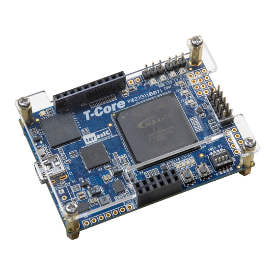
- Page 1 T-Core www.terasic.com User Manual January 14, 2020...
-
Page 2: Table Of Contents
1.5 Getting Help ............................6 Chapter 2 Using the T-Core .................... 7 2.1 Configuration of MAX 10 FPGA on T-Core ..................7 2.2 Clock Circuitry ............................. 15 2.3 Using the Push-buttons, Switches and LEDs ..................16 2.4 Using WS2812B RGB LED ......................... 18 2.5 Using 2x6 TMD GPIO Expansion Headers .................. -
Page 3: Chapter 1 Introduction
Chapter 1 Introduction The T-Core presents a robust hardware design platform built around the Intel MAX 10 FPGA. The MAX 10 FPGA is well equipped to provide cost effective, single-chip solutions in control plane or data path applications and industry-leading programmable logic for ultimate design flexibility. With MAX 10 FPGA, you can get lower power consumption / cost and higher performance. -
Page 4: T-Core System Cd
• The T-Core board • USB Mini-B Cable • Flat Ribbon Cable The T-Core System CD contains the documentation and supporting materials, including the User Manual, reference designs and device datasheets. User can download this System CD from the web (http://T-Core.terasic.com/cd). - Page 5 • 1,638 Kbits M9K Memory • 5,888 Kbits user flash memory • 144 18 × 18 Multiplier • 4 PLLs • On-Board USB Blaster II (Mini USB connector) • QSPI Flash (Support RISC-V) T-Core www.terasic.com User Manual January 14, 2020...
-
Page 6: Block Diagram Of The Board
To provide maximum flexibility for the user, all connections are made through the MAX 10 FPGA device. Thus, the user can configure the FPGA to implement any system design. Figure 1-4 Board Block Diagram T-Core www.terasic.com User Manual January 14, 2020... - Page 7 Here are the addresses where you can get help if you encounter any problem: • Terasic Inc. • 9F., No.176, Sec.2, Gongdao 5th Rd, East Dist, Hsinchu City, 30070. Taiwan • Email: support@terasic.com • Tel.: +886-3-5750-880 • Web: http://T-Core.terasic.com T-Core www.terasic.com...
-
Page 8: Using The T-Core
(CFM) which provides non-volatile storage for the bit stream. The information is retained within CFM even if the T-Core board is turned off. When the board is powered on, the configuration data in the CFM is automatically loaded into the MAX 10 FPGA. - Page 9 MAX 10 FPGA in the JTAG chain. When set to ON, the MAX10 FPGA will appear in the JTAG chain of T-Core. SW2.2 is the JTAG chain switch for RISC-V applications. If it is turned off, the application will not appear in the JTAG chain. For more information about the RISC-V application, please refer to section 3.5 for more information.
- Page 10 Click “Hardware Setup”, as circled in Figure 2-3. If it is not already turned on, turn on the USB-Blaster [USB-0] option under currently selected hardware and click “Close” to close the window. See Figure 2-4. T-Core www.terasic.com User Manual January 14, 2020...
- Page 11 Click “Auto Detect” to detect all the devices on the JTAG chain, as circled in Figure 2-5. Figure 2-5 Detect FPGA device in JTAG mode Select detected device associated with the board, as circled in Figure 2-6. T-Core www.terasic.com User Manual January 14, 2020...
- Page 12 Figure 2-6 Select 10M50DA device FPGA is detected, as shown in Figure 2-7. Figure 2-7 FPGA detected in Quartus Prime programmer T-Core www.terasic.com User Manual January 14, 2020...
- Page 13 Figure 2-8. Figure 2-8 Open the .sof file to be programmed into the FPGA device Open the “output_files” folder and select the .sof file to be programmed, as shown in Figure 2-9. T-Core www.terasic.com User Manual January 14, 2020...
- Page 14 Figure 2-9 Select the .sof file to be programmed into the FPGA device Click “Program/Configure” check box and then click “Start” button to download the .sof file into the FPGA device, as shown in Figure 2-10. Figure 2-10 Program .sof file into the FPGA device T-Core www.terasic.com User Manual January 14, 2020...
- Page 15 (CFM). Figure 2-11 High-Level Overview of Internal Configuration for MAX 10 Devices ◼ Status LED The T-Core development board includes board-specific status LEDs to indicate board status. Please refer to Table 2-2 for the description of the LED indicator.
-
Page 16: Clock Circuitry
Description I/O Standard ADC_CLK_10 PIN_N5 10 MHz clock input for ADC (Bank 3B) 3.3-V LVTTL MAX10_CLK1_50 PIN_P11 50 MHz clock input(Bank 3B) 3.3-V LVTTL MAX10_CLK2_50 PIN_N14 50 MHz clock input(Bank 3B) 3.3-V LVTTL T-Core www.terasic.com User Manual January 14, 2020... - Page 17 Every one of the switches is connected directly and individually to a pin on the MAX 10 FPGA. When the switch is in the ON position T-Core www.terasic.com User Manual...
- Page 18 LED on, and driving the pin low turns it off. Figure 2-17 is the connections between LEDs and MAX 10 FPGA. Table 2-6 list the pin assignment of user LEDs. T-Core www.terasic.com User Manual January 14, 2020...
- Page 19 Also includes a precision internal oscillator and a 12V voltage programmable constant current control part, effectively ensuring the pixel point light color height consistent. Figure 2-18 Level Shift between the REG LEDs and MAX 10 FPGA T-Core www.terasic.com User Manual January 14, 2020...
- Page 20 24bit. Pixel adopt auto reshaping transmit technology, making the pixel cascade number is not limited the signal transmission, only depends on the speed of signal transmission. T-Core www.terasic.com User Manual January 14, 2020...
- Page 21 3.3-V LVTTL ◼ Expansion Port In addition to the Built-in four RGB LEDs on the T-Core board, two 3-pin headers (JP3 and JP4) are reserved for user to expand more LED. Users can purchase the commercially RGB LED Line Pipe in series to make the application more widely available.
- Page 22 Figure 2-23 An example of a color light bar connection for an external power supply The board has one 2x6 TMD (Terasic Mini Digital) expansion header. The TMD header has 8 digital GPIO user pins connected to the MAX 10 FPGA, two 3.3V power pins and two ground pins.
- Page 23 (JP1) input. Any analog inputs signals sourced through the header JP1 are RC filtered by the Analog Front-End circuit, and the maximum allowable input voltage 2.5V per the MAX 10 FPGA ADC IP block. Figure 2-25 shows the connections between the header input and FPGA. T-Core www.terasic.com User Manual January 14, 2020...
-
Page 24: Using Qspi Flash
This device has a 4-bit data interface and uses 3.3V CMOS signaling standard. Connections between MAX 10 FPGA and Flash are shown in Figure 2-26. Table 2-11 shows the QSPI Flash pin assignments T-Core www.terasic.com User Manual January 14, 2020... - Page 25 3.3-V LVTTL QSPI_FLASH_DATA[1] PIN_P18 FLASH Data[1] 3.3-V LVTTL QSPI_FLASH_DATA[2] PIN_R18 FLASH Data[2] 3.3-V LVTTL QSPI_FLASH_DATA[3] PIN_P20 FLASH Data[3] 3.3-V LVTTL QSPI_FLASH_SCLK PIN_P19 FLASH Data Clock 3.3-V LVTTL QSPI_FLASH_CEN PIN_L22 FLASH Chip Enable 3.3-V LVTTL T-Core www.terasic.com User Manual January 14, 2020...
-
Page 26: Chapter 3 Example Designs
This chapter provides examples of advanced designs implemented by RTL or Qsys on the T-Core board. These reference designs cover the features of peripherals connected to the FPGA, such as RGB LED. All the associated files can be found in the directory \Demonstrations of T-Core System ◼ Installation of Demonstrations To install the demonstrations on your computer: Copy the folder Demonstrations to a local directory of your choice. - Page 27 RGB bit is generated according to WS2812 datasheet page 5. After all the data is transferred to WS2812 RGB LED, this module will return update_done =”1” to indicates the data transmission is completed. T-Core www.terasic.com User Manual January 14, 2020...
- Page 28 • Bitstream used: T_CORE_Default.sof, T_CORE_Default.pof ◼ Demonstration Setup and Instructions • Connect the Mini USB connector (J2) of the T-Core board to the host PC with a USB cable and install the USB-Blaster II driver if necessary. • Execute the demo batch file “test.bat” from the directory \Default\demo_batch\ •...
-
Page 29: Control Rgb Led In Nios Ii
◼ Restore Factory Configuration • Connect the mini USB connector (J2) of the T-Core board to the host PC with a USB cable and install the USB-Blaster II driver if necessary. • Execute the demo batch file “program.bat” from the directory \Default\demo_batch\ •... - Page 30 • Click “Clean” from the “Project” menu of Nios II Eclipse before compiling the reference design in the Nios II Eclipse. ◼ Demonstration Batch File • The files are located in the director: \RGBLED_NIOS\demo_batch • The folder includes the following files: T-Core www.terasic.com User Manual January 14, 2020...
- Page 31 ◼ Demonstration Setup • Quartus Prime v18.1 and Nios II v18.1 must be pre-installed on the host PC. • Connect the T-Core board to the host PC with a USB cable and install the USB-Blaster driver if necessary. • Execute the demo batch file “test.bat” from the directory \REGLED_NIOS\demo_batch •...
- Page 32 Figure 3-5 Display the progress and the result for the WS2812 test in Nios II T-Core www.terasic.com User Manual January 14, 2020...
-
Page 33: Control External Rgb Led In Nios Ii
This demonstration is very similar to the one in section 3.2. The difference is that user need to connect external RGB LEDs. Without the external power, the T-Core can control almost 10~20 external RGB LEDs, the quantities of external RGB LEDs are depending on the user’s code which is used to control the LED lightness. - Page 34 VCC, the pin marked with green box is connected to the signal, the pin marked with yellow box is connected to GND. • Connect the T-Core board to the host PC with a USB cable and install the USB-Blaster driver if necessary.
-
Page 35: Adc Measurement
Intel ADC IP to retrieve the 12-bit digitalized analog value according the channel specified by the SWITCH on the T-Core board. The input voltage can be calculated based on the 12-bit digital value. Finally, the voltage value will be displayed on the Signal Tap Logic Analyzer. - Page 36 In the demonstration, a Signal Tap is provided to display the retrieved 12-bit digitalized value and the calculated voltage for the input power to the analog input as shown in Figure 3-9. Figure 3-9 Signal Tap of ADC ◼ ◼ • Quartus Prime 18.1 Standard Edition T-Core www.terasic.com User Manual January 14, 2020...
- Page 37 Figure 3-11. In the above steps we use a self-made variable voltage output circuit. It uses the T-Core 3.3V as the power source, the output voltage is adjusted by the divider resistance and the variable resistor of the circuit, which can convert the T-Core 3.3V to a 0~2.5V analog input (to the ADC_IN0 channel).
-
Page 38: Risc-V
Any organization or individual can design their own processor based on the RISC-V architecture. Freedom E300, a RISC-V core implemented in RTL, is realized on T-Core FPGA Board. For more information about Freedom E300, user can learn more from web (https://github.com/sifive/freedom). - Page 39 PWM1 0x1003_4000 0x1003_4FFF QSPI2 0x1003_5000 0x1003_5FFF PWM2 0x2000_0000 0x3FFF_FFFF QSPI0 XIP Off-Chip 0x4000_0000 0x7FFF_FFFF Additional I/O or RAM Non-Volatile Memory 0x8000_0000 0x8001_FFFF Instruction and Data RAM On-Chip Volatile 0x8002_0000 0xFFFF_FFFF Additional RAM Memory T-Core www.terasic.com User Manual January 14, 2020...
- Page 40 The original Freedom E300 was implemented in the Scala and is not suitable for the T-Core FPGA board. We modified the Scala source code so that it can run on T-Core. Since the Verilog code generated by the Scala is hardly readable, we encapsulate it. Place the clock, reset, JTAG interface, QSPI interface, GPIO interface (including various peripherals such as UART, I2C, SPI, etc.) on the...
- Page 41 A Linux system is required to compile the RISC-V C-code project and download the binary file to the T-Core QSPI Flash. In the following demo, Ubuntu 16.04 is used and recommended. Quartus Prime (or Quartus Programmer), USB Blaster II Driver, RISC-V BSP should be installed on the host PC before running the demo.
- Page 42 Figure 3-14 Download Quartus Prime 18.1 Standard Edition ◆ USB-Blaster II Driver The Intel Quartus Prime software accesses USB-Blaster II through USB file system. After installing the Quartus Prime software, user need to change the port permissions. T-Core www.terasic.com User Manual January 14, 2020...
- Page 43 ATTRS{idProduct}=="6810", MODE="0666" ◆ T-Core RISC-V BSP After Quartus Prime and USB-Blaster II driver are installed, please download the T-Core RISC-V BSP (TCORE-RISCV-FreedomE300.tar.gz) from the web (http://T-Core.terasic.com/cd). Then, decompress the file using command: tar -zxvf TCORE-RISCV-FreedomE300.tar.gz. So far, you can see TCORE-RISCV-FreedomE300 file. For more information about T-Core RISC-V BSP, please refer following table.
- Page 44 Figure 3-15 SW2 Setting Make sure Quartus Prime 18.1 Standard Edition is installed to the host PC. Connect the T-Core board (J2) to the host PC via the USB cable. Go to TCORE-RISCV-FreedomE300/Quartus_Project/TCORE_FreedomE300/demo_batch directory using command: cd TCORE-RISCV-FreedomE300/Quartus_Project/TCORE_FreedomE300/demo_batch. Execute command: sh programming_pof.sh to configure the FPGA.
- Page 45 Figure 3-17 Compile and download process T-Core www.terasic.com User Manual January 14, 2020...
- Page 46 Figure 3-19, to solve Figure 3-18 The error encountered when programming QSPI Flash Figure 3-19 Fix the error encountered when programming QSPI Flash T-Core www.terasic.com User Manual January 14, 2020...
- Page 47 QSPI Flash. After the reset operation, the RISC-V core will execute the demo program. You can program new software into board with the SDK, but the FPGA image will not be modified. T-Core www.terasic.com User Manual January 14, 2020...
-
Page 48: Programming The Configuration Flash Memory
The following sections provide a quick overview of the design flow. Please note that if you are using the dual image boot function on the T-Core board, you will need to solder the JP2 2-pin header (pitch 0.100" (2.54 mm)) by yourself. -
Page 49: Internal Configuration
1, are stored in the CFM. The MAX 10 device loads either one of the application configuration image from the CFM. If an error occurs, the device will automatically load the other application configuration image. Remote System Upgrade Flow for MAX 10 Devices is shown in Figure 4-3. T-Core www.terasic.com User Manual January 14, 2020... - Page 50 5. Reconfiguration is triggered by the following actions: • Driving the nSTATUS low externally • Asserting internal or external nCONFIG low • Asserting RU_nCONFIG low (Avalon-MM interface signal) T-Core www.terasic.com User Manual January 14, 2020...
-
Page 51: Using Dual Compressed Images
Figure 4-4 Select Qsys menu and click 2. Please choose Library > Basic Function> Configuration and Programming > Dual Configuration Intel FPGA IP to open wizard of adding dual boot IP. See Figure 4-5 Figure 4-6. T-Core www.terasic.com User Manual January 14, 2020... - Page 52 Figure 4-5 Select Dual Configuration Intel FPGA IP and click. Figure 4-6 Open wizard and click Finish. T-Core www.terasic.com User Manual January 14, 2020...
- Page 53 4. Click “Generate HDL..” button and click Generate button when popping a window as shown Figure 4-8. Click Save it as dual_boot.qsys and the generation start. If there is no error in the generation, the window will show successful as shown in Figure 4-9. T-Core www.terasic.com User Manual January 14, 2020...
- Page 54 5. Click Close and Finish to return to the Quartus window and add the dual_boot qsys into the top file as shown in Figure 4-10, and add the dual_boot.qip file to the project and save. T-Core www.terasic.com User Manual January 14, 2020...
- Page 55 2. Click Device and Pin Opinions to open the Device and Pin Opinions windows, and in the Configuration tab, Set the Configuration Scheme to Internal Configuration and the Configuration Mode to Dual Compressed Images. Check the Option of Generate compressed bitstreams. shown in Figure 4-12. T-Core www.terasic.com User Manual January 14, 2020...
- Page 56 .pof into configuration flash memory (CFM) through the JTAG interface. Convert .SOF File to .POF File 1. Choose Convert Programming Files from the File menu of Quartus Prime to open new window, as shown in Figure 4-13. T-Core www.terasic.com User Manual January 14, 2020...
- Page 57 4. Browse to the target directory from the File name field and specify the name of output file. 5. Click on the SOF data in the section of Input files to convert, as shown in Figure 4-14. T-Core www.terasic.com User Manual January 14, 2020...
- Page 58 7. Click Add Sof Page to add Page_1 and click Add File, Select the LED1_blink.sof to be the .sof data of Page_1 as shown in Figure 4-15. 8. Click Generate. These project files can be found in the CD directory: \Demonstrations\Dual_boot\ T-Core www.terasic.com User Manual January 14, 2020...
- Page 59 Now, you can set the BOOT_SEL by JP2, you will find if you open JP2 (BOOT_SEL = 0), the LED0 Blink function would show. Power off the board, insert the jumper to JP2 (BOOT_SEL = 1), then power on, you would find the LED1 Blink function show. T-Core www.terasic.com User Manual...
- Page 60 Figure 4-16 Hardware setup window Figure 4-17 Programmer window with dual_boot.pof file T-Core www.terasic.com User Manual January 14, 2020...
-
Page 61: Usb Blaster Ii Cable Feature
Chapter 5 USB Blaster II Cable Feature The additional feature of T-Core is that it can be used as a USB blaster II to allow users to program other Intel FPGA boards from the host PC. As shown in Figure 5-1, users can connect to the external JTAG header (J1) of the T-Core using a flat ribbon cable. - Page 62 The following example demonstrates that use the T-Core to connect the JTAG interface of the Terasic's DE10-Pro Stratix 10 development board and program .sof file into the FPGA via JTAG interface. 1. Connect the flat ribbon cable to the J1 of the T-Core board, as shown in Figure 5-4. The red line represents the connection line of pin 1, which needs to be connected to the pin of J1.
- Page 63 5-5. Figure 5-5 The flat ribbon cable connected to the T-Core board 3. Using mini USB cable to connected J2 of the T-Core board and the host PC. 4. Power the DE10-Pro board. 5. Open the Quartus programmer on the host PC, press "Hardware Setup" and select T-Core [USB-*].
- Page 64 Figure 5-6 Using T-Core board to program the DE10-Pro 6. Select a .sof of the DE10-Pro project and download it. shows the success of the T-Core program Stratix 10 FPGA, as shown in Figure 5-7. T-Core www.terasic.com User Manual January 14, 2020...
- Page 65 Figure 5-7 Using T-Core board to program the DE10-Pro T-Core www.terasic.com User Manual January 14, 2020...
- Page 66 Change Log 2019.07 V1.0 Initial Version (Preliminary) ⚫ Modify the SW2 setting description for Figure 3-16. 2020.01 V1.1 ⚫ Change blaster name from DE-Core to T-Core Copyright © 2020 Terasic Inc. All rights reserved. T-Core www.terasic.com User Manual January 14, 2020...
Need help?
Do you have a question about the T-Core and is the answer not in the manual?
Questions and answers