Table of Contents
Advertisement
Quick Links
Advertisement
Table of Contents

Related Manuals for Terasic TR10a-LPQ


Summary of Contents for Terasic TR10a-LPQ
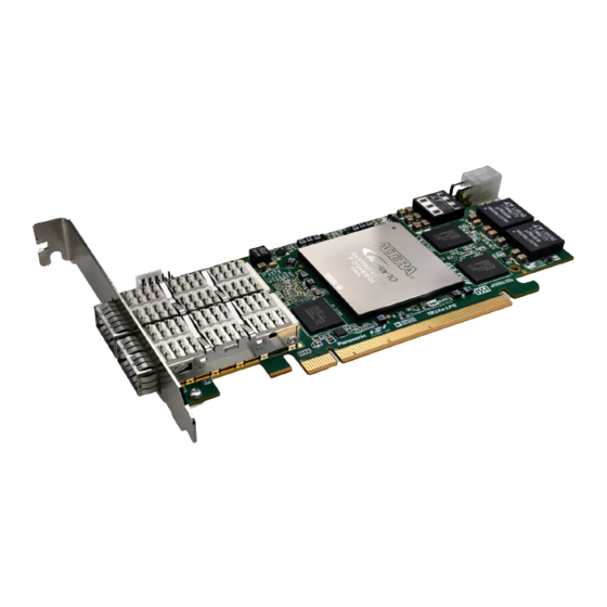
- Page 1 TR10a-LPQ User Manual www.terasic.com December 2018...
-
Page 2: Table Of Contents
6.6 PCIe Design: PCIe_Fundamental_x2 ..........97 Chapter 7 Transceiver Verification ............105 7.1 Function of the Transceiver Test Code ..........105 7.2 Loopback Fixture ................105 7.3 Testing ....................107 Chapter 8 TR10a-LPQ Dashboard ............109 TR10a-LPQ User Manual www.terasic.com December 2018... - Page 3 8.1 Dashboard Connected via USB Blaster II ........... 110 8.2 Dashboard Connected via UART ............116 Additional Information ................128 Getting Help .................... 128 TR10a-LPQ User Manual www.terasic.com December 2018...
-
Page 4: Chapter 1 Overview
The Arria® 10 GX FPGA features integrated transceivers that transfer at a maximum of 12.5 Gbps, allowing the TR10a-LPQ to be fully compliant with version 3.0 of the PCI Express standard, as well as allowing an ultra low-latency, straight connections to two external 40G QSFP+ modules. -
Page 5: Key Features
1.2 Key Features The following hardware is implemented on the TR10a-LPQ board: ◼ FPGA ⚫ Altera Arria® 10 GX FPGA (10AX115N2F45E1SG) ◼ FPGA Configuration ⚫ On-Board USB Blaster II for FPGA programming ⚫ Fast passive parallel (FPPx16) configuration via MAX II CPLD and flash memory ◼... -
Page 6: Block Diagram
1.3 Block Diagram Figure 1-1 shows the block diagram of the TR10a-LPQ board. To provide maximum flexibility for the users, all key components are connected to the Arria 10 GX FPGA device. Thus, users can configure the FPGA to implement any system design. - Page 7 ◼ Four QSFP+ ports ⚫ Two QSFP+ connector (40 Gbps+) ◼ Dual PCI Express x8 edge connector ⚫ Support for Dual PCIe x8 Gen1/2/3 ⚫ Edge connector for PC motherboard with x16 PCI Express slot TR10a-LPQ User Manual www.terasic.com December 2018...
- Page 8 ◼ System Monitor and Control Temperature sensor ⚫ ⚫ Fan control ⚫ Power monitor ⚫ UART to USB for board management ◼ Power Source ⚫ PCI Express 4-pin DC 12V power ⚫ PCI Express edge connector power TR10a-LPQ User Manual www.terasic.com December 2018...
-
Page 9: Chapter 2 Board Components
Chapter 2 Board Components his chapter introduces all the important components on the TR10a-LPQ. 2.1 Board Overview Figure 2-1 Figure 2-2 are the top and bottom view of the TR10a-LPQ development board. It depicts the layout of the board and indicates the location of the connectors and key components. -
Page 10: Configuration, Status And Setup
Launch Quartus Prime programmer and make sure the USB-Blaster II is detected. ⚫ In Quartus Prime Programmer, add the configuration bit stream file (.sof), check the associated “Program/Configure” item, and click “Start” to start FPGA programming. TR10a-LPQ User Manual www.terasic.com December 2018... - Page 11 The FPGA Board development board includes board-specific status LEDs to indicate board status as shown in Figure 2-3. Please refer to Table 2-1 for the description of the LED indicator. Figure 2-3 Status LED on the TR10a-LPQ Table 2-1 Status LED Board LED Name Description Reference 12-V Power Illuminates when 12-V power is active.
- Page 12 The PCI Express Control DIP switch (S1) is provided to enable or disable different configurations of the PCIe Connector. Table 2-2 lists the switch controls and description. Figure 2-4 Setup PCI Express Control DIP switch TR10a-LPQ User Manual www.terasic.com December 2018...
- Page 13 FPGA. Setting Position 4 of S1 to “1” (down position) specifies the default factory image to be loaded, as shown in Figure 2-6. Setting Position 4 of S1 to “0” (up position) specifies the TR10a-LPQ to load a user-defined image, as shown in Figure 2-7. TR10a-LPQ User Manual www.terasic.com...
-
Page 14: General User Input/Output
Arria 10 GX device. Each push-button provides a high logic level or a low logic level when it is not pressed or pressed, respectively. Table 2-3 lists the board references, signal names and their corresponding Arria 10 GX device pin numbers. TR10a-LPQ User Manual www.terasic.com December 2018... - Page 15 When a dip switch is in the DOWN position or the UPPER position, it provides a high logic level or a low logic level to the Arria 10 GX FPGA, respectively, as shown in Figure 2-9. TR10a-LPQ User Manual www.terasic.com December 2018...
- Page 16 Figure 2-10. A list of the pin names on the FPGA that are connected to the LEDs is given in Table 2-5. TR10a-LPQ User Manual www.terasic.com December 2018...
-
Page 17: Temperature Sensor And Fan Control
LED3 1.8-V PIN_V10 2.4 Temperature Sensor and Fan Control The TR10a-LPQ has an automatic management system for the temperature of the FPGA, the fan speed, and the power supply of the FPGA. As shown in Figure 2-11. The MAX10 FPGA is the main control device on the board. -
Page 18: Power Monitor
FPGA to avoid damage caused by excessive FPGA temperature. Figure 2-11 The Temperature, Fan Speed and FPGA power control system 2.5 Power Monitor The TR10a-LPQ has implemented a power monitor chip to monitor the board input power voltage and current. Figure 2-12 shows the connection between the power monitor chip and the Arria 10 GX FPGA. -
Page 19: Clock Circuit
2.6 Clock Circuit The development board includes four 50 MHz oscillators and two programmable clock generators. Figure 2-13 shows the default frequencies of on-board all external clocks going to the Arria 10 GX FPGA. TR10a-LPQ User Manual www.terasic.com December 2018... - Page 20 PIN_AP34 User Application CLK_50_B2I 1.8V PIN_C30 User Application CLK_50_B2J 50.0 MHz 1.8V PIN_W36 User Application CLK_50_B3C 1.8V PIN_AK12 User Application CLK_50_B3D 1.8V PIN_AJ11 User Application CLK_100_B2J 100.0MHz 1.8V PIN_AC32 User Application OSC_100_CLKUSR 100.0MHz 1.8V PIN_AV26 User-supplied TR10a-LPQ User Manual www.terasic.com December 2018...
- Page 21 Pin Number Si5340A_I2C_SCL 1.8-V PIN_F24 I2C bus, connected with Si5340A Si5340A_I2C_SDA 1.8-V PIN_G24 Si5340A reset Si5340A_RST 1.8-V PIN_C27 signal Si5340A Si5340A interrupt (U2) Si5340A_INTR 1.8-V PIN_C28 signal Si5340A output Si5340A_OE_n 1.8-V PIN_AP39 enable signal TR10a-LPQ User Manual www.terasic.com December 2018...
-
Page 22: Flash Memory
Address bus 1.8-V PIN_AE14 FLASH_A2 Address bus 1.8-V PIN_AT7 FLASH_A3 Address bus 1.8-V PIN_AC11 FLASH_A4 Address bus 1.8-V PIN_AC13 FLASH_A5 Address bus 1.8-V PIN_AC12 FLASH_A6 Address bus 1.8-V PIN_AF14 FLASH_A7 Address bus 1.8-V PIN_AD13 TR10a-LPQ User Manual www.terasic.com December 2018... - Page 23 Data bus 1.8-V PIN_AN10 FLASH_D9 Data bus 1.8-V PIN_AR12 FLASH_D10 Data bus 1.8-V PIN_AP10 FLASH_D11 Data bus 1.8-V PIN_AP11 FLASH_D12 Data bus 1.8-V PIN_AT10 FLASH_D13 Data bus 1.8-V PIN_AP9 FLASH_D14 Data bus 1.8-V PIN_AU7 TR10a-LPQ User Manual www.terasic.com December 2018...
-
Page 24: Qdrii+ Sram
1.8-V HSTL Class I PIN_P11 QDRIIA_A5 Address bus[5] 1.8-V HSTL Class I PIN_N11 QDRIIA_A6 Address bus[6] 1.8-V HSTL Class I PIN_M9 QDRIIA_A7 Address bus[7] 1.8-V HSTL Class I PIN_M8 QDRIIA_A8 Address bus[8] 1.8-V HSTL Class I PIN_N7 TR10a-LPQ User Manual www.terasic.com December 2018... - Page 25 Read Data bus[0] 1.8-V HSTL Class I PIN_H12 QDRIIA_Q1 Read Data bus[1] 1.8-V HSTL Class I PIN_K12 QDRIIA_Q2 Read Data bus[2] 1.8-V HSTL Class I PIN_J14 QDRIIA_Q3 Read Data bus[3] 1.8-V HSTL Class I PIN_H11 TR10a-LPQ User Manual www.terasic.com December 2018...
- Page 26 Table 2-11 QDRII+ SRAM B Pin Assignments, Schematic Signal Names, and Functions Schematic Arria 10 GX Pin Description I/O Standard Signal Name Number QDRIIB_A0 Address bus[0] 1.8-V HSTL Class I PIN_L16 QDRIIB_A1 Address bus[1] 1.8-V HSTL Class I PIN_L15 TR10a-LPQ User Manual www.terasic.com December 2018...
- Page 27 Write data bus[11] 1.8-V HSTL Class I PIN_L21 QDRIIB_D12 Write data bus[12] 1.8-V HSTL Class I PIN_L20 QDRIIB_D13 Write data bus[13] 1.8-V HSTL Class I PIN_F20 QDRIIB_D14 Write data bus[14] 1.8-V HSTL Class I PIN_F19 TR10a-LPQ User Manual www.terasic.com December 2018...
- Page 28 Write Port Select 1.8-V HSTL Class I PIN_K16 QDRIIB_DOFF_n PLL Turn Off 1.8-V HSTL Class I PIN_H16 On-Die Termination QDRIIB_ODT 1.8-V HSTL Class I PIN_M17 Input QDRIIB_QVLD Valid Output 1.8-V HSTL Class I PIN_K23 TR10a-LPQ User Manual www.terasic.com December 2018...
- Page 29 Write data bus[3] 1.8-V HSTL Class I PIN_D35 QDRIIC_D4 Write data bus[4] 1.8-V HSTL Class I PIN_E37 QDRIIC_D5 Write data bus[5] 1.8-V HSTL Class I PIN_F39 QDRIIC_D6 Write data bus[6] 1.8-V HSTL Class I PIN_F37 TR10a-LPQ User Manual www.terasic.com December 2018...
- Page 30 1.8-V HSTL Class I PIN_F34 Byte Write select[0] QDRIIC_BWS_n1 1.8-V HSTL Class I PIN_C37 Byte Write select[1] Differential 1.8-V PIN_F32 QDRIIC_K_p HSTL Class I Clock P Differential 1.8-V PIN_E32 QDRIIC_K_n HSTL Class I Clock N TR10a-LPQ User Manual www.terasic.com December 2018...
- Page 31 1.8-V HSTL Class I PIN_BC18 QDRIID_A18 Address bus[18] 1.8-V HSTL Class I PIN_BD18 QDRIID_A19 Address bus[19] 1.8-V HSTL Class I PIN_BD15 QDRIID_A20 Address bus[20] 1.8-V HSTL Class I PIN_BD16 QDRIID_A21 Address bus[21] 1.8-V HSTL Class I PIN_BC16 TR10a-LPQ User Manual www.terasic.com December 2018...
- Page 32 Read Data bus[13] 1.8-V HSTL Class I PIN_BB14 QDRIID_Q14 Read Data bus[14] 1.8-V HSTL Class I PIN_AY14 QDRIID_Q15 Read Data bus[15] 1.8-V HSTL Class I PIN_AU13 QDRIID_Q16 Read Data bus[16] 1.8-V HSTL Class I PIN_AW13 TR10a-LPQ User Manual www.terasic.com December 2018...
- Page 33 1.8-V HSTL Class I PIN_BA32 QDRIIE_A11 Address bus[11] 1.8-V HSTL Class I PIN_BB32 QDRIIE_A12 Address bus[12] 1.8-V HSTL Class I PIN_AY31 QDRIIE_A13 Address bus[13] 1.8-V HSTL Class I PIN_BA31 QDRIIE_A14 Address bus[14] 1.8-V HSTL Class I PIN_AV28 TR10a-LPQ User Manual www.terasic.com December 2018...
- Page 34 Read Data bus[6] 1.8-V HSTL Class I PIN_BC33 QDRIIE_Q7 Read Data bus[7] 1.8-V HSTL Class I PIN_AY33 QDRIIE_Q8 Read Data bus[8] 1.8-V HSTL Class I PIN_AY32 QDRIIE_Q9 Read Data bus[9] 1.8-V HSTL Class I PIN_AV31 TR10a-LPQ User Manual www.terasic.com December 2018...
-
Page 35: Qspf+ Ports
Arria 10 GX FPGA device and transform them to optical signals. The board includes cage assemblies for the QSFP+ connectors. Figure 2-15 shows the connections between the QSFP+ and Arria 10 GX FPGA. TR10a-LPQ User Manual www.terasic.com December 2018... - Page 36 Module Present 1.8V PIN_AT37 Table 2-16 QSFP+ B Pin Assignments, Schematic Signal Names, and Functions Schematic Arria 10 GX Description I/O Standard Signal Name Pin Number QSFPB_TX_P0 Transmitter data of channel 0 1.4-V PCML PIN_AP1 TR10a-LPQ User Manual www.terasic.com December 2018...
-
Page 37: Pci Express
The PCIE_REFCLK_p signal is a differential input that is driven from the PC motherboard on this board through the PCIe edge connector. A DIP switch (S1) is connected to the PCI Express to allow different configurations to enable a x1, x4, or x8 TR10a-LPQ User Manual www.terasic.com December... - Page 38 1.4-V PCML PIN_AR42 PCIE_RX_p2 Add-in card receive bus 1.4-V PCML PIN_AN42 PCIE_RX_p3 Add-in card receive bus 1.4-V PCML PIN_AL42 PCIE_RX_p4 Add-in card receive bus 1.4-V PCML PIN_AJ42 PCIE_RX_p5 Add-in card receive bus 1.4-V PCML PIN_AG42 TR10a-LPQ User Manual www.terasic.com December 2018...
- Page 39 PCIE2_RX_p5 Add-in card receive bus 1.4-V PCML PIN_D40 PCIE2_RX_p6 Add-in card receive bus 1.4-V PCML PIN_C42 PCIE2_RX_p7 Add-in card receive bus 1.4-V PCML PIN_B40 PCIE2_REFCLK_p Motherboard reference clock HCSL PIN_Y40 PCIE2_PERST_n Reset 1.8-V PIN_AR24 TR10a-LPQ User Manual www.terasic.com December 2018...
-
Page 40: 2X5 Timing Header
GPIO_CLK0 and GPIO_CLK1 are connected to FPGA dedicated clock input and can be configured as two single-ended clock signals or one differential clock signal. Users can use Terasic defined RS422-RJ45 board and TUB (Timing and UART Board) for RS422 and external clock inputs/UART applications. -
Page 41: Chapter 3 Flash Programming
Power on the FPGA board or press the MAX_RST button if board is already powered on, When the configuration is completed, the green Configure Done LED will light. If there is an error, the red Configure Error LED will light. TR10a-LPQ User Manual www.terasic.com December 2018... -
Page 42: Cfi Flash Memory Map
Figure 3-2 Configuration Image Selection CFI Flash Memory Map The TR10a-LPQ has one 1-Gbit, 16-bit data width, CFI compatible synchronous flash device for non-volatile storage of the FPGA configuration data, user Nios II code, and user data. Both MAX V CPLD and Stratix 10 GX FPGA can access this Flash device. -
Page 43: Flash Example Designs
Demonstration folder under the System CD as shown in Table 3-2. Table 3-2 Flash Example Design Example Folder Description Flash_Programming This is the flash programming design. It is used to write data into FLASH by a Quartus Programmer. TR10a-LPQ User Manual www.terasic.com December 2018... -
Page 44: Flash_Programming Example
“CFI Parallel Flash” is selected. Figure 3-5 shows the Flash Interface Setting. “CFI 1 Gbit” is selected. The Flash_Programming.sof generated by this program is used in the flash programming batch files located in the Flash_Restore folder. TR10a-LPQ User Manual www.terasic.com December 2018... -
Page 45: Flash_Factory Example
Figure 3-7. Finally, developers need to uncheck the allow_code_at_reset and enable_alt_load options in the BSP editor under of Nios II IDE tool (Nios II Software Builder Tools for Eclipse) as shown in Figure 3-8. TR10a-LPQ User Manual www.terasic.com December 2018... - Page 46 Figure 3-6 Flash Controller Settings in Platform Designer (formerly Qsys) Figure 3-7 Factory Software Reset Vector Settings for NIOS II Processor TR10a-LPQ User Manual www.terasic.com December 2018...
-
Page 47: Flash_User Example
Nios II processor component and the LED control code in Nios II program. The User Software Location 0x05E40000 is used as Reset Vector as shown in Figure 3-9. Figure 3-9 User Software Reset Vector Settings for NIOS II Processor TR10a-LPQ User Manual www.terasic.com December 2018... -
Page 48: Flash_Tool Example
The factory subfolder includes the .sof & .elf files generated by the Flash_Factory project. The user subfolder includes the .sof & .elf files generated by the Flash_User project. Flash_Programming.sof is generated by the Flash_Programming project. TR10a-LPQ User Manual www.terasic.com December... -
Page 49: Restore Factory Settings
Make sure the Nios II EDS and USB-Blaster II driver are installed. Make sure the FPGA board and PC are connected with an USB Cable. Power on the FPGA board. Copy the “Demonstrations/Flash_Restore” folder under the CD to your PC’s TR10a-LPQ User Manual www.terasic.com December 2018... - Page 50 The factory subfolder includes Flash_Programming.sof and NIOS_APP.elf files generated Flash_Factory project, user subfolder includes Flash_Programming.sof and NIOS_APP.elf files generated by Flash_User project. The Flash_Programming.sof under the Flash_Restore folder is used to program flash by Quartus Programmer. TR10a-LPQ User Manual www.terasic.com December 2018...
-
Page 51: Peripheral Reference Design
The source codes and tool of these examples are all available on the System 4.1 Configure Si5340A in RTL There is a Silicon Labs Si5340A clock generators on TR10a-LPQ FPGA board can provide adjustable frequency reference clock (See Figure 4-1) for QSFP+ connectors and memory modules (QDR-II+). - Page 52 Si5340A Controller IP. Table 4-1 Si5340A Controller Instruction Ports Port Direction Description iCLK input System Clock (50Mhz) Synchronous Reset iRST_n input (0: Module Reset, 1: Normal) iStart input Start to Configure(positive edge TR10a-LPQ User Manual www.terasic.com December 2018...
- Page 53 Si5340A Channel Clock Frequency (MHz) Input Setting 4'h0 644.53125 4'h1 322.265625 4'h2 4'h3 4'h4 Table 4-3 Si5340A Controller Reference Clock Frequency Setting for Memory iMEM_REFCLK Si5340A Channel Clock Frequency (MHz) Input Setting TR10a-LPQ User Manual www.terasic.com December 2018...
- Page 54 Silicon Labs. This tool can help users to set the Si5340A’s output frequency of each channel through the GUI interface, and it will automatically calculate the Register parameters required for each frequency. The tool download link: http://www.silabs.com/products/clocksoscillators/pages/timing-software- development-tools.aspx TR10a-LPQ User Manual www.terasic.com December 2018...
- Page 55 Figure 4-3 ClockBuilder Pro Wizard After the installation, select Si5340, and configure the input frequency and output frequency as shown in Figure 4-4. Figure 4-4 Define Output Clock Frequencies on ClockBuilder Pro Wizard TR10a-LPQ User Manual www.terasic.com December 2018...
- Page 56 Figure 4-5 Open Design Report on ClockBuilder Pro Wizard Open Si5340A control IP sub-module “si5340a_i2c_reg_controller.v “ as shown Figure 4-6, refer Design Report parameter to modify sub-module corresponding register value (See Figure 4-7). Figure 4-6 Sub-Module file "si5340a_i2c_reg_controller.v" TR10a-LPQ User Manual www.terasic.com December 2018...
-
Page 57: Nios Ii Control For Si5340
PIO controller, and programmed through I2C protocol which is implemented in the C code. The I2C pins from chip are connected to Qsys System Interconnect Fabric through PIO controllers. The Nios II program toggles the PIO controller to implement TR10a-LPQ User Manual www.terasic.com December... - Page 58 In the external PLL(Si5340A) programming test, the program will program the PLL first, and subsequently will use TERASIC QSYS custom CLOCK_COUNTER IP to count the clock count in a specified period to check whether the output frequency is changed as configured.
- Page 59 Make sure Quartus Prime 18.0 and Nios II EDS are installed on your PC. ⚫ ⚫ Power on the TR10a-LPQ board. ⚫ Use the USB Cable to connect your PC and the FPGA board and install USB Blaster II driver if necessary.
-
Page 60: Memory Reference Design
The five QDRII+ SRAM controllers are configured as a 72Mb controller. The QDRII+ SRAM IP generates a 550MHz clock as memory clock and a half-rate system clock, 275MHz, for the TR10a-LPQ User Manual www.terasic.com December 2018... - Page 61 The Avalon bus read/write test (RW_test) modules read and write the entire memory space of each QDRII+ SRAM through the Avalon interface of each controller. In this project, the RW_test module will first write the entire memory and then compare the TR10a-LPQ User Manual www.terasic.com December...
- Page 62 CPU_RESET_n is held down, all the LEDs will be turned off. All LEDs should turn back on to indicate test passes upon the release of CPU_RESET_n. ⚫ If any LED is not lit up after releasing CPU_RESET_n, it indicates the TR10a-LPQ User Manual www.terasic.com December 2018...
-
Page 63: Qdrii+ Sram Test By Nios Ii
Each QDRII+ controller is configured as a 8 MB QDRII+ controller. Nios II processor is used to perform memory test. The Nios II program is running in the On-Chip Memory. A PIO Controller is used to monitor buttons status which is used to trigger starting memory testing. TR10a-LPQ User Manual www.terasic.com December 2018... - Page 64 ◼ Nios II Project Compilation Before you attempt to compile the reference design under Nios II Eclipse, make sure the project is cleaned first by clicking ‘Clean’ from the ‘Project’ menu of Nios II Eclipse. TR10a-LPQ User Manual www.terasic.com December...
- Page 65 ⚫ Press Button1~Button0 of the FPGA board to start SRAM verify process. Press Button0 for continued test. ⚫ The program will display progressing and result information, as shown in Figure 5-3. TR10a-LPQ User Manual www.terasic.com December 2018...
- Page 66 Figure 5-3 Progress and Result Information for the QDRII+ Demonstration TR10a-LPQ User Manual www.terasic.com December 2018...
-
Page 67: Pci Express Reference Design
It consists of two primary components: FPGA System and PC System. The FPGA System is developed based on Arria 10 Hard IP for PCI Express with Avalon-MM DMA. The application software on the PC side is developed by Terasic based on Altera’s PCIe kernel mode driver. -
Page 68: Pc Pci Express Software Sdk
PCIe vender ID (VID) and device ID (DID) in the driver INF file accordingly. Express Library implemented single named "TERASIC_PCIE_AVMM.DLL". This file is a 64-bit DLL. With the DLL is exported to the software API, users can easily TR10a-LPQ User Manual www.terasic.com December 2018... -
Page 69: Pci Express Software Stack
Windows. The PCI Express driver incorporated in the DLL library is called "TERASIC_PCIE_AVMM.dll". Users can develop their applications based on this DLL. The "altera_pcie_win_driver.sys" kernel driver is provided by Altera. Figure 6-2 PCI Express Software Stack TR10a-LPQ User Manual www.terasic.com December 2018... - Page 70 WdfCoinstaller01011.dll To install the PCI Express driver, please execute the steps below: 1. Install the TR10a-LPQ on the PCIe slot of the host PC 2. Make sure Altera Programmer and USB-Blaster II driver are installed 3. Execute test.bat in "CDROM\Demonstrations\PCIe_Fundamental\demo_batch"...
- Page 71 Figure 6-4. Figure 6-4 Dialog of Browse my computer for driver software 7. In the Browse for driver software on your computer dialog, click the Browse TR10a-LPQ User Manual www.terasic.com December 2018...
- Page 72 Figure 6-5 Browse for driver software on your computer 8. When the Windows Security dialog appears, as shown Figure 6-6, click the Install button. Figure 6-6 Click Install in the dialog of Windows Security TR10a-LPQ User Manual www.terasic.com December 2018...
- Page 73 9. When the driver is installed successfully, the successfully dialog will appears, as shown in Figure 6-7. Click the Close button. Figure 6-7 Click Close when the installation of Altera PCI API Driver is complete TR10a-LPQ User Manual www.terasic.com December 2018...
- Page 74 DLL, please refer to the PCIe fundamental example below. Call the SDK API to implement the desired application. Users can easily communicate with the FPGA through the PCIe bus through the "TERASIC_PCIE_AVMM.DLL" API. The details of API are described below: TR10a-LPQ User Manual www.terasic.com December 2018...
- Page 75 Users need to call PCIE_Close to release handle once the handle is no more used. ◼ PCIE_Close Function: Close a handle associated to the PCIe card. Prototype: void PCIE_Close( PCIE_HANDLE hPCIE); Parameters: hPCIE: A PCIe handle return by PCIE_Open function. Return Value: None. ◼ PCIE_Read32 Function: TR10a-LPQ User Manual www.terasic.com December 2018...
- Page 76 Return TRUE if read data is successful; otherwise FALSE is returned. ◼ PCIE_Write32 Function: Write a 32-bit data to the FPGA Board. Maximal write size is (4GB-1) bytes. Prototype: bool PCIE_Write32( PCIE_HANDLE hPCIE, PCIE_BAR PcieBar, PCIE_ADDRESS PcieAddress, DWORD dwData); TR10a-LPQ User Manual www.terasic.com December 2018...
- Page 77 A pointer to a memory buffer to retrieved the data from FPGA. The size of buffer should be equal or larger the dwBufSize. dwBufSize: Specify the byte number of data retrieved from FPGA. Return Value: Return TRUE if read data is successful; otherwise FALSE is returned. ◼ PCIE_DmaWrite TR10a-LPQ User Manual www.terasic.com December 2018...
- Page 78 PCIE_HANDLE hPCIE, DWORD Offset, DWORD *pdwData Parameters: hPCIE: A PCIe handle return by PCIE_Open function. Offset: Specify the target byte of offset in PCIe configuration table. pdwData: A 4-bytes buffer to retrieve the 32-bit data. TR10a-LPQ User Manual www.terasic.com December 2018...
-
Page 79: Pcie Design - Fundamental
1. Install the FPGA board on your PC as shown in Figure 6-9. Figure 6-9 FPGA board installation on PC 2. Configure FPGA with PCIe_Fundamental.sof by executing the test.bat. 3. Install PCIe driver if necessary. The driver is located in the folder: TR10a-LPQ User Manual www.terasic.com December 2018... - Page 80 5. Make sure the Windows has detected the FPGA Board by checking the Windows Control panel as shown in Figure 6-10. Figure 6-10 Screenshot for PCIe Driver 6. Goto windows_app folder, execute PCIE_FUNDMENTAL.exe. A menu will appear as shown in Figure 6-11. TR10a-LPQ User Manual www.terasic.com December 2018...
- Page 81 7. Type 0 followed by a ENTERY key to select Led Control item, then input 15 (hex 0x0f) will make all led on as shown in Figure 6-12. If input 0(hex 0x00), all led will be turn off. TR10a-LPQ User Manual www.terasic.com December 2018...
- Page 82 Figure 6-13. Figure 6-13 Screenshot of Button Status Report 9. Type 2 followed by an ENTERY key to select DMA Testing item. The DMA test result will be report as shown in Figure 6-14. TR10a-LPQ User Manual www.terasic.com December 2018...
- Page 83 PIO controller is used to control the LED and monitor the Button Status, and the On- Chip memory is used for performing DMA testing. The PIO controllers and the On-Chip memory are connected to the PCI Express Hard IP controller through the Memory- Mapped Interface. TR10a-LPQ User Manual www.terasic.com December 2018...
- Page 84 Implement dynamically load for TERAISC_PCIE_AVMM.DLL PCIE.h TERASIC_PCIE_AVMM.h SDK library file, defines constant and data structure The main program PCIE_FUNDAMENTAL.cpp includes the header file "PCIE.h" and defines the controller address according to the FPGA design. TR10a-LPQ User Manual www.terasic.com December 2018...
- Page 85 The LED control is implemented by calling PCIE_Write32 API, as shown below: The button status query is implemented by calling the PCIE_Read32 API, as shown below: The memory-mapped memory read and write test is implemented by PCIE_DmaWrite and PCIE_DmaRead API, as shown below: TR10a-LPQ User Manual www.terasic.com December 2018...
-
Page 86: Pcie Design - Qdrii
3. Install PCIe driver if necessary. 4. Restart Windows 5. Make sure the Windows has detected the FPGA Board by checking the Windows Control panel. 6. Goto windows_app folder, execute PCIE_QDR.exe. A menu will appear as shown Figure 6-16. TR10a-LPQ User Manual www.terasic.com December 2018... - Page 87 7. Type 2 followed by a ENTERY key to select Link Info item. The PICe link information will be shown as in Figure 6-17. Gen3 link speed and x8 link width are expected. Figure 6-17 Screenshot of Link Info TR10a-LPQ User Manual www.terasic.com December 2018...
- Page 88 Figure 6-18 Screenshot of On-Chip Memory DMA Test Result 9. Type 4 followed by an ENTERY key to select DMA QDRII-A Memory Test item. The DMA write and read test result will be report as shown in Figure 6-19. TR10a-LPQ User Manual www.terasic.com December 2018...
- Page 89 Figure 6-19 Screenshot of QDRII-A Memory DAM Test Result 10. Type 5 followed by an ENTERY key to select DMA QDRII-B Memory Test item. The DMA write and read test result will be report as shown in Figure 6-20. TR10a-LPQ User Manual www.terasic.com December 2018...
- Page 90 Figure 6-20 Screenshot of QDRII-B Memory DAM Test Result 11. Type 6 followed by an ENTERY key to select DMA QDRII-C Memory Test item. The DMA write and read test result will be report as shown in Figure 6-21. TR10a-LPQ User Manual www.terasic.com December 2018...
- Page 91 Figure 6-21 Screenshot of QDRII-C Memory DAM Test Result 12. Type 7 followed by an ENTERY key to select DMA QDRII-D Memory Test item. The DMA write and read test result will be report as shown in Figure 6-22. TR10a-LPQ User Manual www.terasic.com December 2018...
- Page 92 Figure 6-22 Screenshot of QDRII-D Memory DAM Test Result 13. Type 8 followed by an ENTERY key to select DMA QDRII-E Memory Test item. The DMA write and read test result will be report as shown in Figure 6-23. TR10a-LPQ User Manual www.terasic.com December 2018...
- Page 93 PIO controller is used to control the LED and monitor the Button Status, and the On- Chip memory is used for performing DMA testing. The PIO controllers and the On-Chip memory are connected to the PCI Express Hard IP controller through the Memory- Mapped Interface. TR10a-LPQ User Manual www.terasic.com December 2018...
- Page 94 Implement dynamically load for TERAISC_PCIE_AVMM.DLL PCIE.h TERASIC_PCIE_AVMM.h SDK library file, defines constant and data structure The main program PCIE_QDR.cpp includes the header file "PCIE.h" and defines the controller address according to the FPGA design. TR10a-LPQ User Manual www.terasic.com December 2018...
- Page 95 ⚫ The PCI express driver is loaded successfully. The LED control is implemented by calling PCIE_Write32 API, as shown below: The button status query is implemented by calling the PCIE_Read32 API, as shown below: TR10a-LPQ User Manual www.terasic.com December 2018...
- Page 96 The memory-mapped memory read and write test is implemented by PCIE_DmaWrite and PCIE_DmaRead API, as shown below: The pcie link information is implemented by PCIE_ConfigRead32 API, as shown below: TR10a-LPQ User Manual www.terasic.com December 2018...
-
Page 97: Pcie Design: Pcie_Fundamental_X2
6. Make sure there are two Altera PCI API drivers are enumerated by checking the Windows Control panel as shown in Figure 6-25. 7. Goto windows_app folder, execute PCIE_FUNDMENTAL.exe. A menu will appear as shown in Figure 6-26. TR10a-LPQ User Manual www.terasic.com December 2018... - Page 98 8. Type 0 followed by a ENTERY key to select PCIe0 Led Control item, then input 15 (hex 0x0f) will make all User LED lighten as shown in Figure 6-27. If input 0(hex 0x00), all User LED will be turn off. TR10a-LPQ User Manual www.terasic.com December 2018...
- Page 99 Figure 6-28 Screenshot of PCIe0 Button Status Report 10. Type 2 followed by an ENTERY key to select PCIe0 DMA Testing item. The DMA test result will be report as shown in Figure 6-29. TR10a-LPQ User Manual www.terasic.com December 2018...
- Page 100 0x00), all Bracket LED will be turn off. Figure 6-30 Screenshot of PCIe1 LED Control 12. Type 4 followed by an ENTERY key to select PCIe1 Button Status Read item. The button status will be report as shown in Figure 6-31. TR10a-LPQ User Manual www.terasic.com December 2018...
- Page 101 Figure 6-32 Screenshot of PCIe0 DMA Memory Test Result 14. Type 99 followed by an ENTERY key to exit this test program ◼ Development Tools ⚫ Quartus Prime Standard 18.0 ⚫ Visual C++ 2012 TR10a-LPQ User Manual www.terasic.com December 2018...
- Page 102 The application software project is built by Visual C++ 2012. The project includes the following major files: Name Description PCIE_FUNDAMENTAL.cpp Main program PCIE.c Implement dynamically load for TERAISC_PCIE_AVMM.DLL PCIE.h TERASIC_PCIE_AVMM.h SDK library file, defines constant and data structure TR10a-LPQ User Manual www.terasic.com December 2018...
- Page 103 ⚫ The PCI express driver is loaded successfully. The LED control is implemented by calling PCIE_Write32 API, as shown below: The button status query is implemented by calling the PCIE_Read32 API, as shown below: TR10a-LPQ User Manual www.terasic.com December 2018...
- Page 104 The memory-mapped memory read and write test is implemented by PCIE_DmaWrite and PCIE_DmaRead API, as shown below: TR10a-LPQ User Manual www.terasic.com December 2018...
-
Page 105: Chapter 7 Transceiver Verification
Transceiver Verification his chapter describes how to verify the FPGA transceivers for the QSFP+ by using the test code provided in the TR10a-LPQ system CD. 7.1 Function of the Transceiver Test Code The transceiver test code is used to verify the transceiver channels for the QSPF+ ports through an external loopback method. - Page 106 Figure 7-2 QSFP+ Loopback Fixture Figure 7-3 shows the FPGA board with one QSFP+ cable installed. Figure 7-4 shows the FPGA board with two QSFP+ loopback fixtures installed. Figure 7-3 One QSFP+ Cables Installed TR10a-LPQ User Manual www.terasic.com December 2018...
-
Page 107: Testing
The test result is shown in the Nios-Terminal, as shown in Figure 7-5. To terminate the test, press one of the BUTTON0~3 buttons on the FPGA board. The loopback test will terminate as shown in Figure 7-6. TR10a-LPQ User Manual www.terasic.com December 2018... - Page 108 Figure 7-5 QSFP+ Transceiver Loopback Test in Progress Figure 7-6 QSFP Transceiver Loopback Done TR10a-LPQ User Manual www.terasic.com December 2018...
-
Page 109: Tr10A-Lpq Dashboard
Chapter 8 TR10a-LPQ Dashboard he TR10a-LPQ Dashboard is a board management system. It can automatically adjust fan speed according to board temperature. Also, it can automatically shutdowns FPGA power when the board temperature is too high to avoid FPGA damaged due to over temperature. It also can report board status to the Host PC via JTAG or UART bus. -
Page 110: Dashboard Connected Via Usb Blaster Ii
1. Refer to the TR10a-LPQ_Quick_Start Guide included in the product package, make sure the host PC power is off and plug the TR10a-LPQ board into the PCIe slot of Host PC, then power on the host PC. If only want to use the TR10a-LPQ board, users can connect the external power adapter to the 2x2 power connector of the board then power on the board. -
Page 111: Tr10A-Lpq User Manual Www.terasic.com December
System Console folder of the TR10a-LPQ System CD. As shown in Figure 8-2, the System Console window appears. As shown in Figure 8-3, click the TR10a-LPQ Board Monitor System, it will show the main monitor GUI, such as LED status, FPGA and board temperature. - Page 112 For these LEDs function, please refer to Table 2-1 in section 2.2. Figure 8-4 FPGA Status Section ⚫ Version: It will show the version of the TR10a-LPQ board and the code in the system controller (MAX 10), as shown in Figure 8-5. TR10a-LPQ User Manual www.terasic.com...
- Page 113 LPQ board ambient and FPGA temperature. Users can know the board temperature in time. The information will be refreshed per 0.5 second, and displays through diagram and number, as shown in Figure 8-6,Figure 8-7 Figure 8-8. Figure 8-6 Temperature/Fan Section TR10a-LPQ User Manual www.terasic.com December 2018...
- Page 114 Figure 8-7 Board Temperature GUI Figure 8-8 Fan Speed GUI ⚫ Power Monitor: It will show the 12V/0.9V real-time voltage, current and power consumption of the TR10a-LPQ board, as shown in Figure 8-9. Figure 8-9 Power Monitor Section ⚫ FPGA Power Down: It is a board protection function provided by the system TR10a-LPQ User Manual www.terasic.com...
- Page 115 When the TR10a-LPQ board ambient temperature or FPGA temperature is over 95 degree set by the system, the FPGA power will be shut down to protect the board. In this case, the FPGA_PDN LED will be light on as shown in Figure 8-10.
-
Page 116: Dashboard Connected Via Uart
This section will describe another way to connect to the Dashboard GUI. Through the USB to UART connector on the TR10a-LPQ board, the host PC connects to the system controller on the board, the UART based Dashboard GUI runs on the host PC can receive the TR10a-LPQ board information, such as voltage, temperature and fan speed. - Page 117 1. Make sure the host PC power is off and plug the TR10a-LPQ board into the PCIe slot of Host PC, then power on the host PC. If only want to use the TR10a-LPQ board, users can connect the external power adapter to the 2x2 power connector of the board then power on the board.
- Page 118 Figure 8-14 Install USB to UART driver Figure 8-15 The USB to UART device after driver is installed successfully ◼ Run Dashboard GUI TR10a-LPQ User Manual www.terasic.com December 2018...
- Page 119 8-17, there is a Start button at the bottom-left of ⚫ the GUI window. Click it to run the program (Start will change to Stop), it will show the TR10a-LPQ board status. Users can press Stop button to stop the status data transmission and display. ⚫...
- Page 120 Figure 8-17 Start and Reset button ⚫ FPGA Status: As shown in Figure 8-18, it will show the status LED number on the TR10a-LPQ board. For these LEDs function, please refer to Table 2-1 in section 2.2. TR10a-LPQ User Manual www.terasic.com...
- Page 121 ⚫ FPGA/Board Temperature: The Dashboard GUI will real-time show the fan speed, TR10a-LPQ board ambient and FPGA temperature. Users can know the board temperature in time. The information will be refreshed per 0.5 second, and displays through diagram and number, as shown in Figure 8-19.
- Page 122 Figure 8-19 Temperature section ⚫ Fan RPM: It displays the real-time speed of the fan on the TR10a-LPQ board, as shown in Figure 8-20. TR10a-LPQ User Manual www.terasic.com December 2018...
- Page 123 Figure 8-20 FAN RPM section ⚫ 12V/Core Power monitor: It displays the real-time 12V/Core Power (0.9V) voltage and consumption current on the TR10a-LPQ board, as shown in Figure 8-21. TR10a-LPQ User Manual www.terasic.com December 2018...
- Page 124 Sampling Speed: It can change interval time that the Dashboard GUI sample the board status. Users can adjust it to 1s/10s/1min/Full Speed (0.1s) to sample the board status, as shown in Figure 8-22 Figure 8-23. TR10a-LPQ User Manual www.terasic.com December 2018...
- Page 125 ⚫ Board Information: There is a File page on the upper left of the Dashboard GUI program window, click the Board Information to get the current software version and the TR10a-LPQ board version, as shown in Figure 8-24. TR10a-LPQ User Manual www.terasic.com...
- Page 126 Log File: On the upper left of the Dashboard GUI program window, click the Export in the File page to save the board temperature, fan speed and voltage data in .csv format document, as shown in Figure 8-25 Figure 8-26. Figure 8-25 Export the log file TR10a-LPQ User Manual www.terasic.com December 2018...
- Page 127 Figure 8-26 Export the log file in .csv format TR10a-LPQ User Manual www.terasic.com December 2018...
-
Page 128: Additional Information
Here are the addresses where you can get help if you encounter problems: ◼ Terasic Technologies 9F., No.176, Sec.2, Gongdao 5th Rd, East Dist, HsinChu City, Taiwan, 30070 Email: support@terasic.com Web: www.terasic.com TE10a-HL Web: TR10a-LPQ.terasic.com ◼ Revision History Date Version Changes 2018.11... - Page 129 Mouser Electronics Authorized Distributor Click to View Pricing, Inventory, Delivery & Lifecycle Information: Terasic P0562...
Need help?
Do you have a question about the TR10a-LPQ and is the answer not in the manual?
Questions and answers