
Related Manuals for Advantech PCL-730


Summary of Contents for Advantech PCL-730
- Page 2 Co., Ltd. assumes no responsibility for its use, nor for any infringe- ments of the rights of third parties which may result from its use. PC-LabCard is a trademark of Advantech Co., Ltd. IBM and PC are trademarks of International Business Machines Corporation. MS- DOS, Microsoft C and Quick BASIC are trademarks of Microsoft Corporation.
- Page 3 Introduction ..................2 Features ....................2 Applications ..................2 Specifications ...................3 Digital input ...................3 Digital output .................3 Interrupt source ................3 Register format ................4 Dimensions ..................4 Connectors ..................4 Power consumption ................4 Daughterboards ................5 Initial Inspection ................8 Switch and Jumper Settings ............9 Base address selection (SW1) ............10 Interrupt level (JP1) ..............
- Page 5 Chapter 1 General Information...
- Page 6 DO) and 32 TTL digital I/O channels (16 DI and 16 DO) on a PC add- on card. Providing 1000 V isolation, each I/O channel corresponds to a bit in a PC I/O port, making the PCL-730 very easy to program. The PCL-730 offers one PC interrupt with jumper-selectable IRQ.
-
Page 7: Chapter 1 General Information
• Input voltage: 5 to 24 V • Input resistance: 1.2 KW @ 0.5 W • Isolation voltage: 2,500 V • Maximum speed: 10 KHz • Input voltage: Low: 0.8 V max. High: 2.0 V min. • Input load: Low: 0.4 mA max at 0.5 V High: 0.05 mA max at 2.7 V •... - Page 8 BASE+2 and BASE+3 TTL DI/O 185 mm x 100 mm DB-37 connector for isolated DIO Two 20-pin flat-cable connectors for isolated DIO Two 20-pin flat-cable connectors for TTL DIO +5 V: 330 mA typical, 500 mA maximum PCL-730 User's Manual...
- Page 9 This board holds eight optically-isolated solid state relay modules and provides an additional eight outputs to drive external relays. These boards let you control relays through the PCL-730's 16-bit TTL digital output channels. PCLD-785B provides 24 SPDT relays, while the PCLD-885 provides 16 SPST power relays.
- Page 10 PCL-730 User's Manual...
- Page 11 Chapter 2 Installation...
- Page 12 It should be free of marks and in perfect order on receipt. As you unpack the PCL-730, check it for signs of shipping damage (damaged box, scratches, dents, etc.). If it is damaged or fails to meet specifications, notify our service department or your local sales representative immediately.
-
Page 13: Chapter 2 Installation
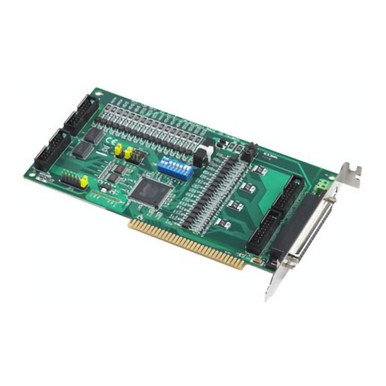
The PCL-730 card has one function switch and four jumper settings. The following sections tell how to configure the card. You may want to refer to the opposite page for help identifying card components. Card connector, jumper and switch locations... - Page 14 3F0. Other devices in your system may, however, be using some of these addresses. We set the PCL-730 for a base address of Hex 300 at the factory. If you need to adjust it to some other address range, set switch SW1 as...
- Page 15 Jumper JP1 controls the card's IRQ level, as shown below. Position X disables the interrupt. JP1 Interrupt level 2 3 4 5 6 7 X (default) Jumper JP2 selects the trigger edge (rising or falling) on which the card will trigger an interrupt. Jumper settings appear below: JP2 Trigger method Rising edge interrupt triggering (default) Falling edge interrupt triggering...
- Page 16 CN4 pin 1 TTL DI channel 1 CN4 pin 2 Jumper JP4 controls the pin assignments for CN1 and CN6. Setting this jumper to A1 makes the card's pin assignments the same as the A1 version. JP4 Version control PCL-730 User's Manual...
- Page 17 Save the screw to secure the interface card retaining bracket. 6. Carefully grasp the upper edge of the PCL-730 card. Align the hole in the retaining bracket with the hole on top of the expansion slot and align the gold striped edge connector with the expansion slot socket.
- Page 18 PCL-730 User's Manual...
- Page 19 Chapter 3 Signal Connections...
- Page 20 The PCL-730 has four on-board 20-pin flat-cable connectors (insula- tion displacement, mass termination) and a DB-37 connector accessi- ble from the card bracket. See the figure on page 7 for the location of each connector.
-
Page 21: Chapter 3 Signal Connections
IDO 0 IDO 1 IDO 2 IDO 3 IDO 4 IDO 5 IDO 6 IDO 7 IDO 8 9 10 IDO 9 IDO 10 11 12 IDO 11 IDO 12 13 14 IDO 13 IDO 14 15 16 IDO 15 E.GND 17 18 E.GND... - Page 22 EI.GND1 EI.GND2 *PCOM1/E.GND E.GND IDO 0 IDO 1 IDO 2 IDO 3 IDO 4 IDO 5 IDO 6 IDO 7 IDO 8 IDO 9 IDO 10 IDO 11 IDO 12 IDO 13 IDO 14 IDO 15 PCOM2 PCL-730 User's Manual...
- Page 23 The PCL-730 has 16 TTL-level digital inputs and 16 TTL-level digital outputs. The following figure shows connections to exchange digital signals with other TTL devices: PCL-730 TTL Devices D.GND D.GND If you want to receive an OPEN/SHORT signal from a switch or relay, add a pull-up resistor to ensure that the input is held at a high level when the contacts are open.
- Page 24 P C 8 1 7 C L O A D I D O N P N V D D N P N D C ( 5 - 4 0 V ) E . G N D E . G N D PCL-730 User's Manual...
-
Page 25: Appendix A Register Format
Appendix A Register Format... - Page 26 Programming the PCL-730 is extremely simple. Each I/O channel corresponds to a bit in the card's registers. To turn on an output channel you write a ‘‘1” to the corresponding bit. To read an input port, you simply read from the register.
- Page 27 Appendix B PC I/O Port Address Map...
- Page 28 378 - 37F LPT1: (1st printer port) 380 - 3AF Reserved 3B0 - 3BF Mono Display/Print adapter 3C0 - 3CF Reserved 3D0 - 3DF Color/Graphics 3E0 - 3EF Reserved 3F0 - 3F7 Floppy disk drive 3F8 - 3FF COM1: PCL-730 User's Manual...
Need help?
Do you have a question about the PCL-730 and is the answer not in the manual?
Questions and answers