
Subscribe to Our Youtube Channel
Related Manuals for Advantech PCI-1240


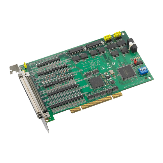
Summary of Contents for Advantech PCI-1240
- Page 1 PCI-1240 4-Axis PCI Stepping/Pulse-type Servo Motor Control Card PCI-1240U 4-Axis Universal PCI Stepping/ Pulse-type Servo Motor Control Card User Manual...
- Page 2 Acknowledgments PC-LabCard is a trademark of Advantech Co., Ltd. IBM and PC are trademarks of International Business Machines Corporation. MS-DOS, ®...
- Page 3 Product Warranty (2 years) Advantech warrants to you, the original purchaser, that each of its prod- ucts will be free from defects in materials and workmanship for two years from the date of purchase. This warranty does not apply to any products which have been repaired or...
- Page 4 Step 1. Visit the Advantech web site at www.advantech.com/support where you can find the latest information about the product. Step 2. Contact your distributor, sales representative, or Advantech's cus- tomer service center for technical support if you need additional assistance. Please have the following information ready before...
-
Page 5: Table Of Contents
Chapter 3 Signal Connections ........14 I/O Connector Pin Assignments........14 Location of Jumpers and DIP switch ......14 Figure 3.1:I/O Connector Pin Assignments for PCI-1240 & PCI-1240U 15 Table 3.1:PCI-1240/PCI-1240U I/O Connector Signal Description (part 1) 16 Table 3.1:PCI-1240/PCI-1240U I/O Connector Signal Description (part 2) 17 Table 3.1:PCI-1240/PCI-1240U I/O Connector Signal... - Page 6 3.15.4 Input Pulse Timing ............35 Figure 3.24:Timing diagram of Quadrature Pulse of En- coder Input 35 Figure 3.25:Timing diagram of UP/DOWN Pulse Input . 3.15.5 Instantaneous Stop Timing .......... 36 Figure 3.26:Timing diagram of External Instantaneous PCI-1240/PCI-1240U User Manual...
- Page 7 Table C.1:PCI-1240/PCI-1240U WRITE register func- tion 49 Table C.2:PCI-1240/PCI-1240U WRITE register format Table C.3:PCI-1240/PCI-1240U READ register function Table C.4:PCI-1240/PCI-1240U READ register format . MCX314/MCX314AS WRITE Registers: WR0 ~ WR7 53 Clear Interrupt Register: CLRINT ........53 Table C.5:Clear Interrupt Register: CLRINT - Write BASE +10 53 Pulse Generator Mode/Status Register: PGM/PGSTA ...
- Page 8 Figure E.1:Wiring Diagram with Mitsubishi MR-J2S Se- ries Motor Driver 60 Figure E.2:Wiring Diagram with Oriental LIMO EZMC Series Motor Driver 61 Figure E.3:Wiring Diagram with Panasonic MINAS-A Series Motor Driver 62 Figure E.4:Wiring Diagram with Yaskawa SGDM Series Motor Driver 63 PCI-1240/PCI-1240U User Manual viii...
- Page 9 Introduction This chapter introduces PCI-1240 and PCI-1240U and lists their features and detailed specifications.
-
Page 10: Chapter 1 Introduction
For advanced applications, we supply Windows DLL drivers and user-friendly examples to decrease your pro- gramming load. Moreover, through a free bundled PCI-1240 motion util- ity, you can complete configuration and diagnosis easily. 1.1 Features... - Page 11 • "Go home” functions (PCI-1240U only) • Universal PCI Bus for both 3.3 and 5 V PCI slots (PCI-1240U only) The Advantech PCI-1240/PCI-1240U offers the following main features: Individual Control for 4 Axes Each of the four axes has identical function capabilities, and is controlled by the same method of operation with constant speed, trapezoidal or S-curve driving.
- Page 12 Each axis has two 32-bit compare registers for logical position counter and real position counter. The comparison result can be read from the sta- tus registers. The comparison result can be notified by an interrupt signal. These registers can be also functioned as software limits. PCI-1240/PCI-1240U User Manual...
-
Page 13: Applications
Driving by External Signal It is possible to control each axis by external signals. The +/- direction fixed pulse driving and continuous driving can be also performed through the external signals. This function is used for JOG or teaching modes, and will share the CPU load. -
Page 14: Installation Guide
1.3 Installation Guide Before you install your PCI-1240/PCI-1240U card, please make sure you have the following necessary components: • PCI-1240 or PCI-1240U DAS card • PCI-1240/PCI-1240U’s User Manual • Driver Software Advantech PCI-1240/PCI-1240U DLL drivers (Included in the com- panion CD-ROM) •... - Page 15 Installation This chapter gives users a package item checklist, proper instructions about unpacking and step-by-step procedures for both driver and card installation.
-
Page 16: Chapter 2 Installation
Chapter 2 Installation 2.1 Unpacking After receiving your PCI-1240/PCI-1240U package, please inspect its contents first. The package should contain the following items: PCI-1240/PCI-1240U card Companion CD-ROM (DLL driver included) User’s Manual The PCI-1240/PCI-1240U card harbors certain electronic components vulnerable to electrostatic discharge (ESD). ESD could easily damage the integrated circuits and certain components if preventive measures are not carefully paid attention to. -
Page 17: Driver Installation
2.2 Driver Installation We recommend you to install the driver before you install the PCI-1240/PCI-1240U card into your system, since this will guarantee a smooth installation process. The 32-bit DLL driver Setup program for the card is included on the companion CD-ROM that is shipped with your DAS card package. -
Page 18: Figure 2.1:The Setup Screen Of Advantech Automation Software
Figure 2.1: The Setup Screen of Advantech Automation Software Step 3: Select the PCI-1240/PCI-1240U DLL Drivers option. Step 4: Select the proper Windows OS option according to your operating system. Just follow the installation instructions step by step to complete your DLL driver setup. -
Page 19: Figure 2.2:Different Options For Driver Setup
Figure 2.2: Different options for Driver Setup Step 5: Then setup the PCI-1240/PCI-1240U Motion Utility automati- cally. For further information on driver-related issues, an online version of Software Manual is available by accessing the following path: Start\Advantech Automation\Motion\PCI-1240\ The example source codes could be found under the corresponding instal-... -
Page 20: Hardware Installation
Step 4: Touch the metal part on the surface of your computer to neutralize the static electricity that might be on your body. Step 5: Insert the PCI-1240/PCI-1240U card into a PCI slot. Hold the card only by its edges and carefully align it with the slot. Insert the card firmly into place. - Page 21 Signal Connections This chapter provides useful informa- tion about how to connect input and output signals to the PCI-1240/PCI- 1240U via the I/O connector.
-
Page 22: Chapter 3 Signal Connections
BoardID setting is useful for identifying each card’s unique device number. We set the BoardID switch of PCI-1240/PCI-1240U to 0 at the factory. If you need to adjust it to another number, set SW1 by referring to Table 3.3. -
Page 23: Pci-1240U
Figure 3.1: I/O Connector Pin Assignments for PCI-1240 & PCI-1240U Chapter 3... - Page 24 Table 3.1: PCI-1240/PCI-1240U I/O Connector Signal Description (part 1) Signal Name Reference Direction Description Input External Power (12~24VDC) Input Emergency Stop (for all axes) XLMT+ Input + Direction Limit at X axis XLMT- Input - Direction Limit at X axis...
-
Page 25: Description (Part 2)
Table 3.1: PCI-1240/PCI-1240U I/O Connector Signal Description (part 2) Signal Name Reference Direction Description XOUT6 Output General Output at X axis (Server on) XOUT7 Output General Output at X axis (Reset) XP+P Output Output pulse CW/Pulse+ of X-axis XP+N Output... -
Page 26: Description (Part 3)
Table 3.1: PCI-1240/PCI-1240U I/O Connector Signal Description (part 3) Signal Name Reference Direction Description UALARM Input Servo Error at U axis UECAP Input Encoder Phase A at U axis UECAN Input Encoder Phase A at U axis UECBP Input Encoder Phase B at U axis... -
Page 27: Figure 3.2:Location Of Jumpers And Dip Switch On Pci 1240/Pci-1240U
Figure 3.2: Location of Jumpers and DIP switch on PCI-1240/PCI-1240U Table 3.2: BoardID register Board ID register Base Add.+12h Abbreviation BDID3 BDID2 BDID1 BDID ID0: the least significant bit (LSB) of Board ID ID3: the most significant bit (MSB) of Board ID Table 3.3: BoardID setting... -
Page 28: Output Pulse Definition (Np+P, Np+N, Np-P, Np-N)
3.3 Output Pulse Definition (nP+P, nP+N, nP-P, nP-N) The output pulse command of PCI-1240/PCI-1240U is from MCX314/ MCX314AS chip. The pulse command has two types. One is in Up/Down mode and another is in Pulse/Direction mode. While nP+P is differential from nP+N and nP-P is differential from nP-N. -
Page 29: Figure 3.4:Photo Coupler Input Interface
The following figure 3-4 and 3-5 show the examples of input circuitry connection for both photo coupler and motor driver respectively. Figure 3.4: Photo Coupler Input Interface Figure 3.5: Line Driver Input Interface Chapter 3... -
Page 30: General Purposed Output (Nout7 ~ Nout4)
VEX DC12~24V will source the photo cou- pler, and then the nLMTP in MCX314/MCX314AS will be low level. This enables the over traveling function if the desired level of nLMTP is set to low. Figure 3.7: Circuit Diagram for Movement Limit Input Signals PCI-1240/PCI-1240U User Manual... -
Page 31: Figure 3.8:Example Of Photo Sensor Used In The Limit Input Signal
The response time of this circuit should take about 0.2 ~ 0.4 msec because of the delay of photo coupled and RC filter. The following figure 3-8 is an example of photo sensor used in the case of over traveling limit switch input. -
Page 32: Figure 3.10:Input Signal For Servo Motor
When servo drives have an abnormal condition, they active this signal to note PCI-1240/PCI-1240U to stop output pulses. When enable the nALARM function of PCI-1240/PCI-1240U, the D14 bit of RR2 will set to 1 after nALARM active. If PCI-1240/PCI-1240U is driving pulses out- put, the output pulses will stop immediately when nALARM active. -
Page 33: Figure 3.11:Circuit Diagram Of Encoder Feedback
Figure 3.11: Circuit Diagram of Encoder Feedback From the circuit diagram above, PCI-1240/PCI-1240U use high speed photo coupler for isolation. The encoder output can be differential mode or open-collector mode. When n***P is high and n***N is low, the real feedback signal (n***) to MCX314/MCX314AS is low. -
Page 34: Figure 3.12:Example Of Connection Diagram For Differ Ential-Output Line Driver
Figure 3.12: Example of Connection Diagram for Differential-output Line Driver The following figure is an example of connection for the encoder with open-collector output. Figure 3.13: Example of Connection for Open Collector Output Encoder PCI-1240/PCI-1240U User Manual... -
Page 35: External Pulse Control Input (Nexop+, Nexop-)
3.9 External Pulse Control Input (nEXOP+, nEXOP-) The pulses output function of MCX314/MCX314AS chip is controlled by register setting or by external pulse command input (nEXOP+, nEXOP-). There are two output pulse mode for the external control pin. One is fixed pulse output mode, and the other is continuous output mode. -
Page 36: Emergency Stop Input (Emg)
3.11 External Power Input (VEX) External power is necessary for all input signals of each axis. Please apply DC12~24V voltage as your need. Current consumption of each point for input signal is DC12V = 3.3 mA, DC24V = 7 mA. PCI-1240/PCI-1240U User Manual... -
Page 37: Interrupt Setting
When the interrupt occurs from MCX314/MCX314AS, the interrupt sig- nal of MCX314/MCX314AS will be changed from high to low. Because the PCI bus interrupt is high level sensitive, the PCI-1240/PCI-1240U inverse the signal and latch the signal to adapt the PCI bus INTA. The Fig- 3.17 shows the interrupt structure of the PCI-1240/PCI-1240U. -
Page 38: Connection Examples For Motor Drivers
3.13 Connection Examples for Motor Drivers 3.13.1 Connection to Step Motor Drivers The following figure is an example of PCI-1240/PCI-1240U connected to 5-phase micro-step motor drives, KR515M manufactured by TECHNO company. Figure 3.18: Example of Connecting to KR515M Drive Note... - Page 39 The following figure is an example of PCI-1240/PCI-1240U connected to UPK step drive manufactured by ORIENTAL company. Figure 3.19: Example of Connecting to UPK Step Drive Note The differential pulse output of PCI-1240/PCI- 1240U is connected to CW/CCW input of UPK drive.
-
Page 40: Connection To Servo Motor Drivers
3.13.2 Connection to Servo Motor Drivers The figure shown below is an example of PCI-1240/PCI-1240U con- nected to MINAS X series AC servo motor drive. Figure 3.20: Example of MINAS X series AC servo Motor Drive Note The servo drive must be set in pulse-control drive mode and the type of pulse input is CW/CCW mode. -
Page 41: Field Wiring Considerations
3.14 Field Wiring Considerations When you use the PCI-1240/PCI-1240U to acquire data from outside, noises in the environment might significantly affect the accuracy of your measurements if due cautions are not taken. The following measures will helpful to reduce possible interference running signal wires between sig- nal sources and the PCI-1240/PCI-1240U. -
Page 42: I/O Signal Timing
• Output pulses (nP ± P, nP ± N) for drive control and general purpose output signals (nOUT4 ~ 7) for I/O control will be determined after 250 nsec from power on reset. • User can access PCI-1240/PCI-1240U only after 500 nsec from power- on reset. 3.15.2 Individual Axis Driving Figure 3.22: Timing diagram of Individual Axis Driving... -
Page 43: Interpolation Driving
3.15.3 Interpolation Driving Figure 3.23: Timing diagram of Interpolation Driving • After interpolation command is enable, the first pulse will be outputted in 775 nsec. • If using pulse/direction mode, direction signal (nP-P) is valid in ± 125 nsec of high-level pulse signal. 3.15.4 Input Pulse Timing Quadrature Pulse of Encoder Input Figure 3.24: Timing diagram of Quadrature Pulse of Encoder Input... -
Page 44: Instantaneous Stop Timing
µ SEC + 2 pulses will be output, and then stopped. Deceleration/Stop Instruction Figure 3.29: Timing diagram of Deceleration/Stop Instruction • When the Deceleration/Stop instruction is issued during driving, at most two pulses will be output, and then stopped. PCI-1240/PCI-1240U User Manual... -
Page 45: Table 3.6:Jumper Settings Of Jp10
(PCI-1240U only) This is a special design for the customers who can use the position com- pare output to synchronize with other vision devices. For PCI-1240, the position compare output channels are nOUT4 and nOUT5, and it is open- collector type output. In which the nOUT4 and nOUT5 represent the different direction of position compare separately. - Page 46 PCI-1240/PCI-1240U User Manual...
- Page 47 Specifications...
-
Page 48: (Pci-1240U Only)37
Drive Speed 1 PPS ~ 4 MPPS (Can be changed during driving) Number of Output Fixed pulse driving Pulses PCI-1240: 0 ~ 268,435,455 PCI-1240U: 0 ~ 4,294,067,295 Pulse Output Type Pulse/Direction (1-pulse, 1-direction type) or Up/Down (2-pulse type) Output Signal... -
Page 49: Digital Input/Output
A.2 Digital Input/Output Input Signals Over Travel- nLMT+ and nLMT- ing Limit Switch Input* External nIN1 ~ 3 Deceleration/ Instantaneous Stop Signal Input Signal for nALARM (servo alarm); nINPOS (position Servo Motor command completed) Drives* Emergency EMG - one emergency stop input Stop Max. -
Page 50: Input Pulse For Encoder Interface
Cycle Max. Input Frequency 1 MHz Input Voltage 2 V DC max. High Min.: PCI-1240: 10 V DC PCI-1240U: 5 V DC Max. 30 V DC Protection 2,500 V DC Isolation Protection A.4 External Signals Driving Input Signal nEXOP+, nEXPO- Max. -
Page 51: Other Functions
A.5 Other Functions Position Range of Command -2,147,438,648 ~ Counter Position Counter (for +2,147,438,647 output pulse) Range of Actual Posi- -2,147,438,648 ~ tion Counter (for input +2,147,438,647 pulse) Comparison COMP+ Register Range -2,147,438,648 ~ Register +2,147,438,647 COMP- Register Range -2,147,438,648 ~ +2,147,438,647 Can be used for software over traveling limit Interrupt Func-... - Page 52 PCI-1240/PCI-1240U User Manual...
- Page 53 Block Diagram...
-
Page 54: Appendix B Block Diagram
Appendix B Block Diagram PCI-1240/PCI-1240U User Manual... - Page 55 Register Structure and Format...
-
Page 56: Appendix C Register Structure And Format
Appendix C Register Structure and Format C.1 Overview The PCI-1240/PCI-1240U is delivered with an easy-to-use 32-bit DLL driver for user programming under Windows operating system. We advise users to program the PCI-1240/PCI-1240U using 32-bit DLL driver provided by Advantech to avoid the complexity of low-level programming by register. -
Page 57: Tion
Table C.1: PCI-1240/PCI-1240U WRITE register function Write Address (Hex.) Symbol Register Name Content Command Register Settings for axis assignment and command XWR1 X Axis Mode Register 1 Enable/disable deceleration and set YWR1 Y Axis Mode Register 1 deceleration level. Z Axis Mode Register 1 ZWR1 Enable/disable interrupt for each axis. - Page 58 Table C.2: PCI-1240/PCI-1240U WRITE register format Base Add. D15 D14 D13 D12 D11 D10 D9 Command Register: WR0 RESET Axis Assignments Command Code Mode Register 1: WR1 ≥ ≥ D-END C-STA C-END P C+ P < C+ P < C- P...
- Page 59 Table C.3: PCI-1240/PCI-1240U READ register function Read Address (Hex.) Symbol Register Name Content Limit switch status, driving status, ready Main status register for interpolation, quadrant for circle interpolation, and the stack of BP XRR1 X Axis Status Register 1 YRR1...
- Page 60 Table C.4: PCI-1240/PCI-1240U READ register format Base Add. 15 Main Status Register: RR0 BPSC1 BPSC0 ZONE2 ZONE1ZONE0CNEXT I-DRV U-ERR Z-ERR Y-ERR X-ERR U-DRV Z-DRV Y-DRV Z-DRV Error Status of Each Axis Driving Status of Each Axis Status Register 1: RR1...
-
Page 61: Mcx314/Mcx314As Write Registers: Wr0 ~ Wr7
C.3 MCX314/MCX314AS WRITE Registers: WR0 ~ WR7 The PCI-1240/PCI-1240U registers from WR0 (Base Add. + 0) to WR7 (Base Add. + E) are the same as mapping registers on MCX314/ MCX314AS chip, and please refer to MCX314/MCX314AS user’s man- ual Section 4.3 ~ Section 4.9 for detailed information. -
Page 62: Pgmsta - Write/Read Base +14
A/B phase pulse input The following table indicates the external signal routing path. The external signals generate the pulses to drive the motor are connected to the pins nEXOP+ and nEXOP- (Please refer to the pin assignment). PCI-1240/PCI-1240U User Manual... -
Page 63: Mcx314/Mcx314As Read Registers: Rr0 ~ Rr7
U-axis C.6 MCX314/MCX314AS READ Registers: RR0 ~ RR7 The PCI-1240/PCI-1240U registers from RR0 (Base Add. + 0) to RR7 (Base Add. + E) are the same as mapping registers on MCX314/ MCX314AS chip, and please refer to MCX314/MCX314AS user’s man- ual Section 4.10 ~ Section 4.15 for detailed information. -
Page 64: Interrupt Status Register: Intsta
This bit indicates whether interrupt occurred or not. 1 means that an interrupt has occurred. C.8 Board ID Register: BDID BDID shows the Board ID of the PCI-1240/PCI-1240U. Table C.11: Board ID Register: BDID - Read BASE +12 Base Add. 15... - Page 65 Cable Pin Assignments...
-
Page 66: Appendix D Cable Pin Assignments
Appendix D Cable Pin Assignments PCI-1240/PCI-1240U User Manual... - Page 67 Wiring with Third-Party Motor Drivers...
-
Page 68: Appendix E Wiring With Third-Party Motor Drivers
Appendix E Wiring with Third-Party Motor Drivers Figure E.1: Wiring Diagram with Mitsubishi MR-J2S Series Motor Driver PCI-1240/PCI-1240U User Manual... -
Page 69: Figure E.2:Wiring Diagram With Oriental Limo Ezmc Series Motor Driver
Figure E.2: Wiring Diagram with Oriental LIMO EZMC Series Motor Driver Chapter E... -
Page 70: Figure E.3:Wiring Diagram With Panasonic Minas-A Series Motor Driver
Figure E.3: Wiring Diagram with Panasonic MINAS-A Series Motor Driver PCI-1240/PCI-1240U User Manual... -
Page 71: Figure E.4:Wiring Diagram With Yaskawa Sgdm Series Motor Driver
Figure E.4: Wiring Diagram with Yaskawa SGDM Series Motor Driver Chapter E... - Page 72 PCI-1240/PCI-1240U User Manual...
Need help?
Do you have a question about the PCI-1240 and is the answer not in the manual?
Questions and answers