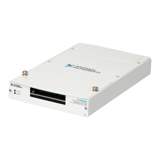
National Instruments M Series User Manual

National Instruments M Series User Manual

Multifunction i/o modules and devices
Hide thumbs Also See for M Series:
Table of Contents

Advertisement

National Instruments M Series User Manual

Advertisement

Table of Contents
loading

Summary of Contents for National Instruments M Series

  • Page 1 Artisan Technology Group is your source for quality new and certified-used/pre-owned equipment SERVICE CENTER REPAIRS WE BUY USED EQUIPMENT • FAST SHIPPING AND DELIVERY Experienced engineers and technicians on staff Sell your excess, underutilized, and idle used equipment at our full-service, in-house repair center We also offer credit for buy-backs and trade-ins •...
  • Page 2 DAQ M Series M Series User Manual NI 622x, NI 625x, and NI 628x Multifunction I/O Modules and Devices M Series User Manual July 2016 371022L-01 Artisan Technology Group - Quality Instrumentation ... Guaranteed | (888) 88-SOURCE | www.artisantg.com...
  • Page 3 For further support information, refer to the appendix. To comment on NI documentation, refer to the NI website at and enter the Info Code ni.com/info feedback © 2004–2016 National Instruments. All rights reserved. Artisan Technology Group - Quality Instrumentation ... Guaranteed | (888) 88-SOURCE | www.artisantg.com...
  • Page 4 National Instruments Corporation. National Instruments respects the intellectual property of others, and we ask our users to do the same. NI software is protected by copyright and other intellectual property laws. Where NI software may be used to reproduce software or other materials belonging to others, you may use NI software only to reproduce materials that you may reproduce in accordance with the terms of any applicable license or other legal restriction.
  • Page 5 ™ The ExpressCard word mark and logos are owned by PCMCIA and any use of such marks by National Instruments is under license. The mark LabWindows is used under a license from Microsoft Corporation. Windows is a registered trademark of Microsoft Corporation in the United States and other countries.
  • Page 6: Table Of Contents

    Installation ........................1-3 Unpacking......................... 1-3 Device Self-Calibration ....................1-4 Getting Started with M Series PCI Express Devices and the Disk Drive Power Connector ........................1-5 When to Use the Disk Drive Power Connector ............1-5 Disk Drive Power Connector Installation..............1-5 Getting Started with M Series USB Devices..............
  • Page 7 Contents 37-Pin M Series Cables and Accessories..............2-8 37-Pin Cables....................2-9 37-Pin Screw Terminal Accessories ..............2-9 RTSI Cables ...................... 2-9 37-Pin Custom Cabling..................2-9 Signal Conditioning ......................2-10 Sensors and Transducers...................2-10 Signal Conditioning Options ..................2-10 SCXI ......................... 2-10 SCC........................
  • Page 8 M Series User Manual Connecting Ground-Referenced Signal Sources .............. 4-17 What Are Ground-Referenced Signal Sources? ............4-17 When to Use Differential Connections with Ground-Referenced Signal Sources ........................4-18 When to Use Non-Referenced Single-Ended (NRSE) Connections with Ground-Referenced Signal Sources ..............4-18 When to Use Referenced Single-Ended (RSE) Connections with Ground-Referenced Signal Sources ..............
  • Page 9 Contents Chapter 5 Analog Output AO Offset and AO Reference Selection ................5-2 Minimizing Glitches on the Output Signal ...............5-3 Analog Output Data Generation Methods ................ 5-3 Software-Timed Generations ..................5-3 Hardware-Timed Generations................... 5-4 Analog Output Triggering ....................5-5 Connecting Analog Output Signals .................. 5-5 Analog Output Timing Signals ..................
  • Page 10 M Series User Manual Connecting Digital I/O Signals..................6-8 Getting Started with DIO Applications in Software............6-9 Chapter 7 Counters Counter Input Applications ....................7-1 Counting Edges......................7-2 Single Point (On-Demand) Edge Counting ............7-2 Buffered (Sample Clock) Edge Counting............7-3 Controlling the Direction of Counting..............
  • Page 11 Contents Counter Timing Signals ....................7-24 Counter n Source Signal ...................7-24 Routing a Signal to Counter n Source .............. 7-25 Routing Counter n Source to an Output Terminal ..........7-25 Counter n Gate Signal....................7-25 Routing a Signal to Counter n Gate ..............7-26 Routing Counter n Gate to an Output Terminal ..........
  • Page 12 M Series User Manual Chapter 9 Digital Routing and Clock Generation Clock Routing........................9-1 80 MHz Timebase ....................9-2 20 MHz Timebase ....................9-2 100 kHz Timebase ....................9-2 External Reference Clock..................9-2 10 MHz Reference Clock ..................9-2 Synchronizing Multiple Devices ..................9-3 PXI/PXI Express Modules..................
  • Page 13 NI 6284 ..........................A-61 NI 6289 ..........................A-63 Appendix B Timing Diagrams Appendix C Troubleshooting Appendix D Upgrading from E Series to M Series Appendix E Where to Go from Here Appendix F NI Services Index xii | ni.com Artisan Technology Group - Quality Instrumentation ... Guaranteed | (888) 88-SOURCE | www.artisantg.com...
  • Page 14 M Series User Manual Figures Figure A-1. PCI/PXI-6220 Pinout ................A-2 Figure A-2. PCI/PXI-6221 Pinout ................A-5 Figure A-3. USB-6221 Screw Terminal Pinout............A-7 Figure A-4. USB-6221 BNC Top Panel and Pinout ..........A-9 Figure A-5. PCI-6221 (37-Pin) Pinout..............A-11 Figure A-6.
  • Page 15: Getting Started

    M Series device. Safety Guidelines Operate the NI 62xx M Series devices and modules only as described in this user manual. NI 62xx devices and modules are not certified for use in hazardous Caution locations.
  • Page 16: Safety Guidelines For Hazardous Voltages

    Chapter 1 Getting Started Safety Guidelines for Hazardous Voltages If hazardous voltages are connected to the device/module, take the following precautions. A hazardous voltage is a voltage greater than 42.4 V or 60 VDC to earth ground. Caution Ensure that hazardous voltage wiring is performed only by qualified personnel adhering to local electrical standards.
  • Page 17: Hardware Symbol Definitions

    Unpacking The M Series device ships in an antistatic package to prevent electrostatic discharge (ESD). ESD can damage several components on the device. Never touch the exposed pins of connectors.
  • Page 18: Device Self-Calibration

    Store the device in the antistatic package when the device is not in use. Device Self-Calibration NI recommends that you self-calibrate your M Series device after installation and whenever the ambient temperature changes. Self-calibration should be performed after the device has warmed up for the recommended time period.
  • Page 19: Getting Started With M Series Pci Express Devices And The Disk Drive Power Connector

    Disk Drive Power Connector Installation Before installing the disk drive power connector, you must install and set up the M Series PCI Express device as described in the DAQ Getting Started Guide for PCI/PCI Express. Complete the following steps to install the disk drive power connector.
  • Page 20: Getting Started With M Series Usb Devices

    Device Self-Calibration described in the section. Getting Started with M Series USB Devices The following sections contain information about M Series USB device features and best practices. Applying the Signal Label to USB Screw Terminal Devices The supplied signal label can be adhered to...
  • Page 21 M Series User Manual You can attach a wire to the ground lug screw of any USB-62xx device, as shown in Figure 1-3. Figure 1-3. Grounding a USB-62xx Device through the Ground Lug Screw NATIONAL NI USB-62xx INSTRUMENTS Multifunction I/O with...
  • Page 22: Usb Device Panel/Wall Mounting

    LED Patterns Connector (USB-622 /625 /628 Devices) Refer to the section of Chapter 3, and LED Information, for information about the M Series USB device LEDs. USB Cable Strain Relief (USB-622 /625 /628 Screw Terminal and USB-622 /625 /628 Mass Termination Devices) Use the supplied strain relief hardware to provide strain relief for your USB cable.
  • Page 23: Usb Device Fuse Replacement

    Signal Wire Strain Relief Security Cable Slot USB Device Fuse Replacement M Series USB devices have a replaceable T 2A 250V (5 × 20 mm) fuse that protects the device from overcurrent through the power connector. (USB-6281/6289 Devices) USB-628x devices also have a replaceable Littelfuse 0453002 (F 2A 250V) fuse that protects the device from overcurrent through the +5 V terminal(s).
  • Page 24 Chapter 1 Getting Started Figure 1-8. USB-62xx Screw Terminal Fuse Locations T 2A 250V (5 × 20 mm) Fuse Littelfuse 0453002 Fuse on USB-628x Devices Replace the lid and screws. (USB-622 /625 BNC Devices) To replace a broken fuse in the USB-62xx BNC, complete the following steps.
  • Page 25 M Series User Manual Figure 1-9. USB-62xx BNC Fuse Location T 2A 250V (5 × 20 mm) Fuse Remove both end pieces by unscrewing the four sockethead cap screws with a 7/64 in. hex wrench. Note The end pieces are attached using self-threading screws. Repeated screwing and unscrewing of self-threading screws will produce a compromised connection.
  • Page 26: Usb Device Security Cable Slot

    Chapter 1 Getting Started (USB-622 /625 /628 Mass Termination Devices) To replace a broken fuse in the USB-62xx Mass Termination, complete the following steps. Power down and unplug the device. Remove the USB cable and signal cable(s) from the device. Loosen the four Phillips screws that attach the lid to the enclosure and remove the lid.
  • Page 27: Installing A Ferrite

    Module/Device-Specific Information, for M Series device pinouts. Refer to Appendix A, Specifications Refer to the device specifications document for your device. M Series device documentation is available on ni.com/manuals Accessories and Cables NI offers a variety of accessories and cables to use with your multifunction I/O DAQ module...
  • Page 28: Daq System Overview

    DAQ System Overview Figure 2-1 shows a typical DAQ system, which includes sensors, transducers, signal conditioning devices, cables that connect the various devices to the accessories, the M Series device, programming software, and PC. The following sections cover the components of a typical DAQ system.
  • Page 29: Daq-Stc2 And Daq-6202

    Independent scatter-gather DMA controllers for all acquisition and generation functions Calibration Circuitry The M Series analog inputs and outputs have calibration circuitry to correct gain and offset errors. You can calibrate the device to minimize AI and AO errors caused by time and temperature drift at run time.
  • Page 30: Cables And Accessories

    M Series User Manual Cables and Accessories NI offers a variety of products to use with M Series PCI, PCI Express, PXI, PXI Express, USB devices, including cables, connector blocks, and other accessories, as follows: • Shielded cables and cable assemblies, and unshielded ribbon cables and cable assemblies •...
  • Page 31 Chapter 2 DAQ System Overview Table 2-1. 68-Pin M Series Device/Module Cables and Accessories PCI, PCI Express, PXI, PXI Express Devices and Modules USB Mass Termination Devices 622x/625x/ 628x 622x/625x/ Connector 0 628x Connector 0 6224/6229/ 6254/6259/ 6229/6259/ Cables and Accessories...
  • Page 32: 68-Pin Cables

    Cabling options differ between the 68-pin PCI/PCI Express/PXI/PXI Express devices and modules and USB Mass Termination devices. PCI/PCI Express/PXI/PXI Express Device/Module 68-Pin Cables You can use the following cables with PCI, PCI Express, PXI, and PXI Express M Series devices and modules: SHC68-68-EPM •...
  • Page 33: 68-Pin Bnc Accessories

    SCB-68A, SCB-68—Shielded connector block with temperature sensor • TB-2706 • —Front panel mounted terminal block for PXI/PXI Express M Series devices SCC-68—I/O connector block with screw terminals, general breadboard area, bus • terminals, and four expansion slots for SCC signal conditioning modules.
  • Page 34: Scxi

    To connect your M Series device or module to an SCXI chassis, use the SCXI-1349 adapter and your 68-pin cable. Use Connector 0 of your M Series device to control SCXI in parallel and multiplexed mode. Use Connector 1 of your M Series device to control SCXI in parallel mode.
  • Page 35: Usb Device Accessories, Usb Cable, And Power Supply

    However, NI offers a variety of products to use with the USB M Series devices, as shown in Table 2-2. Table 2-2. USB Device Cabling, Accessories, and Power Supply...
  • Page 36: 37-Pin Cables

    R37F-37M—37-pin female-to-male ribbon I/O cable • 37-Pin Screw Terminal Accessories National Instruments offers several styles of screw terminal connector blocks. Use your 37-pin cable to connect a PCI-6221 (37-pin) device to one of the following connector blocks: CB-37F-HVD—37-pin DIN rail screw terminal block •...
  • Page 37: Signal Conditioning

    SCXI is a front-end signal conditioning and switching system for various measurement devices, including M Series devices. An SCXI system consists of a rugged chassis that houses shielded signal conditioning modules that amplify, filter, isolate, and multiplex analog signals from thermocouples or other transducers.
  • Page 38: Scc

    Note Screw Terminal, or USB-622x/625x BNC devices. SCC is a front-end signal conditioning system for M Series plug-in data acquisition devices. An SCC system consists of a shielded carrier that holds up to 20 single- or dual-channel SCC modules for conditioning thermocouples and other transducers. SCC is designed for small measurement systems where you need only a few channels of each signal type, or for portable applications.
  • Page 39 Chapter 2 DAQ System Overview M Series devices use the NI-DAQmx driver. NI-DAQmx includes a collection of programming examples to help you get started developing an application. You can modify example code and save it in an application. You can use examples to develop a new application or add example code to an existing application.
  • Page 40: Connector And Led Information

    Descriptions, +5 V Power Source, and USER 1 and USER 2 sections contain information about M Series connector signals, power, and user-defined terminals. The LED Patterns section contains information about M Series USB device LEDs. Module/Device-Specific Information, for device I/O...
  • Page 41 Chapter 3 Connector and LED Information Table 3-1. I/O Connector Signals Signal Name Reference Direction Description Analog Input Ground—These terminals are the AI GND — — reference point for single-ended AI measurements in RSE mode and the bias current return point for DIFF measurements.
  • Page 42: Power Source

    M Series User Manual Table 3-1. I/O Connector Signals (Continued) Signal Name Reference Direction Description Digital Ground—D GND supplies the reference D GND — — for P0.<0..31>, PFI <0..15>/P1/P2, and +5 V. All three ground references—AI GND, AO GND, and D GND—are connected on the device. Refer...
  • Page 43: User 1 And User 2

    Chapter 6, PFI. Refer to Table 7-6, 68-Pin Device Default NI-DAQmx Counter/Timer Pins, to find the default NI-DAQmx counter/timer pins for most M Series devices. User-Defined Channels—On USB-62xx BNC USER <1,2> — — devices, the USER <1,2> BNC connectors allow you to use a BNC connector for a digital or timing I/O signal of your choice.
  • Page 44 Never connect the +5 V power terminals to analog or digital ground or to Caution any other voltage source on the M Series device or any other device. Doing so can damage the device and the computer. NI is not liable for damage resulting from such a connection.
  • Page 45 Chapter 3 Connector and LED Information Figure 3-1. USER 1 and USER 2 BNC Connections USER 1 BNC USER 2 BNC D GND D GND USER 1 Internal Connection USER 2 D GND +5 V D GND P0.0 P0.1 Screw P0.2 Terminal P0.3...
  • Page 46: Rtsi Connector Pinout

    /628 Devices) All variants of M Series USB devices have LEDs labeled ACTIVE and READY. The ACTIVE LED indicates activity over the bus. The READY LED indicates whether or not the device is configured. Table 3-2 shows the behavior of the LEDs.
  • Page 47: Analog Input

    M Series devices use the NI-PGIA to deliver high accuracy even when sampling multiple channels with small input ranges at fast rates. M Series devices can sample channels in any order at the maximum conversion rate, and you can individually program each channel in a sample with a different input range.
  • Page 48: Analog Input Range

    You can individually program the input range of each AI channel on your M Series device. The input range affects the resolution of the M Series device for an AI channel. Resolution refers to the voltage of one ADC code. For example, a 16-bit ADC converts analog inputs into one of 65,536 (= 2 ) codes—that is, one of 65,536 possible digital values.
  • Page 49: Analog Input Lowpass Filter

    M Series User Manual Table 4-1 shows the input ranges and resolutions supported by each M Series device family. Table 4-1. M Series Input Range and Nominal Resolution Nominal Resolution Assuming M Series Devices Input Range 5% Over Range NI 622x -10 V to 10 V 320 µV...
  • Page 50: Analog Input Ground-Reference Settings

    Chapter 2, Analog Input Ground-Reference Settings M Series devices support the analog input ground-reference settings: Differential mode—In DIFF mode, the M Series device measures the difference in voltage • between two AI signals. Referenced single-ended mode—In RSE mode, the M Series device measures the voltage •...
  • Page 51 M Series User Manual Figure 4-2. NI-PGIA Instrumentation Amplifier PGIA Measured in– Voltage – ] × Gain = [V – V in– Table 4-2 shows how signals are routed to the NI-PGIA. Table 4-2. Signals Routed to the NI-PGIA Signals Routed to the...
  • Page 52: Configuring Ai Ground-Reference Settings In Software

    In multichannel scanning applications, accuracy is affected by settling time. When your M Series device switches from one AI channel to another AI channel, the device configures the NI-PGIA with the input range of the new channel. The NI-PGIA then amplifies the input signal with the gain for the new input range.
  • Page 53 The capacitance of the cable also can increase the settling time. National Instruments recommends using individually shielded, twisted-pair wires that are Connecting Analog Input 2 m or less to connect AI signals to the device. Refer to the Signals section for more information.
  • Page 54 Chapter 4 Analog Input Consider again the example above where a 4 V signal is connected to channel 0 and a 1 mV signal is connected to channel 1. Suppose the input range for channel 0 is -10 V to 10 V and the input range of channel 1 is -200 mV to 200 mV. You can connect channel 2 to AI GND (or you can use the internal ground;...
  • Page 55: Analog Input Data Acquisition Methods

    M Series User Manual Analog Input Data Acquisition Methods When performing analog input measurements, you either can perform software-timed or hardware-timed acquisitions. Software-Timed Acquisitions With a software-timed acquisition, software controls the rate of the acquisition. Software sends a separate command to the hardware to initiate each ADC conversion. In NI-DAQmx, software-timed acquisitions are referred to as having on-demand timing.
  • Page 56: Analog Input Triggering

    Refer to the sections for information about these triggers. An analog or digital trigger can initiate these actions. All M Series devices support digital triggering, but some do not support analog triggering. To find your device triggering options, refer to the specifications document for your device.
  • Page 57: Connecting Analog Input Signals

    M Series User Manual Connecting Analog Input Signals Table 4-3 summarizes the recommended input configuration for both types of signal sources. Table 4-3. Analog Input Configuration Floating Signal Sources (Not Connected to Ground-Referenced † Building Ground) Signal Sources Examples: Example: •...
  • Page 58: Connecting Floating Signal Sources

    Chapter 4 Analog Input Connecting Floating Signal Sources What Are Floating Signal Sources? A floating signal source is not connected to the building ground system, but has an isolated ground-reference point. Some examples of floating signal sources are outputs of transformers, thermocouples, battery-powered devices, optical isolators, and isolation amplifiers.
  • Page 59: When To Use Referenced Single-Ended (Rse) Connections With Floating Signal Sources

    M Series User Manual With this type of connection, the NI-PGIA rejects both the common-mode noise in the signal and the ground potential difference between the signal source and the device ground. Using Non-Referenced Single-Ended (NRSE) Connections for Floating Signal...
  • Page 60 Chapter 4 Analog Input Figure 4-4. Differential Connections for Floating Signal Sources without Bias Resistors M Series Device Floating Signal Source – AI– Impedance AI SENSE <100 Ω AI GND However, for larger source impedances, this connection leaves the DIFF signal path significantly off balance.
  • Page 61 AI GND I/O Connector M Series Module/Device Configured in Differential Mode Both inputs of the NI-PGIA require a DC path to ground in order for the NI-PGIA to work. If the source is AC coupled (capacitively coupled), the NI-PGIA needs a resistor between the positive input and AI GND.
  • Page 62: Using Non-Referenced Single-Ended (Nrse) Connections For Floating Signal Sources

    Chapter 4 Analog Input Figure 4-7. Differential Connections for AC Coupled Floating Sources with Balanced Bias Resistors M Series Device AC Coupling AC Coupled Floating Signal Source – AI– AI SENSE AI GND Using Non-Referenced Single-Ended (NRSE) Connections for Floating Signal Sources It is important to connect the negative lead of a floating signals source to AI GND (either directly or through a resistor).
  • Page 63: Using Referenced Single-Ended (Rse) Connections For Floating Signal Sources

    M Series User Manual Using Referenced Single-Ended (RSE) Connections for Floating Signal Sources Figure 4-9 shows how to connect a floating signal source to the M Series device configured for RSE mode. Figure 4-9. RSE Connections for Floating Signal Sources AI <0..n>...
  • Page 64: When To Use Differential Connections With Ground-Referenced Signal Sources

    Chapter 4 Analog Input When to Use Differential Connections with Ground-Referenced Signal Sources Use DIFF input connections for any channel that meets any of the following conditions: • The input signal is low level (less than 1 V). • The leads connecting the signal to the device are greater than 3 m (10 ft). •...
  • Page 65: When To Use Referenced Single-Ended (Rse) Connections With Ground-Referenced Signal Sources

    AI GND and the ground of the sensor. In RSE mode, this ground loop causes measurement errors. Using Differential Connections for Ground-Referenced Signal Sources Figure 4-10 shows how to connect a ground-referenced signal source to the M Series device configured in DIFF mode. Figure 4-10. Differential Connections for Ground-Referenced Signal Sources AI +...
  • Page 66: Using Non-Referenced Single-Ended (Nrse) Connections For Ground-Referenced Signal Sources

    Noise – and Ground Potential M Series Device Configured in NRSE Mode Note (NI USB-62xx BNC Devices) To measure a ground-referenced signal source on USB BNC devices, move the switch under the BNC connector to the GS position. AI+ and AI- must both remain within ±11 V of AI GND.
  • Page 67: Field Wiring Considerations

    Info Code ni.com/info rdfwn3 Analog Input Timing Signals In order to provide all of the timing functionality described throughout this section, M Series devices have a flexible timing engine. Figure 4-12 summarizes all of the timing options provided Clock Routing Digital by the analog input timing engine.
  • Page 68 The sampling rate is the fastest you can acquire data on the device and still achieve accurate results. For example, if an M Series device has a sampling rate of 250 kS/s, this sampling rate is aggregate—one channel at 250 kS/s or two channels at 125 kS/s per channel illustrates the relationship.
  • Page 69: Ai Sample Clock Signal

    Use the AI Sample Clock (ai/SampleClock) signal to initiate a set of measurements. Your M Series device samples the AI signals of every channel in the task once for every AI Sample Clock. A measurement acquisition consists of one or more samples.
  • Page 70: Using An Internal Source

    Chapter 4 Analog Input Using an Internal Source One of the following internal signals can drive AI Sample Clock: Counter n Internal Output • • AI Sample Clock Timebase (divided down) • A pulse initiated by host software A programmable internal counter divides down the sample clock timebase. Several other internal signals can be routed to AI Sample Clock through RTSI.
  • Page 71: Ai Sample Clock Timebase Signal

    M Series User Manual Figure 4-16 shows the relationship of AI Sample Clock to AI Start Trigger. Figure 4-16. AI Sample Clock and AI Start Trigger AI Sample Clock Timebase AI Start Trigger AI Sample Clock Delay From Start Trigger...
  • Page 72: Using An Internal Source

    Chapter 4 Analog Input NI-DAQmx chooses the fastest conversion rate possible based on the speed of the A/D converter and adds 10 μs of padding between each channel to allow for adequate settling time. This scheme enables the channels to approximate simultaneous sampling and still allow for adequate settling time.
  • Page 73: Using A Delay From Sample Clock To Convert Clock

    Clock Other Timing Requirements The sample and conversion level timing of M Series devices work such that clock signals are gated off unless the proper timing requirements are met. For example, the device ignores both AI Sample Clock and AI Convert Clock until it receives a valid AI Start Trigger signal. Once the device recognizes an AI Sample Clock pulse, it ignores subsequent AI Sample Clock pulses until it receives the correct number of AI Convert Clock pulses.
  • Page 74 Chapter 4 Analog Input Figure 4-19. AI Convert Clock Too Fast For AI Sample Clock; AI Convert Clock Pulses Are Gated Off AI Sample Clock AI Convert Clock Channel Measured 1 2 3 1 2 3 1 2 3 Sample #1 Sample #2 Sample #3 Figure 4-20.
  • Page 75: Ai Convert Clock Timebase Signal

    M Series User Manual AI Convert Clock Timebase Signal The AI Convert Clock Timebase (ai/ConvertClockTimebase) signal is divided down to provide one of the possible sources for AI Convert Clock. Use one of the following signals as the source of AI Convert Clock Timebase: •...
  • Page 76: Using An Analog Source

    Chapter 4 Analog Input The source also can be one of several other internal signals on your DAQ device. Refer to Device Routing in MAX in the NI-DAQmx Help or the LabVIEW Help for more information. You also can specify whether the measurement acquisition begins on the rising edge or falling edge of AI Start Trigger.
  • Page 77: Using A Digital Source

    M Series User Manual When the reference trigger occurs, the DAQ device continues to write samples to the buffer until the buffer contains the number of posttrigger samples desired. Figure 4-23 shows the final buffer. Figure 4-23. Reference Trigger Final Buffer...
  • Page 78: Using A Digital Source

    Note Pause triggers are only sensitive to the level of the source, not the edge. Getting Started with AI Applications in Software You can use the M Series device in the following analog input applications: • Single-point analog input •...
  • Page 79: Analog Output

    • first-in-first-out (FIFO) memory buffer between the computer and the DACs. It allows you to download the points of a waveform to your M Series device without host computer interaction. AO Sample Clock—The AO Sample Clock signal reads a sample from the DAC FIFO and •...
  • Page 80: Ao Offset And Ao Reference Selection

    Chapter 5 Analog Output AO Offset and AO Reference Selection AO offset and AO reference selection allow you to set the AO range. The AO range describes the set of voltages the device can generate. The digital codes of the DAC are spread evenly across the AO range.
  • Page 81: Minimizing Glitches On The Output Signal

    M Series User Manual On NI 628x devices, the AO reference of each analog output can be individually set to one of the following: – ±10 V – ±5 V – ±APFI <0,1> – ±AO <0..3> You can connect an external signal to APFI <0,1> to provide the AO reference.
  • Page 82: Hardware-Timed Generations

    Chapter 5 Analog Output Hardware-Timed Generations With a hardware-timed generation, a digital hardware signal controls the rate of the generation. This signal can be generated internally on your device or provided externally. Hardware-timed generations have several advantages over software-timed acquisitions: •...
  • Page 83: Analog Output Triggering

    Start trigger • Pause trigger An analog or digital trigger can initiate these actions. All M Series devices support digital triggering, but some do not support analog triggering. To find your device’s triggering options, AO Start Trigger Signal refer to the specifications document for your device. Refer to the AO Pause Trigger Signal sections for more information about these triggering actions.
  • Page 84: Analog Output Timing Signals

    Timebase Programmable 20 MHz Timebase Clock Divider 100 kHz Timebase PXI_CLK10 M Series devices feature the following AO (waveform generation) timing signals: AO Start Trigger Signal • AO Pause Trigger Signal • AO Sample Clock Signal • AO Sample Clock Timebase Signal •...
  • Page 85: Using An Analog Source

    M Series User Manual You also can specify whether the waveform generation begins on the rising edge or falling edge of AO Start Trigger. Using an Analog Source When you use an analog trigger source, the waveform generation begins on the first rising edge Triggering with an Analog Source of the Analog Comparison Event signal.
  • Page 86: Using A Digital Source

    Chapter 5 Analog Output Using a Digital Source To use AO Pause Trigger, specify a source and a polarity. The source can be one of the following signals: • PFI <0..15> • RTSI <0..7> • PXI_STAR The source also can be one of several other internal signals on your DAQ device. Refer to Device Routing in MAX in the NI-DAQmx Help or the LabVIEW Help for more information.
  • Page 87: Routing Ao Sample Clock Signal To An Output Terminal

    M Series User Manual Routing AO Sample Clock Signal to an Output Terminal You can route AO Sample Clock (as an active low signal) out to any PFI <0..15> or RTSI <0..7> terminal. Other Timing Requirements A counter on your device internally generates AO Sample Clock unless you select some external source.
  • Page 88: Getting Started With Ao Applications In Software

    AO Sample Clock rather than AO Sample Clock Timebase. Getting Started with AO Applications in Software You can use an M Series device in the following analog output applications: • Single-point (on-demand) generation •...
  • Page 89: Digital I/O

    Digital I/O M Series devices contain up to 32 lines of bidirectional DIO signals on Port 0. In addition, M Series devices have up to 16 PFI signals that can function as static DIO signals. M Series devices support the following DIO features on Port 0: •...
  • Page 90: Static Dio

    Static DIO Each of the M Series DIO lines can be used as a static DI or DO line. You can use static DIO lines to monitor or control digital signals. Each DIO can be individually configured as a digital input (DI) or digital output (DO).
  • Page 91: Digital Waveform Acquisition

    Use the DI Sample Clock (di/SampleClock) signal to sample the P0.<0..31> terminals and store the result in the DI waveform acquisition FIFO. M Series devices do not have the ability to divide down a timebase to produce an internal DI Sample Clock for digital waveform acquisition.
  • Page 92: Using An External Source

    Use the DO Sample Clock (do/SampleClock) signal to update the DO terminals with the next sample from the DO waveform generation FIFO. M Series devices do not have the ability to divide down a timebase to produce an internal DO Sample Clock for digital waveform generation.
  • Page 93: Using An Internal Source

    M Series User Manual Using an Internal Source To use DO Sample Clock with an internal source, specify the signal source and the polarity of the signal. The source can be any of the following signals: • AI Sample Clock (ai/SampleClock) •...
  • Page 94: Programmable Power-Up States

    NI-DAQmx or MAX. Note When using your M Series device to control an SCXI chassis, DIO lines 0, 1, 2, and 4 are used as communication lines and must be left to power-up in the default high-impedance state to avoid potential damage to these signals.
  • Page 95: Di Change Detection

    M Series User Manual DI Change Detection You can configure the DAQ device to detect changes in the DIO signals. Figure 6-3 shows a block diagram of the DIO change detection circuitry. Figure 6-3. DI Change Detection Enable P0.0 Synch...
  • Page 96: Di Change Detection Applications

    Exceeding the maximum input voltage ratings, which are listed in the Caution specifications document for each M Series device, can damage the DAQ device and the computer. NI is not liable for any damage resulting from such signal connections. 6-8 | ni.com...
  • Page 97: Getting Started With Dio Applications In Software

    M Series User Manual Getting Started with DIO Applications in Software You can use the M Series device in the following digital I/O applications: • Static digital input • Static digital output • Digital waveform generation • Digital waveform acquisition •...
  • Page 98: Counter Input Applications

    The counters have seven input signals, although in most applications only a few inputs are used. Default Counter/Timer Pinouts For information about connecting counter signals, refer to the section. Counter Input Applications The following sections list the various counter input applications available on M Series devices: Counting Edges • Pulse-Width Measurement •...
  • Page 99: Counting Edges

    (up or down) as described in the Counting section. Us the following edge counting options to read the counter values on your M Series device: Single Point (On-Demand) Edge Counting • Buffered (Sample Clock) Edge Counting •...
  • Page 100: Buffered (Sample Clock) Edge Counting

    M Series User Manual Buffered (Sample Clock) Edge Counting With buffered edge counting (edge counting using a sample clock), the counter counts the number of edges on the Source input after the counter is armed. The value of the counter is sampled on each active edge of a sample clock.
  • Page 101: Single Pulse-Width Measurement

    If a counter is armed while the pulse is in the active state, it will wait for the next transition to the active state to begin the measurement. Refer to the following sections for more information about M Series pulse-width measurement options: Single Pulse-Width Measurement •...
  • Page 102: Period Measurement

    You can calculate the period of the Gate input by multiplying the period of the Source signal by the number of edges returned by the counter. Refer to the following sections for more information about M Series period measurement options: Single Period Measurement •...
  • Page 103: Buffered Period Measurement

    Chapter 7 Counters Figure 7-7 shows an example of a single period measurement. Figure 7-7. Single Period Measurement GATE SOURCE Counter Value HW Save Register Buffered Period Measurement Buffered period measurement is similar to single period measurement, but buffered period measurement measures multiple periods.
  • Page 104: Semi-Period Measurement

    You can calculate the semi-period of the Gate input by multiplying the period of the Source signal by the number of edges returned by the counter. Refer to the following sections for more information about M Series semi-period measurement options: Single Semi-Period Measurement •...
  • Page 105: Frequency Measurement

    Chapter 7 Counters Note that if you are using an external signal as the Source, at least one Source pulse should occur between each active edge of the Gate signal. This condition ensures that correct values are returned by the counter. If this condition is not met, consider using duplicate count prevention, Duplicate Count Prevention described in the section.
  • Page 106: Low Frequency With One Counter (Averaged)

    M Series User Manual Low Frequency with One Counter (Averaged) In this method, you measure several periods of your signal using a known timebase. This method is good for low to medium frequency signals. You can route the signal to measure (F1) to the Gate of a counter. You can route a known timebase (Ft) to the Source of the counter.
  • Page 107: Large Range Of Frequencies With Two Counters

    You then measure the long pulse with a known timebase. The M Series device can measure this long pulse more accurately than the faster input signal. You can route the signal to measure to the Source input of Counter 0, as shown in Figure 7-13.
  • Page 108: Choosing A Method For Measuring Frequency

    M Series User Manual Then, route the Counter 0 Internal Output signal to the Gate input of Counter 1. You can route a signal of known frequency (F2) to the Counter 1 Source input. F2 can be 80MHzTimebase. For signals that might be slower than 0.02 Hz, use a slower known timebase. Configure Counter 1 to perform a single pulse-width measurement.
  • Page 109 Chapter 7 Counters Table 7-1. Frequency Measurement Methods One Counter Two Counters High Variable — Averaged Frequency Large Range Known Known timebase Known timebase ------------------------------- timebase gating period --- - ------------ - --- - gating period Maximum × × × -------------- - ------------------------ - ------------------------ -...
  • Page 110 M Series User Manual Table 7-2. 50 kHz Frequency Measurement Methods (Continued) One Counter Two Counters High Variable — Averaged Frequency Large Range Maximum 1,000 frequency error (Hz) Maximum error 0.05 0.001 0.001 From these results, you can see that while the measurement time for one counter is shorter, the accuracy is best in the sample clocked and two counter large range measurements.
  • Page 111: Position Measurement

    Chapter 7 Counters bandwidth; if such bandwidth is not available due to other measurements taking place, this method may fail to transfer all the required samples to perform the measurement. • Using two counters for high frequency measurements is accurate for high frequency signals.
  • Page 112: Measurements Using Quadrature Encoders

    M Series User Manual Refer to the following sections for more information about the M Series position measurement options: Measurements Using Quadrature Encoders • Measurements Using Two Pulse Encoders • Buffered (Sample Clock) Position Measurement • Measurements Using Quadrature Encoders The counters can perform measurements of quadrature encoders that use X1, X2, or X4 encoding.
  • Page 113: Measurements Using Two Pulse Encoders

    Chapter 7 Counters Channel Z Behavior Some quadrature encoders have a third channel, channel Z, which is also referred to as the index channel. A high level on channel Z causes the counter to be reloaded with a specified value in a specified phase of the quadrature cycle.
  • Page 114: Buffered (Sample Clock) Position Measurement

    M Series User Manual Buffered (Sample Clock) Position Measurement With buffered position measurement (position measurement using a sample clock), the counter increments based on the encoding used after the counter is armed. The value of the counter is sampled on each active edge of a sample clock. A DMA controller transfers the sampled values to host memory.
  • Page 115: Single Two-Signal Edge-Separation Measurement

    Chapter 7 Counters Refer to the following sections for more information about the M Series edge-separation measurement options: Single Two-Signal Edge-Separation Measurement • Buffered Two-Signal Edge-Separation Measurement • Single Two-Signal Edge-Separation Measurement With single two-signal edge-separation measurement, the counter counts the number of rising (or falling) edges on the Source input occurring between an active edge of the Gate signal and an active edge of the Aux signal.
  • Page 116: Counter Output Applications

    • Frequency Division • Pulse Generation for ETS • Simple Pulse Generation Refer to the following sections for more information about the M Series simple pulse generation options: Single Pulse Generation • Single Pulse Generation with Start Trigger • Retriggerable Single Pulse Generation •...
  • Page 117: Single Pulse Generation With Start Trigger

    Chapter 7 Counters Single Pulse Generation with Start Trigger The counter can output a single pulse in response to one pulse on a hardware Start Trigger signal. The pulse appears on the Counter n Internal Output signal of the counter. You can route the Start Trigger signal to the Gate input of the counter.
  • Page 118: Pulse Train Generation

    M Series User Manual Pulse Train Generation Refer to the following sections for more information about the M Series pulse train generation options: Continuous Pulse Train Generation • Finite Pulse Train Generation • Continuous Pulse Train Generation This function generates a train of pulses with programmable frequency and duty cycle. The pulses appear on the Counter n Internal Output signal of the counter.
  • Page 119: Finite Pulse Train Generation

    Using the Frequency Generator The frequency generator can output a square wave at many different frequencies. The frequency generator is independent of the two general-purpose 32-bit counter/timer modules on M Series devices. Figure 7-27 shows a block diagram of the frequency generator.
  • Page 120: Frequency Division

    M Series User Manual Figure 7-28 shows the output waveform of the frequency generator when the divider is set to 5. Figure 7-28. Frequency Generator Output Waveform Frequency Output Timebase FREQ OUT (Divisor = 5) Frequency Output can be routed out to any PFI <0..15> or RTSI <0..7> terminal. All PFI terminals are set to high-impedance at startup.
  • Page 121: Counter Timing Signals

    D3 = D1 + 2ΔD Default Counter/Timer Pinouts For information about connecting counter signals, refer to the section. Counter Timing Signals M Series devices feature the following counter timing signals: Counter n Source Signal • Counter n Gate Signal •...
  • Page 122: Routing A Signal To Counter N Source

    M Series User Manual Table 7-5. Counter Applications and Counter n Source Application Purpose of Source Terminal Pulse Generation Counter Timebase One Counter Time Measurements Counter Timebase Two Counter Time Measurements Input Terminal Non-Buffered Edge Counting Input Terminal Buffered Edge Counting...
  • Page 123: Routing A Signal To Counter N Gate

    Chapter 7 Counters Routing a Signal to Counter n Gate Each counter has independent input selectors for the Counter n Gate signal. Any of the following signals can be routed to the Counter n Gate input: • RTSI <0..7> • PFI <0..15>...
  • Page 124: Counter N A, Counter N B, And Counter N Z Signals

    M Series User Manual In addition, Counter 1 Internal Output, Counter 1 Gate, Counter 1 Source, or Counter 0 Gate can be routed to Counter 0 Aux. Counter 0 Internal Output, Counter 0 Gate, Counter 0 Source, or Counter 1 Gate can be routed to Counter 1 Aux.
  • Page 125: Counter N Internal Output And Counter N Tc Signals

    Chapter 7 Counters • AI Reference Trigger (ai/ReferenceTrigger) • AI Start Trigger (ai/StartTrigger) • PXI_STAR • Analog Comparison Event Counter 1 Internal Output can be routed to Counter 0 HW Arm. Counter 0 Internal Output can be routed to Counter 1 HW Arm. Some of these options may not be available in some driver software.
  • Page 126: Counter Triggering

    NI-DAQmx. Refer to Connecting Counter Signals in the NI-DAQmx Help or the LabVIEW Help for more information about how to connect your signals for common counter measurements and generations. M Series default PFI lines for counter functions are listed in Physical Channels in the NI-DAQmx Help or the LabVIEW Help.
  • Page 127: Other Counter Features

    When the filters are enabled, your device samples the input on each rising edge of a filter clock. M Series devices use an onboard oscillator to generate the filter clock with a 40 MHz frequency. NI-DAQmx only supports filters on counter inputs.
  • Page 128 When a PFI input is routed directly to RTSI, or a RTSI input is routed directly to PFI, the M Series device does not use the filtered version of the input signal. Refer to the KnowledgeBase document, Digital Filtering with M Series and CompactDAQ, for more information about digital filters and counters.
  • Page 129: Prescaling

    Prescaling allows the counter to count a signal that is faster than the maximum timebase of the counter. M Series devices offer 8X and 2X prescaling on each counter (prescaling can be disabled). Each prescaler consists of a small, simple counter that counts to eight (or two) and rolls over.
  • Page 130: Example Application That Works Correctly (No Duplicate Counting)

    M Series User Manual Example Application That Works Correctly (No Duplicate Counting) Figure 7-32 shows an external buffered signal as the period measurement Source. Figure 7-32. Duplicate Count Prevention Example Rising Edge of Gate Counter detects rising edge of Gate on the next rising edge of Source.
  • Page 131: Example Application That Prevents Duplicate Count

    Chapter 7 Counters Example Application That Prevents Duplicate Count With duplicate count prevention enabled, the counter synchronizes both the Source and Gate signals to the 80 MHz Timebase. By synchronizing to the timebase, the counter detects edges on the Gate even if the Source does not pulse. This enables the correct current count to be stored in the buffer even if no Source edges occur between Gate signals, as shown in Figure 7-34.
  • Page 132: Enabling Duplicate Count Prevention In Ni-Daqmx

    Synchronization Modes The 32-bit counter counts up or down synchronously with the Source signal. The Gate signal and other counter inputs are asynchronous to the Source signal. So M Series devices synchronize these signals before presenting them to the internal counter.
  • Page 133: 80 Mhz Source Mode

    Chapter 7 Counters 80 MHz Source Mode In 80 MHz source mode, the device synchronizes signals on the rising edge of the source, and counts on the following rising edge of the source, as shown in Figure 7-35. Figure 7-35. 80 MHz Source Mode Source Synchronize Count...
  • Page 134: Pfi

    M Series devices have up to 16 Programmable Function Interface (PFI) signals. In addition, M Series devices have up to 32 lines of bidirectional DIO signals. Each PFI can be individually configured as the following: • A static digital input •...
  • Page 135: Using Pfi Terminals As Timing Input Signals

    The voltage input and output levels and the current drive levels of the PFI signals are listed in the specifications of your device. Using PFI Terminals as Timing Input Signals Use PFI terminals to route external timing signals to many different M Series functions. Each PFI terminal can be routed to any of the following signals: •...
  • Page 136: Using Pfi Terminals As Static Digital I/Os

    /P1.x or PFI x/P2.x. each terminal is labeled PFI In addition, M Series devices have up to 32 lines of bidirectional DIO signals. Connecting PFI Input Signals All PFI input connections are referenced to D GND. Figure 8-2 shows this reference, and how to connect an external PFI 0 source and an external PFI 2 source to two PFI terminals.
  • Page 137: Pfi Filters

    When the filters are enabled, your device samples the input on each rising edge of a filter clock. M Series devices use an onboard oscillator to generate the filter clock with a 40 MHz frequency. NI-DAQmx only supports filters on counter inputs.
  • Page 138: I/O Protection

    NI-DAQmx or MAX. Note When using your M Series device to control an SCXI chassis, DIO lines 0, 1, 2, and 4 are used as communication lines and must be left to power-up in the default high-impedance state to avoid potential damage to these signals.
  • Page 139: Clock Routing

    – User input through the PXI_STAR terminal • Routes and generates the main clock signals for the M Series device. Clock Routing Figure 9-1 shows the clock routing circuitry of an M Series device. Figure 9-1. M Series Clock Routing Circuitry...
  • Page 140: 80 Mhz Timebase

    10 MHz Reference Clock The 10 MHz reference clock can be used to synchronize other devices to your M Series device. The 10 MHz reference clock can be routed to the RTSI <0..7> terminals. Other devices connected to the RTSI bus can use this signal as a clock input.
  • Page 141: Synchronizing Multiple Devices

    USB Devices With the PFI bus and the routing capabilities of USB M Series devices, there are several ways to synchronize multiple devices depending on your application. To synchronize multiple devices to a common timebase, choose one device—the initiator—to generate the timebase.
  • Page 142: Real-Time System Integration (Rtsi)

    Use a common clock (or timebase) to drive the timing engine on multiple devices • Share trigger signals between devices Many National Instruments DAQ, Motion, Vision, and CAN devices support RTSI. RTSI is not supported on USB devices. Note In a PCI/PCI Express system, the RTSI bus consists of the RTSI bus interface and a ribbon cable.
  • Page 143: Using Rtsi As Outputs

    M Series User Manual Table 9-1. RTSI Signals RTSI Bus Signal Terminal RTSI 7 RTSI 6 RTSI 5 RTSI 4 RTSI 3 RTSI 2 RTSI 1 RTSI 0 Not Connected. Do not connect signals to these terminals. 1 to 18...
  • Page 144: Using Rtsi Terminals As Timing Input Signals

    When the filters are enabled, your device samples the input on each rising edge of a filter clock. M Series devices use an onboard oscillator to generate the filter clock with a 40 MHz frequency. NI-DAQmx only supports filters on counter inputs.
  • Page 145 When a PFI input is routed directly to RTSI, or a RTSI input is routed directly to PFI, the M Series device does not use the filtered version of the input signal. Refer to the KnowledgeBase document, Digital Filtering with M Series and CompactDAQ, for more information about digital filters and counters.
  • Page 146: Pxi Clock And Trigger Signals

    PXI_STAR can be used as an external source for many AI, AO, and counter signals. An M Series device is not a Star Trigger controller. An M Series device may be used in the first peripheral slot of a PXI system, but the system will not be able to use the Star Trigger feature.
  • Page 147 When a PFI input is routed directly to RTSI, or a RTSI input is routed directly to PFI, the M Series device does not use the filtered version of the input signal. Refer to the KnowledgeBase document, Digital Filtering with M Series and CompactDAQ, for more information about digital filters and counters.
  • Page 148: Bus Interface

    Bus Interface The bus interface circuitry of M Series devices efficiently moves data between host memory and the measurement and acquisition circuits. M Series devices are available for the following platforms: • • PCI Express • • PXI Express •...
  • Page 149: Usb Device Data Transfer Methods

    Output, for more information. Note On PCI, PCI Express, PXI, and PXI Express M Series devices, each measurement and acquisition circuit (that is, AI, AO, and so on) has a dedicated DMA channel. So in most applications, all data transfers use DMA. However, NI-DAQmx allows you to disable DMA and use interrupts.
  • Page 150: Pxi Considerations

    PXI and PXI Express NI PXI M Series devices can be installed in any PXI chassis and most slots of PXI Express hybrid chassis. NI PXI Express M Series devices can be installed in any PXI Express slot in PXI Express chassis.
  • Page 151: Using Pxi With Compactpci

    For some PXI M Series devices, there are two variants—one that will work in PXI hybrid slots and one that supports local bus for SCXI control when the device is in the right-most slot. Refer to the device specifications for more information.
  • Page 152: Triggering

    When you configure a trigger, you must decide how you want to produce the trigger and the action you want the trigger to cause. All M Series devices support internal software triggering, as well as external digital triggering. Some devices also support analog triggering. For...
  • Page 153: Triggering With An Analog Source

    Chapter 11 Triggering Triggering with an Analog Source Some M Series devices can generate a trigger on an analog signal. To find your device triggering options, refer to the specifications document for your device. Figure 11-2 shows the analog trigger circuit.
  • Page 154: Analog Trigger Actions

    M Series User Manual This behavior places some restrictions on using AI channels as trigger sources. When you use an analog start trigger, the trigger channel must be the first channel in the channel list. When you use an analog reference or pause trigger, and the analog channel is the source of the trigger, there can be only one channel in the channel list.
  • Page 155 Chapter 11 Triggering In above-level analog triggering mode, shown in Figure 11-4, the trigger is generated when the signal value is greater than Level. Figure 11-4. Above-Level Analog Triggering Mode Level Analog Comparison Event Analog Edge Triggering with Hysteresis—Hysteresis adds a programmable voltage •...
  • Page 156 M Series User Manual – Analog Edge Trigger with Hysteresis (Falling Slope)—When using hysteresis with a falling slope, you specify a trigger level and amount of hysteresis. The low threshold is the trigger level; the high threshold is the trigger level plus the hysteresis.
  • Page 157: Analog Trigger Accuracy

    Chapter 11 Triggering Analog Trigger Accuracy The analog trigger circuitry compares the voltage of the trigger source to the output of programmable trigger DACs. When you configure the level (or the high and low limits in window trigger mode), the device adjusts the output of the trigger DACs. Refer to the specifications document for your device to find the accuracy or resolution of these DACs, which also shows the accuracy or resolution of analog triggers.
  • Page 158 Module/Device-Specific Information This appendix contains device pinouts, and information about specifications, cable and accessory choices, and other important topics for the following M Series modules/devices: NI 6220 • NI 6221 (68-Pin) • NI PCI-6221 (37-Pin) • NI 6224 • NI 6225 •...
  • Page 159: Figure A-1. Pci/Pxi-6220 Pinout

    Appendix A Module/Device-Specific Information NI 6220 PCI/PXI-6220 Pinout Figure A-1 shows the pinout of the PCI/PXI-6220. Figure A-1. PCI/PXI-6220 Pinout 68 34 AI 0 (AI 0+) AI 8 (AI 0-) 67 33 AI GND AI 1 (AI 1+) 66 32 AI 9 (AI 1-) AI GND AI 2 (AI 2+)
  • Page 160 The following list contains links specific to your DAQ device: Specifications—Refer to the NI 6220 Specifications for more detailed information about • the PCI/PXI-6220 device. Accessory and Cabling Options—Refer to the 68-Pin M Series Cables and Accessories • DAQ System Overview, for more information. section of Chapter 2, ©...
  • Page 161: Ni 6221 (68-Pin)

    Appendix A Module/Device-Specific Information NI 6221 (68-Pin) The following sections contain information about the PCI/PXI-6221, USB-6221 Screw Terminal, and USB-6221 BNC. PCI/PXI-6221 PCI/PXI-6221 Pinout Figure A-2 shows the pinout of the PCI/PXI-6221. A-4 | ni.com Artisan Technology Group - Quality Instrumentation ... Guaranteed | (888) 88-SOURCE | www.artisantg.com...
  • Page 162: Figure A-2. Pci/Pxi-6221 Pinout

    M Series User Manual Figure A-2. PCI/PXI-6221 Pinout 68 34 AI 0 (AI 0+) AI 8 (AI 0-) 67 33 AI GND AI 1 (AI 1+) 66 32 AI 9 (AI 1-) AI GND 65 31 AI 2 (AI 2+)
  • Page 163 The following list contains links specific to your DAQ device: Specifications—Refer to the NI 6221 Specifications for more detailed information about • the PCI/PXI-6221 device. Accessory and Cabling Options—Refer to the 68-Pin M Series Cables and Accessories • DAQ System Overview, for more information. section of Chapter 2, A-6 | ni.com...
  • Page 164: Figure A-3. Usb-6221 Screw Terminal Pinout

    M Series User Manual USB-6221 Screw Terminal USB-6221 Screw Terminal Pinout Figure A-3 shows the pinout of the USB-6221 Screw Terminal. Figure A-3. USB-6221 Screw Terminal Pinout AI 4 (AI 4+) PFI 8/P2.0 AI 0 (AI 0+) P0.0 AI 12 (AI 4-)
  • Page 165 Appendix A Module/Device-Specific Information Table A-3. Default NI-DAQmx Counter/Timer Pins (Continued) Counter/Timer Signal Default Pin Number (Name) CTR 1 SRC 76 (PFI 3) CTR 1 GATE 77 (PFI 4) CTR 1 AUX 87 (PFI 11) CTR 1 OUT 91 (PFI 13) CTR 1 A 76 (PFI 3) CTR 1 Z...
  • Page 166: Figure A-4. Usb-6221 Bnc Top Panel And Pinout

    M Series User Manual USB-6221 BNC USB-6221 BNC Pinout Figure A-4 shows the pinout of the USB-6221 BNC. Figure A-4. USB-6221 BNC Top Panel and Pinout © National Instruments | A-9 Artisan Technology Group - Quality Instrumentation ... Guaranteed | (888) 88-SOURCE | www.artisantg.com...
  • Page 167 Appendix A Module/Device-Specific Information Table A-4. Default NI-DAQmx Counter/Timer Pins Counter/Timer Signal Default Pin Name CTR 0 SRC PFI 8 CTR 0 GATE PFI 9 CTR 0 AUX PFI 10 CTR 0 OUT PFI 12 CTR 0 A PFI 8 CTR 0 Z PFI 9 CTR 0 B...
  • Page 168: Figure A-5. Pci-6221 (37-Pin) Pinout

    M Series User Manual NI PCI-6221 (37-Pin) PCI-6221 (37-Pin) Pinout Figure A-5 shows the pinout of the PCI-6221 (37-pin). Figure A-5. PCI-6221 (37-Pin) Pinout AI 0 (AI 0+) AI 8 (AI 0-) AI 9 (AI 1-) AI 1 (AI 1+)
  • Page 169 Specifications—Refer to the NI 6221 (37-Pin) Specifications for more detailed • information about the PCI-6221 (37-pin) device. Accessory and Cabling Options—Refer to the 37-Pin M Series Cables and Accessories • DAQ System Overview, for more information. section of Chapter 2, A-12 | ni.com...
  • Page 170: Figure A-6. Pci/Pxi-6224 Pinout

    M Series User Manual NI 6224 PCI/PXI-6224 Pinout Figure A-6 shows the pinout of the PCI/PXI-6224. The I/O signals appear on two 68-pin connectors. Figure A-6. PCI/PXI-6224 Pinout AI 0 (AI 0+) 68 34 AI 8 (AI 0-) P0.30 D GND...
  • Page 171 The following list contains links specific to your DAQ device: Specifications—Refer to the NI 6224 Specifications for more detailed information about • the PCI/PXI-6224 device. Accessory and Cabling Options—Refer to the 68-Pin M Series Cables and Accessories • DAQ System Overview, for more information. section of Chapter 2, A-14 | ni.com...
  • Page 172: Figure A-7. Pci/Pxi-6225 Pinout

    M Series User Manual NI 6225 The following sections contain information about the PCI/PXI-6225, USB-6225 Screw Terminal, and USB-6225 Mass Termination. PCI/PXI-6225 PCI/PXI-6225 Pinout Figure A-7 shows the pinout of the PCI/PXI-6225. Figure A-7. PCI/PXI-6225 Pinout AI 0 (AI 0+)
  • Page 173 The following list contains links specific to your DAQ device: Specifications—Refer to the NI 6225 Specifications for more detailed information about • the PCI/PXI-6225 device. Accessory and Cabling Options—Refer to the 68-Pin M Series Cables and Accessories • DAQ System Overview, for more information. section of Chapter 2, A-16 | ni.com...
  • Page 174: Figure A-8. Usb-6225 Screw Terminal Pinout

    M Series User Manual USB-6225 Screw Terminal USB-6225 Screw Terminal Pinout Figure A-8 shows the pinout of the USB-6225 Screw Terminal. Figure A-8. USB-6225 Screw Terminal Pinout AI 8 (AI 0-) AI 27 (AI 19-) AI 0 (AI 0+) AI 19 (AI 19+)
  • Page 175 Appendix A Module/Device-Specific Information Table A-8. Default NI-DAQmx Counter/Timer Pins Counter/Timer Signal Default Pin Number (Name) CTR 0 SRC 113 (PFI 8) CTR 0 GATE 115 (PFI 9) CTR 0 AUX 117 (PFI 10) CTR 0 OUT 121 (PFI 12) CTR 0 A 113 (PFI 8) CTR 0 Z...
  • Page 176: Figure A-9. Usb-6225 Mass Termination Pinout

    M Series User Manual USB-6225 Mass Termination USB-6225 Mass Termination Pinout Figure A-9 shows the pinout of the USB-6225 Mass Termination device. Figure A-9. USB-6225 Mass Termination Pinout CONNECTOR 0 (AI 0-15) CONNECTOR 1 (AI 16-79) AI 8 (AI 0-)
  • Page 177 Chapter 1, Getting Started, for information about replacing the fuse on the USB-6225 Mass Termination. Accessory and Cabling Options—Refer to the 68-Pin M Series Cables and Accessories • DAQ System Overview, for more information. section of Chapter 2, A-20 | ni.com...
  • Page 178: Figure A-10. Pci/Pxi-6229 Pinout

    M Series User Manual NI 6229 The following sections contain information about the PCI/PXI-6229, USB-6229 Screw Terminal, and USB-6229 BNC. PCI/PXI-6229 PCI/PXI-6229 Pinout Figure A-10 shows the pinout of the PCI/PXI-6229. The I/O signals appear on two 68-pin connectors. Figure A-10. PCI/PXI-6229 Pinout...
  • Page 179 The following list contains links specific to your DAQ device: Specifications—Refer to the NI 6229 Specifications for more detailed information about • the PCI/PXI-6229 device. Accessory and Cabling Options—Refer to the 68-Pin M Series Cables and Accessories • DAQ System Overview, for more information. section of Chapter 2, A-22 | ni.com...
  • Page 180: Figure A-11. Usb-6229 Screw Terminal Pinout

    M Series User Manual USB-6229 Screw Terminal USB-6229 Screw Terminal Pinout Figure A-11 shows the pinout of the USB-6229 Screw Terminal. Figure A-11. USB-6229 Screw Terminal Pinout AI 4 (AI 4+) AI 20 (AI 20+) AI 0 (AI 0+) AI 16 (AI 16+)
  • Page 181 Appendix A Module/Device-Specific Information Table A-11. Default NI-DAQmx Counter/Timer Pins Counter/Timer Signal Default Pin Number (Name) CTR 0 SRC 81 (PFI 8) CTR 0 GATE 83 (PFI 9) CTR 0 AUX 85 (PFI 10) CTR 0 OUT 89 (PFI 12) CTR 0 A 81 (PFI 8) CTR 0 Z...
  • Page 182: Figure A-12. Usb-6229 Bnc Top Panel And Pinout

    M Series User Manual USB-6229 BNC USB-6229 BNC Pinout Figure A-12 shows the pinout of the USB-6229 BNC. Figure A-12. USB-6229 BNC Top Panel and Pinout © National Instruments | A-25 Artisan Technology Group - Quality Instrumentation ... Guaranteed | (888) 88-SOURCE | www.artisantg.com...
  • Page 183 Appendix A Module/Device-Specific Information Table A-12. Default NI-DAQmx Counter/Timer Pins Counter/Timer Signal Default Pin Name CTR 0 SRC PFI 8 CTR 0 GATE PFI 9 CTR 0 AUX PFI 10 CTR 0 OUT PFI 12 CTR 0 A PFI 8 CTR 0 Z PFI 9 CTR 0 B...
  • Page 184: Figure A-13. Pci/Pxi-6250 Pinout

    M Series User Manual NI 6250 PCI/PXI-6250 Pinout Figure A-13 shows the pinout of the PCI/PXI-6250. Figure A-13. PCI/PXI-6250 Pinout 68 34 AI 0 (AI 0+) AI 8 (AI 0-) 67 33 AI GND AI 1 (AI 1+) 66 32...
  • Page 185 The following list contains links specific to your DAQ device: Specifications—Refer to the NI 6250 Specifications for more detailed information about • the PCI/PXI-6250 device. Accessory and Cabling Options—Refer to the 68-Pin M Series Cables and Accessories • DAQ System Overview, for more information. section of Chapter 2, A-28 | ni.com...
  • Page 186: Figure A-14. Ni Pci/Pcie/Pxi/Pxie-6251 Pinout

    M Series User Manual NI 6251 PCI/PCIe/PXI/PXIe-6251, USB-6251 The following sections contain information about the Screw Terminal, USB-6251 BNC, and USB-6251 Mass Termination. NI PCI/PCIe/PXI/PXIe-6251 NI PCI/PCIe/PXI/PXIe-6251 Pinout Figure A-14 shows the pinout of the NI PCI/PCIe/PXI/PXIe-6251. Figure A-14. NI PCI/PCIe/PXI/PXIe-6251 Pinout...
  • Page 187 The following list contains links specific to your DAQ device: Specifications—Refer to the NI 6251 Specifications for more detailed information about • the NI PCI/PCIe/PXI/PXIe-6251 device. Accessory and Cabling Options—Refer to the 68-Pin M Series Cables and Accessories • DAQ System Overview, for more information. section of Chapter 2, PCI Express Disk Drive Power Connector—Refer to the...
  • Page 188: Figure A-15. Usb-6251 Screw Terminal Pinout

    M Series User Manual USB-6251 Screw Terminal USB-6251 Screw Terminal Pinout Figure A-15 shows the pinout of the USB-6251 Screw Terminal. Figure A-15. USB-6251 Screw Terminal Pinout AI 4 (AI 4+) PFI 8/P2.0 AI 0 (AI 0+) P0.0 AI 12 (AI 4-)
  • Page 189 Appendix A Module/Device-Specific Information Table A-15. Default NI-DAQmx Counter/Timer Pins (Continued) Counter/Timer Signal Default Pin Number (Name) CTR 1 GATE 77 (PFI 4) CTR 1 AUX 87 (PFI 11) CTR 1 OUT 91 (PFI 13) CTR 1 A 76 (PFI 3) CTR 1 Z 77 (PFI 4) CTR 1 B...
  • Page 190: Figure A-16. Usb-6251 Bnc Top Panel And Pinout

    M Series User Manual USB-6251 BNC USB-6251 BNC Pinout Figure A-16 shows the pinout of the USB-6251 BNC. Figure A-16. USB-6251 BNC Top Panel and Pinout © National Instruments | A-33 Artisan Technology Group - Quality Instrumentation ... Guaranteed | (888) 88-SOURCE | www.artisantg.com...
  • Page 191 Appendix A Module/Device-Specific Information Table A-16. Default NI-DAQmx Counter/Timer Pins Counter/Timer Signal Default Pin Name CTR 0 SRC PFI 8 CTR 0 GATE PFI 9 CTR 0 AUX PFI 10 CTR 0 OUT PFI 12 CTR 0 A PFI 8 CTR 0 Z PFI 9 CTR 0 B...
  • Page 192: Figure A-17. Usb-6251 Mass Termination Pinout

    M Series User Manual USB-6251 Mass Termination USB-6251 Mass Termination Pinout Figure A-17 shows the pinout of the USB-6251 Mass Termination device. Figure A-17. USB-6251 Mass Termination Pinout CONNECTOR 0 (AI 0-15) AI 0 (AI 0+) 68 34 AI 8 (AI 0-)
  • Page 193 Chapter 1, Getting Started, for information about replacing the fuse on the USB-6229 Mass Termination. Accessory and Cabling Options—Refer to the 68-Pin M Series Cables and Accessories • DAQ System Overview, for more information. section of Chapter 2, A-36 | ni.com...
  • Page 194: Figure A-18. Pci/Pxi-6254 Pinout

    M Series User Manual NI 6254 PCI/PXI-6254 Pinout Figure A-18 shows the pinout of the PCI/PXI-6254. The I/O signals appear on two 68-pin connectors. Figure A-18. PCI/PXI-6254 Pinout AI 0 (AI 0+) AI 8 (AI 0–) P0.30 D GND AI GND AI 1 (AI 1+) P0.28...
  • Page 195 The following list contains links specific to your DAQ device: Specifications—Refer to the NI 6254 Specifications for more detailed information about • the PCI/PXI-6254 device. Accessory and Cabling Options—Refer to the 68-Pin M Series Cables and Accessories • DAQ System Overview, for more information. section of Chapter 2, A-38 | ni.com...
  • Page 196: Figure A-19. Pci/Pxi-6255 Pinout

    M Series User Manual NI 6255 The following sections contain information about the PCI/PXI-6255, USB-6255 Screw Terminal, and USB-6255 Mass Termination. PCI/PXI-6255 PCI/PXI-6255 Pinout Figure A-19 shows the pinout of the PCI/PXI-6255. Figure A-19. PCI/PXI-6255 Pinout AI 0 (AI 0+) AI 8 (AI 0–)
  • Page 197 The following list contains links specific to your DAQ device: Specifications—Refer to the NI 6255 Specifications for more detailed information about • the PCI/PXI-6255 device. Accessory and Cabling Options—Refer to the 68-Pin M Series Cables and Accessories • DAQ System Overview, for more information. section of Chapter 2, A-40 | ni.com...
  • Page 198: Figure A-20. Usb-6255 Screw Terminal Pinout

    M Series User Manual USB-6255 Screw Terminal USB-6255 Screw Terminal Pinout Figure A-20 shows the pinout of the USB-6255 Screw Terminal. Figure A-20. USB-6255 Screw Terminal Pinout AI 8 (AI 0-) AI 27 (AI 19-) AI 0 (AI 0+) AI 19 (AI 19+)
  • Page 199 Appendix A Module/Device-Specific Information Table A-20. Default NI-DAQmx Counter/Timer Pins Counter/Timer Signal Default Pin Number (Name) CTR 0 SRC 113 (PFI 8) CTR 0 GATE 115 (PFI 9) CTR 0 AUX 117 (PFI 10) CTR 0 OUT 121 (PFI 12) CTR 0 A 113 (PFI 8) CTR 0 Z...
  • Page 200: Figure A-21. Usb-6255 Mass Termination Pinout

    M Series User Manual USB-6255 Mass Termination USB-6255 Mass Termination Pinout Figure A-21 shows the pinout of the USB-6255 Mass Termination device. Figure A-21. USB-6255 Mass Termination Pinout CONNECTOR 0 (AI 0-15) CONNECTOR 1 (AI 16-79) AI 16 (AI 16+)
  • Page 201 Chapter 1, Getting Started, for information about replacing the fuse on the USB-6255 Mass Termination. Accessory and Cabling Options—Refer to the 68-Pin M Series Cables and Accessories • DAQ System Overview, for more information. section of Chapter 2, A-44 | ni.com...
  • Page 202: Figure A-22. Ni Pci/Pcie/Pxi/Pxie-6259 Pinout

    M Series User Manual NI 6259 PCI/PCIe/PXI/PXIe-6259, USB-6259 The following sections contain information about the Screw Terminal, USB-6259 BNC, and USB-6259 Mass Termination. NI PCI/PCIe/PXI/PXIe-6259 NI PCI/PCIe/PXI/PXIe-6259 Pinout Figure A-22 shows the pinout of the NI PCI/PCIe/PXI/PXIe-6259. The I/O signals appear on two 68-pin connectors.
  • Page 203 The following list contains links specific to your DAQ device: Specifications—Refer to the NI 6259 Specifications for more detailed information about • the NI PCI/PCIe/PXI/PXIe-6259 device. Accessory and Cabling Options—Refer to the 68-Pin M Series Cables and Accessories • DAQ System Overview, for more information. section of Chapter 2, PCI Express Disk Drive Power Connector—Refer to the...
  • Page 204: Figure A-23. Usb-6259 Screw Terminal Pinout

    M Series User Manual USB-6259 Screw Terminal USB-6259 Screw Terminal Pinout Figure A-23 shows the pinout of the USB-6259 Screw Terminal. Figure A-23. USB-6259 Screw Terminal Pinout AI 4 (AI 4+) AI 20 (AI 20+) AI 0 (AI 0+) AI 16 (AI 16+)
  • Page 205 Appendix A Module/Device-Specific Information Table A-23. Default NI-DAQmx Counter/Timer Pins Counter/Timer Signal Default Pin Number (Name) CTR 0 SRC 81 (PFI 8) CTR 0 GATE 83 (PFI 9) CTR 0 AUX 85 (PFI 10) CTR 0 OUT 89 (PFI 12) CTR 0 A 81 (PFI 8) CTR 0 Z...
  • Page 206: Figure A-24. Usb-6259 Bnc Top Panel And Pinout

    M Series User Manual USB-6259 BNC USB-6259 BNC Pinout Figure A-24 shows the pinout of the USB-6259 BNC. Figure A-24. USB-6259 BNC Top Panel and Pinout © National Instruments | A-49 Artisan Technology Group - Quality Instrumentation ... Guaranteed | (888) 88-SOURCE | www.artisantg.com...
  • Page 207 Appendix A Module/Device-Specific Information Table A-24. Default NI-DAQmx Counter/Timer Pins Counter/Timer Signal Default Pin Name CTR 0 SRC PFI 8 CTR 0 GATE PFI 9 CTR 0 AUX PFI 10 CTR 0 OUT PFI 12 CTR 0 A PFI 8 CTR 0 Z PFI 9 CTR 0 B...
  • Page 208: Usb-6259 Mass Termination Pinout

    M Series User Manual USB-6259 Mass Termination USB-6259 Mass Termination Pinout Figure A-25 shows the pinout of the USB-6259 Mass Termination device. Figure A-25. USB-6259 Mass Termination Pinout CONNECTOR 0 (AI 0-15) CONNECTOR 1 (AI 16-31) AI 16 (AI 16+)
  • Page 209 Chapter 1, Getting Started, for information about replacing the fuse on the USB-6259 Mass Termination. Accessory and Cabling Options—Refer to the 68-Pin M Series Cables and Accessories • DAQ System Overview, for more information. section of Chapter 2, A-52 | ni.com...
  • Page 210: Pci/Pxi-6280 Pinout

    M Series User Manual NI 6280 PCI/PXI-6280 Pinout Figure A-26 shows the pinout of the PCI/PXI-6280. Figure A-26. PCI/PXI-6280 Pinout 68 34 AI 0 (AI 0+) AI 8 (AI 0-) 67 33 AI GND AI 1 (AI 1+) 66 32...
  • Page 211 The following list contains links specific to your DAQ device: Specifications—Refer to the NI 6280 Specifications for more detailed information about • the PCI/PXI-6280 device. Accessory and Cabling Options—Refer to the 68-Pin M Series Cables and Accessories • DAQ System Overview, for more information. section of Chapter 2, A-54 | ni.com...
  • Page 212: Pci/Pxi-6281 Pinout

    M Series User Manual NI 6281 The following sections contain information about the PCI/PXI-6281, USB-6281 Screw Terminal, and USB-6281 Mass Termination. PCI/PXI-6281 PCI/PXI-6281 Pinout Figure A-27 shows the pinout of the PCI/PXI-6281. Figure A-27. PCI/PXI-6281 Pinout 68 34 AI 0 (AI 0+)
  • Page 213 The following list contains links specific to your DAQ device: Specifications—Refer to the NI 6281 Specifications for more detailed information about • the PCI/PXI-6281 device. Accessory and Cabling Options—Refer to the 68-Pin M Series Cables and Accessories • DAQ System Overview, for more information. section of Chapter 2, A-56 | ni.com...
  • Page 214: Usb-6281 Screw Terminal Pinout

    M Series User Manual USB-6281 Screw Terminal USB-6281 Screw Terminal Pinout Figure A-15 shows the pinout of the USB-6281 Screw Terminal. Figure A-28. USB-6281 Screw Terminal Pinout AI 4 (AI 4+) PFI 8/P2.0 AI 0 (AI 0+) P0.0 AI 12 (AI 4-)
  • Page 215 Appendix A Module/Device-Specific Information Table A-28. Default NI-DAQmx Counter/Timer Pins (Continued) Counter/Timer Signal Default Pin Number (Name) CTR 1 GATE 77 (PFI 4) CTR 1 AUX 87 (PFI 11) CTR 1 OUT 91 (PFI 13) CTR 1 A 76 (PFI 3) CTR 1 Z 77 (PFI 4) CTR 1 B...
  • Page 216: Usb-6281 Mass Termination Pinout

    M Series User Manual USB-6281 Mass Termination USB-6281 Mass Termination Pinout Figure A-17 shows the pinout of the USB-6281 Mass Termination device. Figure A-29. USB-6281 Mass Termination Pinout CONNECTOR 0 (AI 0-15) AI 0 (AI 0+) 68 34 AI 8 (AI 0-)
  • Page 217 Chapter 1, Getting Started, for information about replacing the fuse on the USB-6281 Mass Termination. Accessory and Cabling Options—Refer to the 68-Pin M Series Cables and Accessories • DAQ System Overview, for more information. section of Chapter 2, A-60 | ni.com...
  • Page 218: Pci/Pxi-6284 Pinout

    M Series User Manual NI 6284 PCI/PXI-6284 Pinout Figure A-30 shows the pinout of the PCI/PXI-6284. The I/O signals appear on two 68-pin connectors. Figure A-30. PCI/PXI-6284 Pinout AI 0 (AI 0+) 68 34 AI 8 (AI 0–) P0.30 D GND...
  • Page 219 The following list contains links specific to your DAQ device: Specifications—Refer to the NI 6284 Specifications for more detailed information about • the PCI/PXI-6284 device. Accessory and Cabling Options—Refer to the 68-Pin M Series Cables and Accessories • DAQ System Overview, for more information. section of Chapter 2, A-62 | ni.com...
  • Page 220 M Series User Manual NI 6289 The following sections contain information about the PCI/PXI-6289, USB-6289 Screw Terminal, and USB-6289 Mass Termination. PCI/PXI-6289 PCI/PXI-6289 Pinout Figure A-31 shows the pinout of the PCI/PXI-6289. The I/O signals appear on two 68-pin connectors.
  • Page 221 The following list contains links specific to your DAQ device: Specifications—Refer to the NI 6289 Specifications for more detailed information about • the PCI/PXI-6289 device. Accessory and Cabling Options—Refer to the 68-Pin M Series Cables and Accessories • DAQ System Overview, for more information. section of Chapter 2, A-64 | ni.com...
  • Page 222: Usb-6289 Screw Terminal Pinout

    M Series User Manual USB-6289 Screw Terminal USB-6289 Screw Terminal Pinout Figure A-23 shows the pinout of the USB-6289 Screw Terminal. Figure A-32. USB-6289 Screw Terminal Pinout AI 4 (AI 4+) AI 20 (AI 20+) AI 0 (AI 0+) AI 16 (AI 16+)
  • Page 223 Appendix A Module/Device-Specific Information Table A-32. Default NI-DAQmx Counter/Timer Pins Counter/Timer Signal Default Pin Number (Name) CTR 0 SRC 81 (PFI 8) CTR 0 GATE 83 (PFI 9) CTR 0 AUX 85 (PFI 10) CTR 0 OUT 89 (PFI 12) CTR 0 A 81 (PFI 8) CTR 0 Z...
  • Page 224: Usb-6289 Mass Termination Pinout

    M Series User Manual USB-6289 Mass Termination USB-6289 Mass Termination Pinout Figure A-25 shows the pinout of the USB-6289 Mass Termination device. Figure A-33. USB-6289 Mass Termination Pinout CONNECTOR 0 (AI 0-15) CONNECTOR 1 (AI 16-31) AI 16 (AI 16+)
  • Page 225 Chapter 1, Getting Started, for information about replacing the fuse on the USB-6289 Mass Termination. Accessory and Cabling Options—Refer to the 68-Pin M Series Cables and Accessories • DAQ System Overview, for more information. section of Chapter 2, A-68 | ni.com...
  • Page 226 Input Timing—Input timing relates to any signal external to the M Series device that is used • as a clock or a trigger. This timing describes the delays involved with importing the external signal into the device.
  • Page 227 Appendix B Timing Diagrams Figure B-1. M Series Analog Input Timing Engine POUT Selected Reference Trigger Reference Trigger Terminal Terminal POUT Start Trigger Terminal Terminal Selected Start Trigger POUT RTSI Selected Pause Trigger Terminal Pause Trigger SI Start (and Other Counters,...
  • Page 228 When an internal signal, it can be generated with the SI counter dividing the Sample Clock Timebase signal. It also can come from an external terminal or from a signal from another internal resource inside the M Series device. Selected Pause Trigger and Pause Trigger—The Pause Trigger can be used to pause the •...
  • Page 229 Appendix B Timing Diagrams Figure B-2. Input Timing and the Analog Input Timing Engine Selected Reference Trigger Reference Trigger Terminal Terminal Start Trigger Terminal Terminal Selected Start Trigger RTSI Selected Pause Trigger Terminal Pause Trigger SI Start Terminal Sample Clock Timebase Counter Block Sync Sample Clock Timebase...
  • Page 230 The M Series device can use a timebase to generate the sample timing. This timebase is called Sample Clock Timebase. This signal can be internal (for example, an internal timebase) or external.
  • Page 231 Appendix B Timing Diagrams Figure B-4. AI Timing Clocks and the Analog Input Timing Engine Selected Reference Trigger Reference Trigger Terminal Terminal Start Trigger Terminal Terminal Selected Start Trigger RTSI Pause Trigger Pause Trigger Terminal Pause Trigger SI Start Terminal Sample Clock Timebase Counter Block...
  • Page 232 M Series User Manual Table B-2. AI Timing Clocks Timing Time Description Line Min (ns) Max (ns) Minimum Pulse Width — 12.5 — Minimum Period — 50.0 — Delay to Sample Clock Timebase RTSI STAR Delay to Sync Sample Clock...
  • Page 233 Appendix B Timing Diagrams Figure B-6. Convert Clock and the Analog Input Timing Engine Selected Reference Trigger Reference Trigger Terminal Terminal Start Trigger Terminal Terminal Selected Start Trigger RTSI Selected Pause Trigger Terminal Pause Trigger SI Start Terminal Sample Clock Timebase Counter Block Sync Sample Clock Timebase...
  • Page 234 M Series User Manual Table B-3. Convert Clock Timing (Continued) Time Description Line Min (ns) Max (ns) Delay from _i to Convert Clock 16.2 39.1 Timebase RTSI 16.0 38.8 STAR 15.5 36.1 Delay from Convert Clock Timebase to — 13.0...
  • Page 235 Appendix B Timing Diagrams Figure B-9. Convert Clock Timebase Timing and the Analog Input Timing Engine Selected Reference Trigger Reference Trigger Terminal Terminal POUT Start Trigger Terminal Terminal RTSI Selected Pause Trigger Terminal Pause Trigger SI Start Terminal Sample Clock Timebase Counter Block Sync Sample Clock Timebase...
  • Page 236 M Series User Manual Table B-5. Convert Clock Timebase Timing Time Description Line Min (ns) Max (ns) Delay to Selected Start Trigger RTSI STAR Selected Start Trigger Setup Time — — (to Sync Convert Clock Timebase) Selected Start Trigger Hold Time —...
  • Page 237 Appendix B Timing Diagrams Figure B-12. Sample Clock Timebase Timing Diagram Selected Start Trigger Sync Sample Clock Timebase SI Start Table B-6. Sample Clock Timebase Timing Time Description Line Min (ns) Max (ns) Delay to Selected Start Trigger RTSI STAR Selected Start Trigger —...
  • Page 238 M Series User Manual Reference Trigger Use the Reference Trigger to stop the acquisition. It is normally used in pretrigger acquisitions; it is necessary to acquire data before and after the trigger. The Reference Trigger signals the time when the AI timing engine starts counting the number of posttrigger conversions to take before stopping.
  • Page 239 Appendix B Timing Diagrams Table B-7. Reference Trigger Timing Time Description Line Min (ns) Max (ns) Delay to the Selected Reference Trigger RTSI STAR Selected Reference Trigger — — Setup (to Sync Convert Clock Timebase) Selected Reference Trigger — — Hold (to Sync Convert Clock Timebase) Sync Convert Clock Timebase...
  • Page 240 M Series User Manual Sample Clock Sample Clock signals the start of a sample (which, in turn, is a set of converts). Sample Clock is generated from external or internal sources. The main internal source is the terminal count (TC) of the SI counter that runs on the Sample Clock Timebase signal.
  • Page 241 Appendix B Timing Diagrams Table B-8. Sample Clock Timing Time Description Line Min (ns) Max (ns) Delay to Selected Sample Clock RTSI STAR Selected Sample Clock Setup time — — (to Sync Convert Clock Timebase) Selected Sample Clock Hold time —...
  • Page 242 M Series User Manual Pause Trigger The Pause Trigger signal can be used to pause the acquisition any time the signal deasserts. It is generated from internal or external sources. A multiplexer selects a signal from the _i bus; its output is called Selected Pause Trigger.
  • Page 243 Appendix B Timing Diagrams Table B-10. Pause Trigger Timing Time Description Line Min (ns) Max (ns) _i to Selected Gate RTSI STAR Selected Pause Trigger Setup Time — — (to Sync Convert Clock Timebase) Hold (Sync Convert Clock Timebase) — —...
  • Page 244 M Series User Manual Figure B-20. Output Timing and the Analog Input Timing Engine POUT Selected Reference Trigger Reference Trigger Terminal Terminal POUT Start Trigger Terminal Terminal Selected Start Trigger POUT RTSI Selected Pause Trigger Terminal Pause Trigger SI Start...
  • Page 245 Analog Output Timing Diagrams The analog output timing can be broken into the following three sections: Input Timing—The timing for external signals to enter the M Series device and be available • on the internal signal buses. Internal Analog Output Timing—The timing specifications of the analog output unit itself,...
  • Page 246 M Series User Manual the relationship between the two signals depends on the mode of operation. In general, the Sync Sample Clock Timebase is used to synchronize the input signals to the analog output timing engine before they are used by the Sample Clock Timebase.
  • Page 247 Appendix B Timing Diagrams Internal Analog Output Timing The analog output timer has two internal clocks that are referenced—Sample Clock Timebase and Sync Sample Clock Timebase. How they are generated depends on how the analog output timer is configured. If the analog output timing engine is configured to operate with an external Sample Clock, analog output internal clock timing can be derived from Table B-13.
  • Page 248 M Series User Manual Table B-14. Sample Clock Timebase and the Sync Sample Clock Timebase Timing Time From Min (ns) Max (ns) Signal_i Sample Clock Timebase Signal_i Sync Sample Clock Timebase Start Trigger As an output, the Start Trigger is routed as an asynchronous pulse. The actual signal that gets routed is the Selected Start Trigger signal, so there is no synchronous delay involved.
  • Page 249 Appendix B Timing Diagrams Figure B-28. Pause Trigger Input Delay Path Signal_i To Internal Logic Logic Selected Pause Trigger Sync Sample Clock Timebase Figure B-29. Pause Trigger Timing Diagram Signal_i Selected Pause Trigger Sync Sample Clock Timebase Table B-17. Pause Trigger Timing from Signal_i to Selected Pause Trigger Time From Min (ns)
  • Page 250 M Series User Manual Figure B-30 shows the external trigger and external clock and the trigger delay and clock delay. Figure B-30. External Trigger and External Clock Application External TriggerDelay Trigger External ClockDelay Clock To satisfy the DFF setup and hold requirement, the following condition must be true: ≥...
  • Page 251 Appendix B Timing Diagrams Figure B-31. Start Trigger Path Routing Logic RTSI, PFI Selected Start Trigger To Internal Logic Sync Sample Clock Timebase Figure B-32. Start Trigger Output Delay Timing Diagram Selected Start Trigger PFI/RTSI Terminal Table B-19. Start Trigger Output Delay Timing Time From Min (ns)
  • Page 252 M Series User Manual Figure B-34. Pause Trigger Output Routing Delay Timing Diagram Selected Pause Trigger RTSI Terminal Table B-20. Pause Trigger Output Routing Delay Timing Time From Min (ns) Max (ns) Selected Pause RTSI 16.3 17.0 Trigger Sample Clock—The rising edge of the Sample Clock is output synchronous to the Sample •...
  • Page 253 To describe digital waveform acquisition timing delays and requirements, refer to the circuitry shown in Figure B-37. In the figure, P0, PFI, RTSI, and PXI_STAR represent signals at connector pins of the M Series device. The other named signals represent internal signals. Figure B-37. Digital Waveform Acquisition Timing Circuitry...
  • Page 254 M Series User Manual Table B-22. DI Timing Delays Time From Min (ns) Max (ns) PFI_i 18.2 22.0 RTSI RTSI_i PXI_STAR PXI_STAR_i PFI_i, RTSI_i, PXI_STAR_i, DI Sample or other internal signal Clock P0_i 20.1 DI Sample Clock PFI (output) 29.8 †...
  • Page 255 To describe digital waveform generation timing delays and requirements, we model the circuitry as shown in Figure B-39. In the figure, P0, PFI, RTSI, and PXI_STAR represent signals at connector pins of the M Series device. The other named signals represent internal signals. Figure B-39. Digital Waveform Generation Timing Circuitry...
  • Page 256 This section describes some of the timing delays of the counter/timer circuit. To describe delays of the counter/timer, we model the circuitry as shown in Figure B-41. In the figure, PFI, RTSI, and PXI_STAR represent signals at connectors pins of the M Series device. The other named signals represent internal signals.
  • Page 257 PXICLK10 Pin to Internal Signal Delays Input timing is the timing specification for importing a signal to an internal bus on the M Series device. Table B-26 shows the input timing for the counters on all input terminals. Signals refer to the signal at the I/O connector of the device, and signals appended with _i refer to the signal internal to the device after the input buffer.
  • Page 258 All internal counter timing is referenced to these two signals. Any internal signal refers to signals with _i from the previous table or signals coming from another subsystem inside the M Series device. It does not include internal timebases or the PXI_CLK10.
  • Page 259 Appendix B Timing Diagrams Table B-28. Selected Source Delays Timing Time From Min (ns) Max (ns) PFI_i, RTSI_i, PXI_STAR_i, or any Selected 21.0 internal signal Source 20 MHz Timebase Selected Source 100 kHz Timebase Selected Source 80 MHz Timebase Selected Source PXI_CLK10 Selected...
  • Page 260 Level 18.0 Input Requirements Refer to the Figure B-41 for the M Series counter/timer circuitry. Source Period and Pulse Width Figure B-46 and Table B-30 show the timing requirements for Counter n Source. The requirements depend on the synchronization mode.
  • Page 261 16.0 — The times in this table are measured at the pin of the M Series device. For example, t specifies the minimum period of a signal driving a PFI, RTSI, or PXI_STAR pin when that signal is internally routed to Counter n Source.
  • Page 262 M Series User Manual Figure B-48 and Table B-32 show the setup and hold requirements at the PFI pins for the first case (where a PFI pin drives Counter n Source and a different PFI pin drives Counter n Gate).
  • Page 263 14.2 ns > 14.2 ns – 12.2 ns = 2.0 ns Hold Output Delays Refer to the Figure B-41 for the M Series counter/timer circuitry. B-38 | ni.com Artisan Technology Group - Quality Instrumentation ... Guaranteed | (888) 88-SOURCE | www.artisantg.com...
  • Page 264 M Series User Manual Figure B-50 and Table B-34 show the output delays. Figure B-50. Output Delays Selected Source Out_o PFI, RTSI (Counter n Internal Out) PFI, RTSI (Counter n Source) Selected Gate PFI, RTSI (Counter n Gate) Table B-34. Output Delays Timing...
  • Page 265 25.0 — The times in this table are measured at the pin of the M Series device. For example, t specifies the minimum period of a signal driving a PFI, RTSI, or PXI_STAR pin when that signal is internally routed to Counter n A.
  • Page 266 M Series User Manual Clock Generation Timing Diagrams Clock Routing Table B-36 shows delays for generating different clocks, described in the section Digital Routing and Clock Generation, from the onboard 80 MHz oscillator. of Chapter 9, Figure B-52. Generating Different Clocks from the Onboard 80 MHz Oscillator...
  • Page 267 Appendix B Timing Diagrams Table B-37 shows delays for generating different clocks using an External Reference Clock and the PLL. Figure B-53. Generating Different Clocks Using an External Reference Clock and the PLL RTSI <0..7> STAR_TRIG PXI_CLK10 (Reference Clock) 80 MHz Timebase (PLL) 20 MHz Timebase (PLL) Table B-37.
  • Page 268 AI 0. To circumvent this problem, use a voltage follower that has operational amplifiers (op-amps) with unity gain for each high-impedance source before connecting to an M Series device. Otherwise, you must decrease the sample rate for each channel.
  • Page 269 Appendix C Troubleshooting How can I use the AI Sample Clock and AI Convert Clock signals on an M Series device to sample the AI channel(s)? M Series devices use AI Sample Clock (ai/SampleClock) and AI Convert Clock (ai/ConvertClock) to perform interval sampling. As Figure C-1 shows, AI Sample Clock...
  • Page 270 M Series Installation Issues My M Series device is not detected by Measurement & Automation Explorer (MAX) or the Windows 2000/NT/XP operating system. When using other devices (such as E Series devices) on the same PC, they work fine. What is the problem?
  • Page 271 I/O families. M Series and E Series Pinout Comparison The pinout of Connector 0 of 68-pin M Series devices is similar to the pinout of 68-pin E Series devices. On M Series devices, some terminals have enhanced functionality or other slight differences.
  • Page 272 CTR 0 OUT PFI 12/P2.4 M Series devices can drive each terminal with the same (GPCTR0_OUT) signal as on E Series devices. On M Series devices, you CTR 1 OUT PFI 13/P2.5 also can route many other internal timing signals to each (GPCTR1_OUT) terminal.
  • Page 273 On E Series devices, this is one of the D GND terminals. On M Series devices, this is the PFI 15/P2.7 terminal. In NI-DAQmx, National Instruments has revised terminal names so they are easier to understand and more consistent among National Instruments hardware and software products. This column shows the NI-DAQmx terminal names (Traditional NI-DAQ (Legacy) terminal names are shown in parentheses).
  • Page 274 Migrating an Application from E Series to M Series Developer Zone document highlights • the main differences to remember when moving an application from E Series to M Series devices. To access this document, go to and enter the Info Code ni.com/info...
  • Page 275 Where to Go from Here This section lists where you can find example programs for the M Series devices and modules and relevant documentation. Example Programs NI-DAQmx software includes example programs to help you get started programming with M Series devices and modules. Modify example code and save it in an application, or use examples to develop a new application, or add example code to an existing application.
  • Page 276 All NI-DAQmx Base documentation for Linux is installed at Note /usr/local/natinst/nidaqmxbase/documentation Note All NI-DAQmx Base documentation for Mac OS X is installed at /Applications/National Instruments/NI-DAQmx Base/ documentation E-2 | ni.com Artisan Technology Group - Quality Instrumentation ... Guaranteed | (888) 88-SOURCE | www.artisantg.com...
  • Page 277 M Series User Manual USB-622x/625x/628x devices are not supported in NI-DAQmx Base. Note LabVIEW Refer to for more information about LabVIEW. ni.com/gettingstarted Use the LabVIEW Help, available by selecting Help»LabVIEW Help in LabVIEW, to access information about LabVIEW programming concepts, step-by-step instructions for using LabVIEW, and reference information about LabVIEW VIs, functions, palettes, menus, and tools.
  • Page 278 Select Start»All Programs»National Instruments»NI-DAQmx» NI-DAQmx Help. The NI-DAQmx C Reference Help describes the NI-DAQmx Library functions, which you can use with National Instruments data acquisition devices to develop instrumentation, acquisition, and control applications. Select Start»All Programs»National Instruments»NI-DAQmx» Text-Based Code Support»NI-DAQmx C Reference Help.
  • Page 279 M Series User Manual Training Courses If you need more help getting started developing an application with NI products, NI offers training courses. To enroll in a course or obtain a detailed course outline, refer to ni.com/ training Technical Support on the Web For additional support, refer to ni.com/support...
  • Page 280 System Integration—If you have time constraints, limited in-house technical resources, or • other project challenges, National Instruments Alliance Partner members can help. To learn more, call your local NI office or visit ni.com/alliance © National Instruments | F-1...
  • Page 281 Appendix F NI Services Training and Certification—The NI training and certification program is the most • effective way to increase application development proficiency and productivity. Visit for more information. ni.com/training – The Skills Guide assists you in identifying the proficiency requirements of your current application and gives you options for obtaining those skills consistent with your time and budget constraints and personal learning preferences.
  • Page 282 USB-6259 Mass Termination, A-52 20 MHz Timebase, 9-2 USB-6281 Mass Termination, A-60 37-pin devices USB-6289 Mass Termination, A-68 accessory options, 2-8 used with M Series, D-4 cabling options, 2-8 accuracy, analog triggers, 11-6 68-pin devices acquisitions accessory options, 2-3 circular-buffered, 4-9...
  • Page 283 Index trigger actions, 11-3 getting started with applications in trigger types, 11-3 software, 5-10 triggering, 11-2 glitches on the output signal, 5-3 analog edge triggering offset, 5-2 with hysteresis, 11-4 reference selection, 5-2 analog input, 4-1 signals, 5-6 channels, 11-2 AO Pause Trigger, 5-7 charge injection, C-1 AO Sample Clock, 5-8...
  • Page 284 M Series User Manual calibration, 1-4 cascading counters, 7-30 buffered Change Detection Event signal, 6-7 edge counting, 7-3 changing data transfer methods hardware-timed acquisitions, 4-9 between DMA and IRQ, 10-2, 10-3 hardware-timed generations, 5-4 between USB signal stream and period measurement, 7-6...
  • Page 285 Index PCI/PXI-6221 (68-pin) pinout, A-4 counter PCI/PXI-6224 pinout, A-13 input and output, 7-28 PCI/PXI-6225 pinout, A-15 output applications, 7-19 PCI/PXI-6229 pinout, A-21 terminals, default, 7-28 Counter n A signal, 7-27 PCI/PXI-6250 pinout, A-27 Counter n Aux signal, 7-26 PCI/PXI-6254 pinout, A-37 Counter n B signal, 7-27 PCI/PXI-6255 pinout, A-39 Counter n Gate signal, 7-25...
  • Page 286 M Series User Manual timing diagrams, B-31 NI 6284, A-61 counter input delays, B-31 NI 6289, A-63 timing signals, 7-24 pinouts, 1-13 triggering, 7-29 self-calibration, 1-4 troubleshooting, C-3 specifications, A-1 counting edges, 7-2 DI change detection, 6-7 crosstalk when sampling multiple...
  • Page 287 NRSE mode, 4-12 differences from M Series, D-4 when to use in RSE mode, 4-13 migrating applications from, D-4 FREQ OUT signal, 7-28 pinout comparison versus M Series, D-1 frequency upgrading from, D-4 division, 7-23 edge counting, 7-2...
  • Page 288 M Series User Manual USB-6251 Screw Terminal, A-32, A-42, when to use in differential mode, 4-18 A-48, A-58, A-66 when to use in NRSE mode, 4-18 USB-6255 Mass Termination, A-44 when to use in RSE mode, 4-19 USB-6255 Screw Terminal, A-42...
  • Page 289 4-3 using PFI terminals as, 8-2 using RTSI terminals as, 9-6 input timing, analog input, B-3 M Series insertion of grounded channels between and E Series accessories, D-4 signal channels, 4-7 differences from E Series, D-4...
  • Page 290 M Series User Manual measuring NI 6255, A-39 high frequency with two counters, 7-9 specifications, A-40, A-44 large range of frequencies using two NI 6259, A-45 counters, 7-10 specifications, A-52 low frequency with one counter, 7-8 NI 6280, A-53 averaged, 7-9...
  • Page 291 Index PCI/PXI-6225 accessory options, A-16 on-demand cabling options, A-16 acquisitions, 4-9 pinout, A-15 edge counting, 7-2 specifications, A-16 timing, 4-9 PCI/PXI-6229 options, 2-10 accessory options, A-22 order of channels for scanning, 4-7 cabling options, A-22 other pinout, A-21 internal source mode, 7-36 specifications, A-22 software, installing, 1-3 PCI/PXI-6255...
  • Page 292 M Series User Manual PFI, 8-1 USB-6259 Screw Terminal, A-47 connecting input signals, 8-3 USB-6281 Mass Termination, A-59 exporting timing output signals using USB-6281 Screw Terminal, A-57 PFI terminals, 8-2 USB-6289 Mass Termination, A-67 filters, 8-4 USB-6289 Screw Terminal, A-65...
  • Page 293 Index PXI-6220, A-2 RSE connections PXI-6221, A-4 using with floating signal sources, 4-17 PXI-6224, A-13 when to use with floating signal PXI-6225, A-15 sources, 4-13 PXI-6229, A-21 when to use with ground-referenced PXI-6250, A-27 signal sources, 4-19 PXI-6251, A-29 RTSI, 9-4 PXI-6254, A-37 connector pinout, 3-7, 9-4 PXI-6255, A-39...
  • Page 294 M Series User Manual signals retriggerable, 7-20 AI Convert Clock, 4-25 with start trigger, 7-20 AI Convert Clock Timebase, 4-29 pulse-width measurement, 7-4 AI Hold Complete Event, 4-29 semi-period measurement, 7-7 AI Pause Trigger, 4-31 two-signal edge-separation AI Reference Trigger, 4-30...
  • Page 295 Index USB-6259 Screw Terminal, A-48 analog output Pause Trigger, B-26 USB-6281 Mass Termination, A-60 analog output pause trigger, B-23 USB-6281 Screw Terminal, A-58 analog output signal definitions, B-20 USB-6289 Mass Termination, A-68 analog output Start trigger, B-23 USB-6289 Screw Terminal, A-66 analog output timing Start trigger, B-25 start clock generation, B-41...
  • Page 296 11-3 pinout, A-17 signal label, 1-6 specifications, A-18 USB cable strain relief, 1-8, 1-12 upgrading from E Series to M Series, D-4 USB-6229 BNC cable management, 1-8 bulk transfers, 10-2 fuse replacement, A-26 cable strain relief, 1-8, 1-12...
  • Page 297 Index pinout, A-33 USB-6259 Mass Termination specifications, A-34 accessory options, A-52 USB cable strain relief, 1-8 cabling options, A-52 USB-6251 Mass Termination fuse replacement, A-52 accessory options, A-36 LED patterns, A-52 cabling options, A-36 pinout, A-51 fuse replacement, A-36 specifications, A-52 LED patterns, A-36 USB cable strain relief, 1-8, 1-12 pinout, A-35...
  • Page 298 M Series User Manual using low impedance sources, 4-6 PFI terminals as static digital I/Os, 8-3 as timing input signals, 8-2 to export timing output signals, 8-2 RTSI as outputs, 9-5 terminals as timing input signals, 9-6 short high-quality cabling, 4-7...
  • Page 299 Artisan Technology Group is your source for quality new and certified-used/pre-owned equipment SERVICE CENTER REPAIRS WE BUY USED EQUIPMENT • FAST SHIPPING AND DELIVERY Experienced engineers and technicians on staff Sell your excess, underutilized, and idle used equipment at our full-service, in-house repair center We also offer credit for buy-backs and trade-ins •...

Table of Contents