Table of Contents
Advertisement
Quick Links
Download this manual
See also:
Reference Manual
Advertisement
Table of Contents

Related Manuals for Altera Stratix II


Summary of Contents for Altera Stratix II
-
Page 1: Stratix Ii™ Memory Board 2 Rev A
Stratix II Memory Board 2 Rev A User Guide Rev 0.1 Stratix II™ Memory Board 2 Rev A User Guide Rev 0.1 High Speed / End Applications Team Wednesday, November 03, 2004 Altera Confidential... - Page 2 Altera. Altera customers are advised to obtain the latest version of device specifications before relying on any published information and before placing orders for products or services.
-
Page 3: Table Of Contents
Stratix II Memory Board 2 Rev A User Guide Rev 0.1 Table of Contents Stratix II™ Memory Board 2 Rev A................1 User Guide ........................1 Rev 1.0..........................1 High Speed / End Applications Team ................1 Introduction......................... 4 Features ....................... 5 Documentation.................... -
Page 4: Introduction
1 Introduction This document describes the Diagnostic and Production Test processes and procedures for revision A of the Stratix II Memory Board 2 (S2MB2). It also covers the hardware and software requirements for the tests. The S2MB2 is a demonstration board designed to showcase high-speed memories (DDR2 SDRAM and QDRII SRAM) with Altera’s current high end device, Stratix II, using... -
Page 5: Features
Stratix II Memory Board 2 Rev A User Guide Rev 0.1 Stratix II Memory Board 2 - The development board is used to demonstrate the Stratix II FPGA memory interface capabilities using DDR2 SDRAM dual interface memory module (DIMM) socket, two DDR2 SDRAM devices, and one/two QDRII SRAM device(s). -
Page 6: Getting Started
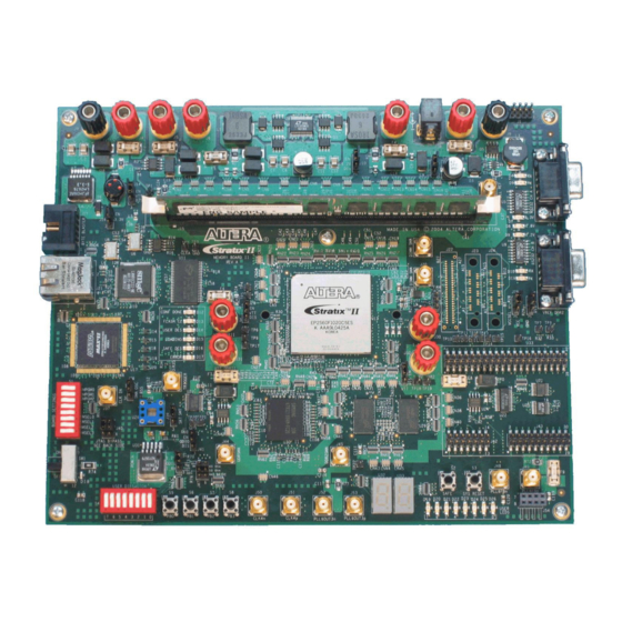
Stratix II Memory Board 2 Rev A User Guide Rev 0.1 Stratix II Memory Board 2 Layout Guidelines - This document provides PCB layout design guidelines for the board. 2 Getting Started This section describes how to get started with the board, including describing the board components, explaining how to set up the board, and describing how to perform the preloaded diagnostic tests. -
Page 7: Hardware Requirements
SDRAM module, Micron part number MT9HTF3272AG-53B or compatible part. 2.1.4 Software Requirements Refer to the Stratix II Memory Board 2 Data Sheet for information on the board components and their locations. You should install the following software before you begin using the board. -
Page 8: Restore Archived Projects
Stratix II Memory Board 2 Rev A User Guide Rev 0.1 • .sof files – Several .sof and .pof files are used to configure the Altera devices on the S2MB2 to run the tests. • The software on the S2MB2, Stratix II Edition CDROM. -
Page 9: Next Steps
This user guide contains the following chapters to help you get started working with the board: “Board Interfaces” in section 2.2 explains how to setup and configure the Stratix II Memory Board 2. “Run the Preloaded Diagnostic Tests” in section 2.3 describes how to set up and run each preloaded design and the required equipment. -
Page 10: Run The Preloaded Diagnostic Tests
A subset of the diagnostic tests are loaded into the Stratix II Memory Board 2’s Flash memory. If the S2MB2 does have preloaded diagnostic tests already in Flash, then at power up the MAX®... -
Page 11: User I/O Test
Stratix II Memory Board 2 Rev A User Guide Rev 0.1 Diagnostic Test PageName MPGM(2) MPGM(1) MPGM(0) User I/O and Nios Stamp Safe (Note 1) DDR2 SDRAM DIMM Zero Closed Closed Closed DDR2 SDRAM Devices Closed Closed Open QDRII SRAM Device(s) -
Page 12: Nios Stamp Features Test
Stratix II Memory Board 2 Rev A User Guide Rev 0.1 Figure 5 through Figure 7, show the applicable GUI pages. 1. Choose Open Port > RS232 Com1 (BTS menu) to open the COM1 port. 2. Click the UserIO tab. - Page 13 Stratix II Memory Board 2 Rev A User Guide Rev 0.1 10/100-Mbit Ethernet cable 2.3.2.2 Test Setup Perform the following steps to set up the Nios Stamp test. 1. Move the power switch to the OFF position. 2. Connect one end of the RS-232 cable to port A (J12) of the board, and the other end of the cable to the COM1 port of the computer.
-
Page 14: Ddr2 Sdram Dimm Test
9. Verify that the LEDs on the Ethernet connector blink several times. 10. If the Stratix II high-speed development board is not connected to a live network, the Ethernet tests cannot work correctly. In this case, look for the following message in the BTS message window in the bottom of the GUI. -
Page 15: Ddr2 Sdram Devices Test
4. Move the power switch to the ON position. 5. Press the SYS_RESETn (S3) pushbutton to reload the FPGA. 6. Confirm that the Stratix II device has finished configuration (the CONF_DONEn LED (D12) illuminates). The Error LED (D17) will illuminate if there is an error. -
Page 16: Qdrii Sram Device(S) Test
3. Move the power switch to the ON position. 4. Press the SYS_RESETn (S3) pushbutton to reload the FPGA. 5. Confirm that the Stratix II device has finished configuration (the CONF_DONEn LED (D12) illuminates). The Error LED (D17) will illuminate if there is an error. -
Page 17: Diagnostic Tests
The diagnostic tests that follow are for execution of the individual batch files using the pc to load the files through the JTAG port onto the Stratix II. The User IO and NIOS stamp functions are exercised using a prototype of the Board Test System (BTS). -
Page 18: Set Up The Board
Stratix II Memory Board 2 Rev A User Guide Rev 0.1 3.1.1 Set up the Board S2MB2 requires a number of jumpers, switch settings, and other hardware setup before testing should begin. See Figure 3 for the location of the switches and jumpers. - Page 19 Stratix II Memory Board 2 Rev A User Guide Rev 0.1 J10, J11 J16, J14 J26, J27 J40, J36 J39, J41 J46, J47 Figure 3. S2MB2 Board • NIOS Proto1 test card w/ modified resister value – A NIOS Proto1 test card is used to help verify the Proto 1 interface.
-
Page 20: Power Up Procedure
Stratix II Memory Board 2 Rev A User Guide Rev 0.1 Power JTAG RS-232 Ethernet Proto1 Card Figure 4. S2MB2 with Cables 3.1.2 Power up Procedure Insert the power connector into the socket. A red LED (D8) on the Proto1 test card should come on. -
Page 21: Nios Stamp Features Test
Stratix II Memory Board 2 Rev A User Guide Rev 0.1 • Run the batch file by double clicking on the file name: “bts_test.bat” (if using a USB blaster). This starts downloading the NIOS programming, where a DOS command window opens and the scripts start executing. Once the programming is finished it loads the user interface GUI. - Page 22 Stratix II Memory Board 2 Rev A User Guide Rev 0.1 There were 0 error(s). Test Complete • Warning: Running the Flash tests will corrupt the designs in flash memory. You will have to reprogram the flash to the factory image after running these tests.
-
Page 23: Ddr2 Sdram Dimm
LED5 are simply to indicate the design is running. 3.1.9 Downloading Factory Image This downloads the default Stratix II images to the on board flash for the Max/Max II and Flash FPP configuration method. To download the images to the flash, double click on the “Program_Flash.bat” file. -
Page 24: Troubleshooting
Stratix II Memory Board 2 Rev A User Guide Rev 0.1 Please check that the USB-Blaster is connected to the Board. Press any key to continue . . . Aug 2, 2004 5:35:26 PM - (INFO) nios2-flash-programmer: Launching Quartus Progra mmer to download: ..\sofs\stratix2_hsio_flash_download.sof... -
Page 25: Diagnostic Test Details
(BTS), and the tool command language (TCL)-based application using the Quartus® II TCL application program interface (API). The BTS host application uses an RS-232 cable connected to the Stratix II Memory Board 2 to communicate with the Nios system. - Page 26 The Nios system can then interface to each of the peripherals being tested. The Nios II target interprets and executes pre-defined commands and tests issued by the BTS host application. These commands test the Stratix II Memory Board 2 development board’s User I/O and Nios features.
- Page 27 Stratix II Memory Board 2 Rev A User Guide Rev 0.1 The host application only monitors the dipswitch and pushbuttons once the Enable Polling button is pushed. The GUI’s dipswitch and pushbuttons then display the boards User I/O features. The board’s seven-segment display and LEDs reflect the value selected on the slider, and the checkbox values.
-
Page 28: Ddr2 Sdram Dimm Test
Stratix II Memory Board 2 Rev A User Guide Rev 0.1 Figure 7 BTS GUI NIOS Stamp Tab The two memory interfaces perform walking ones tests on the address and data of each interface. Messages regarding the tests are reported in the NIOS Stamp Msgs window. -
Page 29: Ddr2 Sdram Devices Test
Stratix II Memory Board 2 Rev A User Guide Rev 0.1 The DDR2 SDRAM DIMM test uses a hardware state machine included in the DDR2 MegaCore® function, and a DDR2 SDRAM DIMM to test the DDR2 SDRAM interface. The example driver is a self-test module that issues read and write commands to the controller, and checks the read data to produce the pass/fail and test complete signals. - Page 30 Stratix II Memory Board 2 Rev A User Guide Rev 0.1 This section describes the QDRII SRAM Devices test. Refer to “QDRII SRAM Device(s)” in section 3.1.8 for information on how to perform the test. The QDRII SRAM test uses the Altera® QDRII SRAM MegaCore® function, the example driver provided with the MegaCore function, and some logic to indicate the status of the test.
-
Page 31: Max/Max Ii Configuration Controller
Figure 8 shows the block diagram of the MAX/MAX II configuration circuitry of the Stratix II Memory Board 2. The design uses 129 of 256 macrocells in the EPM1270F256 device. There are 104 of 120 I/Os used in the design. The... - Page 32 Stratix II devices to allow the MAX/MAX II device to control the configuration inputs and monitor the Stratix II configuration status outputs. The below memory map is used for Stratix II Memory Board 2. The large 16MB Flash has more then enough room to store items useful for demos such as image files and small video files in the “PLD Design X / Other”...
- Page 33 • SAFE design will be loaded if the User Design fails to load. • USER LEDs are driven through the MAX/MAX II from the Stratix II • LOADING LED blinks during a configuration attempt • CONF_DONEn LED lights when the Factory Default image was loaded •...
Need help?
Do you have a question about the Stratix II and is the answer not in the manual?
Questions and answers