Altera Stratix IV GX Reference Manual
Fpga development board, 530 edition
Hide thumbs
Also See for Stratix IV GX:
- User manual (30 pages) ,
- Reference manual (44 pages) ,
- Manual (30 pages)
Table of Contents
Advertisement
Quick Links
Download this manual
See also:
User Manual
Advertisement
Table of Contents

Related Manuals for Altera Stratix IV GX


Summary of Contents for Altera Stratix IV GX
- Page 1 Stratix IV GX FPGA Development Board, 530 Edition Reference Manual Stratix IV GX FPGA Development Board, 530 Edition Reference Manual 101 Innovation Drive San Jose, CA 95134 www.altera.com MNL-01060-1.0 Subscribe...
- Page 2 © 2010 Altera Corporation. All rights reserved. ALTERA, ARRIA, CYCLONE, HARDCOPY, MAX, MEGACORE, NIOS, QUARTUS and STRATIX are Reg. U.S. Pat. & Tm. Off. and/or trademarks of Altera Corporation in the U.S. and other countries. All other trademarks and service marks are the property of their respective holders as described at www.altera.com/common/legal.html.
-
Page 3: Table Of Contents
Featured Device: Stratix IV GX Device ........ - Page 4 How to Contact Altera ........
-
Page 5: Chapter 1. Overview
Design advancements and innovations, such as the 8.5 Gbps transceiver modules, the PCI Express hard IP implementation, and programmable power technology ensure that designs implemented in the Stratix IV GX FPGAs operate faster, with lower power than in previous FPGA families. - Page 6 Two-line character LCD display ■ One configuration done LED ■ One transmit/receive LED (TX/RX) per HSMC interface ■ Four PCI Express LEDs ■ Four Ethernet LEDs ■ Stratix IV GX FPGA Development Board, 530 Edition Reference Manual November 2010 Altera Corporation...
- Page 7 PCI Express edge connector power ■ On-Board power measurement circuitry ■ Mechanical ■ PCI Express half-length full-height (6.6” x 4.376”) ■ PCI Express chassis or bench-top operation ■ November 2010 Altera Corporation Stratix IV GX FPGA Development Board, 530 Edition Reference Manual...
-
Page 8: Development Board Block Diagram
Chapter 1: Overview Development Board Block Diagram Development Board Block Diagram Figure 1–1 shows the block diagram of the Stratix IV GX FPGA Development Board, 530 Edition. Figure 1–1. Stratix IV GX FPGA Development Board, 530 Edition Block Diagram Port A... -
Page 9: Introduction
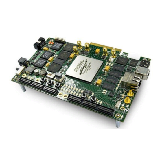
2. Board Components Introduction This chapter introduces all the important components on the Stratix IV GX FPGA Development Board, 530 Edition. Figure 2–1 illustrates major component locations Table 2–1 provides a brief description of all features of the board. A complete set of schematics, a physical layout database, and GERBER files for the development board reside in the Stratix IV GX development kit documents directory. -
Page 10: Board Overview
Fan Power Header Clock Output SMA Connector (J9) Table 2–1 describes the components and lists their corresponding board references. Table 2–1. Stratix IV GX FPGA Development Board, 530 Edition Components (Part 1 of 3) Board Reference Type Description Featured Devices FPGA EP4SGX530KH40, 1517-pin BGA. - Page 11 Chapter 2: Board Components 2–3 Board Overview Table 2–1. Stratix IV GX FPGA Development Board, 530 Edition Components (Part 2 of 3) Board Reference Type Description Load LED Illuminates during embedded USB-Blaster data transfers. Error LED Illuminates when the FPGA configuration from flash fails.
- Page 12 2–4 Chapter 2: Board Components Board Overview Table 2–1. Stratix IV GX FPGA Development Board, 530 Edition Components (Part 3 of 3) Board Reference Type Description Memory Devices U5, U12, U18, DDR3 x64 bottom port A single 64-bit 512 Mbyte memory port.
-
Page 13: Featured Device: Stratix Iv Gx Device
Featured Device: Stratix IV GX Device Featured Device: Stratix IV GX Device The Stratix IV GX FPGA Development Board, 530 Edition features the Stratix IV GX EP4SGX530KH40 device (U13) in a 1517-pin FineLine BGA package. For more information about the Stratix IV device family, refer to the Stratix IV Device Handbook. -
Page 14: I/O Resources
Name Channel Number of I/Os Table 2–4 lists the Stratix IV GX device pin count and usage by function on the development board. Table 2–4. Stratix IV GX Device Pin Count and Usage (Part 1 of 2) Function I/O Standard... -
Page 15: Migration Support
Chapter 2: Board Components 2–7 MAX II CPLD EPM2210 System Controller Table 2–4. Stratix IV GX Device Pin Count and Usage (Part 2 of 2) Function I/O Standard I/O Count Special Pins Clocks or Oscillators 2.5-V CMOS + LVDS 4 REFCLK Power or Temperature Sense 2.5-V CMOS10... - Page 16 FSM bus address FSM_A15 2.5-V AK32 FSM bus address FSM_A14 2.5-V AU33 FSM bus address FSM_A13 2.5-V AT33 FSM bus address FSM_A12 2.5-V AH30 FSM bus address FSM_A11 Stratix IV GX FPGA Development Board, 530 Edition Reference Manual November 2010 Altera Corporation...
- Page 17 FSM_D9 2.5-V FSM bus data FSM_D8 2.5-V FSM bus data FSM_D7 2.5-V FSM bus data FSM_D6 2.5-V FSM bus data FSM_D5 2.5-V FSM bus data FSM_D4 November 2010 Altera Corporation Stratix IV GX FPGA Development Board, 530 Edition Reference Manual...
- Page 18 SENSE_CS0n 2.5-V Power monitor 1 chip select SENSE_CS1n 2.5-V Power monitor frequency SENSE_ADN_F0 2.5-V Temperature monitor SMB clock SENSE_SMB_CLK 2.5-V AH32 Temperature monitor SMB data SENSE_SMB_DATA Stratix IV GX FPGA Development Board, 530 Edition Reference Manual November 2010 Altera Corporation...
- Page 19 155 MHz oscillator enable CLK155_EN 2.5-V — 156 MHz oscillator enable CLK156_EN 2.5-V AC34 50 MHz clock input CLKIN_50 2.5-V — 125 MHz configuration clock CLK_CONFIG November 2010 Altera Corporation Stratix IV GX FPGA Development Board, 530 Edition Reference Manual...
-
Page 20: Configuration, Status, And Setup Elements
The USB-Blaster is implemented using a type-B USB connector (J7), a FTDI USB 2.0 PHY device (U39), and an Altera MAX II CPLD (U30). This allows the configuration of the FPGA using a USB cable directly connected between the USB port on the board (J7) and a USB port of a PC running the Quartus II software. - Page 21 SW6.2 Installed HSMC HSMC Port B Card Analog Switch JTAG Master/Slave HSMB_JTAG_EN SW6.3 PCI Express PCI Express Edge Motherboard Connector Analog Switch JTAG Master/Slave PCIE_JTAG_EN SW6.4 November 2010 Altera Corporation Stratix IV GX FPGA Development Board, 530 Edition Reference Manual...
-
Page 22: Fpga Programming From Flash Memory
GUI interfaces. For this setting, push the left-most switch in the down position and all other switches in the up position. Flash Programming Flash programming is possible through a variety of methods using the Stratix IV GX device. The default method is to use the factory design called the Board Update Portal. This design is an embedded webserver, which serves the Board Update Portal web page. - Page 23 0x02000000 – 0x0349FFFF zipfs—HTML, Web Content 5,898 0x01A60000 – 0x01FFFFFF Factory Software 5,898 0x014C0000 – 0x01A5FFFF Factory Hardware 21,627 0x00020000 – 0x014BFFFF PFL Option Bits 0x00018000 – 0x0001FFFF November 2010 Altera Corporation Stratix IV GX FPGA Development Board, 530 Edition Reference Manual...
-
Page 24: Fpga Programming Over External Usb-Blaster
Green LED. Illuminates when the MAX II CPLD EPM2210 System Controller is Loading actively configuring the FPGA. Driven by the MAX II CPLD EPM2210 System Controller wire-OR'd with the Embedded Blaster CPLD. Stratix IV GX FPGA Development Board, 530 Edition Reference Manual November 2010 Altera Corporation... -
Page 25: Setup Elements
Board settings DIP switch ■ ■ JTAG control DIP switch ■ PCI Express control DIP switch ■ Reset configuration push-button switch Rotary switch ■ November 2010 Altera Corporation Stratix IV GX FPGA Development Board, 530 Edition Reference Manual... -
Page 26: Board Settings Dip Switch
DIP switch JTAG Control DIP Switch The JTAG control DIP switch is provided to either remove or include devices in the active JTAG chain. However, the Stratix IV GX FPGA device is always in the JTAG chain. Table 2–13 shows the switch controls and its descriptions. -
Page 27: Pci Express Control Dip Switch
Valid locations include 0 and 1 for the two pages in flash reserved for FPGA designs. November 2010 Altera Corporation Stratix IV GX FPGA Development Board, 530 Edition Reference Manual... -
Page 28: Rotary Switch
Bank 6 I/O power (HSMC port B) S4VCCIO_B6 VCCIO_B1 Bank 1 I/O power (FSM bus) S4VCCIO_B1B2 VCCIO_B2 Bank 2 I/O power (FSM bus) VCCIO_B3A Bank 3A I/O power (HDMI) S4VCCIO_B3A Stratix IV GX FPGA Development Board, 530 Edition Reference Manual November 2010 Altera Corporation... -
Page 29: Clock Circuitry
Manufacturer Board Reference Description Manufacturer Part Number Website 16-position rotary Grayhill Corporation 94HCB16WT www.grayhill.com switch Clock Circuitry This section describes the board's clock inputs and outputs. November 2010 Altera Corporation Stratix IV GX FPGA Development Board, 530 Edition Reference Manual... -
Page 30: Stratix Iv Gx Fpga Clock Inputs
Stratix IV GX FPGA Development Board, 530 Edition global clock inputs. The development board’s transceiver reference clock inputs are shown in Figure 2–7. Figure 2–6. Stratix IV GX FPGA Development Board, 530 Edition Global Clock Inputs To REFCLK Clock Inputs CLK7p CLK13p... - Page 31 Connector Table 2–20 shows the external clock inputs for the Stratix IV GX FPGA Development Board, 530 Edition. Table 2–20. Stratix IV GX FPGA Development Board, 530 Edition Clock Inputs (Part 1 of 2) Source Schematic Signal Name I/O Standard...
- Page 32 2–24 Chapter 2: Board Components Clock Circuitry Table 2–20. Stratix IV GX FPGA Development Board, 530 Edition Clock Inputs (Part 2 of 2) Source Schematic Signal Name I/O Standard Description 155.52 MHz oscillator which drives the transceiver reference clock input with 100 Ω...
-
Page 33: Stratix Iv Gx Fpga Clock Outputs
1.5V HSTL Class I, 50 Ω OCT Table 2–21 shows the clock outputs for the Stratix IV GX FPGA Development Board, 530 Edition. Table 2–21. Stratix IV GX FPGA Development Board, 530 Edition Clock Outputs (Part 1 of 2) Connector Schematic Signal Name I/O Standard Description 2.5-V... -
Page 34: General User Input/Output
2–26 Chapter 2: Board Components General User Input/Output Table 2–21. Stratix IV GX FPGA Development Board, 530 Edition Clock Outputs (Part 2 of 2) Connector Schematic Signal Name I/O Standard Description HSMB_CLK_OUT_P1 Samtec HSMC LVDS or 2.5-V LVDS output or two 2.5-V CMOS outputs. -
Page 35: User-Defined Dip Switches
Board reference S2 is the CPU reset push-button switch, CPU_RESETn, which is an input to both the Stratix IV GX device and MAX II CPLD EPM2210 System Controller. The CPU_RESETn is intended to be the master reset signal for the FPGA design loaded into the Stratix IV GX device. -
Page 36: User-Defined Leds
LEDs from the designs loaded into the Stratix IV GX device. The LEDs illuminate when a logic 0 is driven, and turns off when a logic 1 is driven. There is no board-specific function for these LEDs. -
Page 37: Hsmc User-Defined Leds
14-pin header, so it can be easily removed for access to components under the display. You can also use the header for debugging or other purposes. November 2010 Altera Corporation Stratix IV GX FPGA Development Board, 530 Edition Reference Manual... - Page 38 DB0–DB7 Data bus, software selectable 4-bit or 8-bit mode The particular model used does not have a backlight and the LCD drive pin is not connected. Stratix IV GX FPGA Development Board, 530 Edition Reference Manual November 2010 Altera Corporation...
-
Page 39: Components And Interfaces
The PCIE_REFCLK_P signal is a 100-MHz differential input that is driven from the PC motherboard on this board through the edge connector. This signal is connected directly to a Stratix IV GX REFCLK input pin pair using DC coupling. This clock is terminated on the motherboard and therefore, no on-board termination is required. - Page 40 The JTAG and SMB are optional signals in the PCI Express specification. Both types of signals are wired to the Stratix IV GX device but are not required for normal operation. The PCI Express control DIP switch allows the presence detect grounding to be altered to enable a ×1, ×4, or ×8 width edge connector.
-
Page 41: 10/100/1000 Ethernet
The device is an auto-negotiating Ethernet PHY with an SGMII interface to the FPGA. The Stratix IV GX device can communicate with the LVDS interfaces at up to 1.6 Gbps, which is faster than 1.25 Gbps for SGMII. The MAC function must be provided in the FPGA for typical networking applications. - Page 42 Table 2–36. Ethernet PHY Component Reference and Manufacturing Information Manufacturing Manufacturer Board Reference Description Manufacturer Part Number Website Marvel Ethernet PHY BASE-T device 88E1111-B2-CAAIC000 www.marvell.com Semiconductor Stratix IV GX FPGA Development Board, 530 Edition Reference Manual November 2010 Altera Corporation...
-
Page 43: High-Speed Mezzanine Cards
These HSMC interfaces support both single-ended and differential signaling. The HSMC interface also allows JTAG, SMB, clock outputs and inputs, as well as power for compatible HSMC cards. The HSMC is an Altera-developed open specification, which allows you to expand the functionality of the development board through the addition of daughtercards. - Page 44 Transceiver RX bit 1n HSMA_RX_N1 J1.29 Transceiver TX bit 0 HSMA_TX_P0 J1.30 Transceiver RX bit 0 HSMA_RX_P0 J1.31 Transceiver TX bit 0n HSMA_TX_N0 J1.32 Transceiver RX bit 0n HSMA_RX_N0 Stratix IV GX FPGA Development Board, 530 Edition Reference Manual November 2010 Altera Corporation...
- Page 45 LVDS RX bit 5n or CMOS bit 27 HSMA_RX_D_N5 J1.83 LVDS TX bit 6 or CMOS bit 28 AH10 HSMA_TX_D_P6 J1.84 LVDS RX bit 6 or CMOS bit 29 HSMA_RX_D_P6 November 2010 Altera Corporation Stratix IV GX FPGA Development Board, 530 Edition Reference Manual...
- Page 46 LVDS RX bit 14 or CMOS bit 65 HSMA_RX_D_P14 J1.139 LVDS TX bit 14n or CMOS bit 66 AB12 HSMA_TX_D_N14 J1.140 LVDS RX bit 14n or CMOS bit 67 HSMA_RX_D_N14 Stratix IV GX FPGA Development Board, 530 Edition Reference Manual November 2010 Altera Corporation...
- Page 47 Transceiver TX bit 5n HSMB_TX_N5 J2.12 Transceiver RX bit 5n HSMB_RX_N5 J2.13 Transceiver TX bit 4 HSMB_TX_P4 J2.14 Transceiver RX bit 4 HSMB_RX_P4 J2.15 Transceiver TX bit 4n HSMB_TX_N4 November 2010 Altera Corporation Stratix IV GX FPGA Development Board, 530 Edition Reference Manual...
- Page 48 LVDS TX bit 1n or CMOS bit 10 HSMB_TX_D_N1 J2.56 LVDS RX bit 1n or CMOS bit 11 HSMB_RX_D_N1 J2.59 LVDS TX bit 2 or CMOS bit 12 HSMB_TX_D_P2 Stratix IV GX FPGA Development Board, 530 Edition Reference Manual November 2010 Altera Corporation...
- Page 49 LVDS TX bit 10 or CMOS bit 48 HSMB_TX_D_P10 J2.114 LVDS RX bit 10 or CMOS bit 49 HSMB_RX_D_P10 J2.115 LVDS TX bit 10n or CMOS bit 50 HSMB_TX_D_N10 November 2010 Altera Corporation Stratix IV GX FPGA Development Board, 530 Edition Reference Manual...
- Page 50 User LED to show RX data activity on AT10 HSMB_RX_LED HSMC Port B 2.5-V User LED to show TX data activity on HSMC AH33 HSMB_TX_LED Port B Stratix IV GX FPGA Development Board, 530 Edition Reference Manual November 2010 Altera Corporation...
-
Page 51: Hdmi Video Output
HDMI Video Output The Stratix IV GX FPGA Development Board, 530 Edition supports a single HDMI video output port based on the Analog Devices AD9889B HDMI transmitter device. With the capability of up to 80 MHz operation, this device supports all video resolutions from 480i to 1080i and UXGA at 60 Hz. - Page 52 AK26 HDMI_D6 U25.A4 Video data bus AN26 HDMI_D7 U25.B5 Video data bus AP27 HDMI_D8 U25.A5 Video data bus AN27 HDMI_D9 U25.B6 Video data bus AV28 HDMI_D10 Stratix IV GX FPGA Development Board, 530 Edition Reference Manual November 2010 Altera Corporation...
- Page 53 Table 2–41. HDMI Video Output Connector Component Reference and Manufacturing Information Manufacturing Manufacturer Board Reference Description Manufacturer Part Number Website HDMI transmitter Analog Devices AD9889BBBCZ-80 www.analog.com November 2010 Altera Corporation Stratix IV GX FPGA Development Board, 530 Edition Reference Manual...
-
Page 54: Sdi Video Input/Output
SMPTE 259M Slower Table 2–43 summarizes the SDI video output interface pin assignments. The signal names and directions are relative to the Stratix IV GX FPGA. Table 2–43. SDI Video Output Interface Pin Assignments, Schematic Signal Names, and Functions Board Schematic... - Page 55 Table 2–45 summarizes the SDI video input interface pin assignments. The signal names and directions are relative to the Stratix IV GX FPGA. Table 2–45. SDI Video Input Interface Pin Assignments, Schematic Signal Names, and Functions MAX II CPLD EPM2210...
-
Page 56: Memory
Chapter 2: Board Components Memory Memory This section describes the board’s memory interface support, signal names, types, and connectivity relative to the Stratix IV GX device. The board has the following memory interfaces: ■ DDR3 Bottom Port DDR3 Top Port ■... - Page 57 DDR3BOT_DQS_P1 U5.B7 Data strobe N byte lane 1 AW13 DDR3BOT_DQS_N1 U12.E3 Data bus byte lane 2 AT16 DDR3BOT_DQ16 U12.F7 Data bus byte lane 2 AW16 DDR3BOT_DQ17 November 2010 Altera Corporation Stratix IV GX FPGA Development Board, 530 Edition Reference Manual...
- Page 58 AN19 DDR3BOT_DQ43 U18.A7 Data bus byte lane 5 AT18 DDR3BOT_DQ44 U18.A2 Data bus byte lane 5 AU18 DDR3BOT_DQ45 U18.B8 Data bus byte lane 5 AW18 DDR3BOT_DQ46 Stratix IV GX FPGA Development Board, 530 Edition Reference Manual November 2010 Altera Corporation...
- Page 59 Table 2–47. DDR3 Component Reference and Manufacturing Information Manufacturing Manufacturer Board Reference Description Manufacturer Part Number Website U5, U12, U18, U24 8 M × 16-bit × 8 banks, 667M, CL9 Micron MT41J64M16LA-15E www.micron.com November 2010 Altera Corporation Stratix IV GX FPGA Development Board, 530 Edition Reference Manual...
-
Page 60: Ddr3 Top Port
Column address select DDR3TOP_CASn U14.L2 Chip select DDR3TOP_CSn U14.L3 Write enable DDR3TOP_WEn U14.K1 Termination enable DDR3TOP_ODT U14.K9 Clock enable DDR3TOP_CKE U14.J7 Clock P DDR3TOP_CK_P U14.K7 Clock N DDR3TOP_CK_N Stratix IV GX FPGA Development Board, 530 Edition Reference Manual November 2010 Altera Corporation... -
Page 61: Qdrii+ Top Port 0
14.4 Gbps for writing. The internal bus in the FPGA is typically 2 or 4 times the width at full rate or half rate respectively. For example, a 400 MHz 18-bit interface becomes a 200 MHz 72 bit bus. November 2010 Altera Corporation Stratix IV GX FPGA Development Board, 530 Edition Reference Manual... - Page 62 Table 2–50 lists the QDRII+ top port 0 pin assignments, signal names, and functions. The signal names and types are relative to the Stratix IV GX device in terms of I/O setting and direction. Table 2–50. QDRII+ Top Port 0 Pin Assignments, Signal Names and Functions (Part 1 of 2)
- Page 63 Read data bus QDR2TOP0_Q0 U22.A11 Read clock P QDR2TOP0_CQ_P U22.A1 Read clock N QDR2TOP0_CQ_N U22.A8 Read port select QDR2TOP0_RPSn U22.P6 Read data valid QDR2TOP0_QVLD U22.H1 DLL enable QDR2TOP0_DOFFn November 2010 Altera Corporation Stratix IV GX FPGA Development Board, 530 Edition Reference Manual...
-
Page 64: Qdrii+ Top Port 1
Table 2–52 lists the QDRII+ top port 1 pin assignments, signal names, and functions. The signal names and types are relative to the Stratix IV GX device in terms of I/O setting and direction. Table 2–52. QDRII+ Top Port 1 Pin Assignments, Schematic Signal Names, and Functions (Part 1 of 3) - Page 65 QDR2TOP1_Q11 U7.D3 Read data bus QDR2TOP1_Q10 U7.B2 Read data bus QDR2TOP1_Q9 U7.B11 Read data bus QDR2TOP1_Q8 U7.C10 Read data bus QDR2TOP1_Q7 U7.E11 Read data bus QDR2TOP1_Q6 November 2010 Altera Corporation Stratix IV GX FPGA Development Board, 530 Edition Reference Manual...
-
Page 66: Ssram
The read latency for any address is two clocks, in which at 250 MHz, the latency is 10 ns and at 50 MHz, the latency is 40 ns. The write latency is one clock. Stratix IV GX FPGA Development Board, 530 Edition Reference Manual November 2010 Altera Corporation... - Page 67 Table 2–54 lists the SSRAM pin assignments, signal names, and functions. The signal names and types are relative to the Stratix IV GX device in terms of I/O setting and direction. Table 2–54. SSRAM Pin Assignments, Schematic Signal Names, and Functions (Part 1 of 3)
- Page 68 Byte write enable AK30 SRAM_BWEn U30.B7 Global write enable AC29 SRAM_GWn U30.A8 Address status controller AM31 SRAM_ADSCn U30.B9 Address status processor AG28 SRAM_ADSPn U30.A9 Address valid AU32 SRAM_ADVn Stratix IV GX FPGA Development Board, 530 Edition Reference Manual November 2010 Altera Corporation...
-
Page 69: Flash
Table 2–56 lists the flash pin assignments, signal names, and functions. The signal names and types are relative to the Stratix IV GX device in terms of I/O setting and direction. Table 2–56. Flash Pin Assignments, Schematic Signal Names, and Functions (Part 1 of 3) - Page 70 U32.F2 Data bus FSM_D1 U32.E6 Data bus FSM_D0 U32.D4 Clock AF26 FLASH_CLK U32.B4 Reset AL30 FLASH_RESETn U32.F8 Chip enable AU31 FLASH_CEn U32.G8 Output enable AG27 FLASH_OEn Stratix IV GX FPGA Development Board, 530 Edition Reference Manual November 2010 Altera Corporation...
-
Page 71: Power Supply
An on-board multi-channel analog-to-digital converter (ADC) is used to measure both the voltage and current for several specific board rails. The power utilization is displayed in a GUI that graphs power consumption versus time. November 2010 Altera Corporation Stratix IV GX FPGA Development Board, 530 Edition Reference Manual... -
Page 72: Power Distribution System
(4.77 A with full HSMCs) 0.69 A 0.051 A S4 VCCA_PLL BEAD 3.3V 3.3 V HSMC Port A and B, SDI 4.050 A ICS 8543 LVDS Clock Buffer Stratix IV GX FPGA Development Board, 530 Edition Reference Manual November 2010 Altera Corporation... -
Page 73: Power Measurement
ADC to measure voltage and current. A serial peripheral interface (SPI) bus connects these ADC devices to the MAX II CPLD EPM2210 System Controller as well as the Stratix IV GX FPGA. -
Page 74: Temperature Sense
Temperature Sense Temperature monitoring for the Stratix IV GX FPGA die is achieved with a MAX1619 temperature sense device. The MAX1619 device connects to the MAX II CPLD EPM2210 System Controller and the Stratix IV GX device by a 2-wire SMB interface. -
Page 75: Statement Of China-Rohs Compliance
(2) X* indicates that the concentration of the hazardous substance of at least one of all homogeneous materials in the parts is above the relevant threshold of the SJ/T11363-2006 standard, but it is exempted by EU RoHS. November 2010 Altera Corporation Stratix IV GX FPGA Development Board, 530 Edition Reference Manual... - Page 76 2–68 Chapter 2: Board Components Statement of China-RoHS Compliance Stratix IV GX FPGA Development Board, 530 Edition Reference Manual November 2010 Altera Corporation...
-
Page 77: Additional Information
(Software Licensing) Email authorization@altera.com Note to Table: (1) You can also contact your local Altera sales office or sales representative. Typographic Conventions The following table shows the typographic conventions this document uses. Visual Cue Meaning Indicate command names, dialog box titles, dialog box options, and other GUI Bold Type with Initial Capital labels. - Page 78 The envelope links to the Email Subscription Management Center page of the Altera website, where you can sign up to receive update notifications for Altera documents. Stratix IV GX FPGA Development Board, 530 Edition Reference Manual November 2010 Altera Corporation...
Need help?
Do you have a question about the Stratix IV GX and is the answer not in the manual?
Questions and answers