
Related Manuals for Altera Stratix II GX PCI Express


Summary of Contents for Altera Stratix II GX PCI Express
- Page 1 Stratix II GX PCI Express Development Board Reference Manual 101 Innovation Drive San Jose, CA 95134 Document Version: 1.0.1 (408) 544-7000 www.altera.com Document Date: April 2007...
- Page 2 Altera Corporation in the U.S. and other countries. All other product or service names are the property of their respective holders. Al- tera products are protected under numerous U.S.
-
Page 3: Table Of Contents
Contents About this Manual Revision History ............................v How to Contact Altera ..........................v Typographic Conventions........................vi Chapter 1. Introduction General Description..........................1-1 Board Features ........................... 1-1 Block Diagram ........................... 1-2 Handling the Board ..........................1-3 Chapter 2. Board Components & Interfaces Board Overview............................ - Page 4 Power Supply ............................2-55 Power Supply for Each Component ..................... 2-55 Components Attached to Each Power Rail ................. 2-56 Power Distribution System ......................2-58 Termination ............................2-60 DDR2 Memory ..........................2-60 QDRII Memory ..........................2-60 PCI Express ............................2-60 Altera Corporation Preliminary...
-
Page 5: About This Manual
® ® Altera Stratix II GX family of devices and the Stratix II GX PCI Express development board. How to Contact For the most up-to-date information about Altera products, go to the Altera world-wide web site at www.altera.com. For technical support on Altera this product, go to www.altera.com/mysupport. -
Page 6: Typographic Conventions
The warning indicates information that should be read prior to starting or continuing the procedure or processes The angled arrow indicates you should press the Enter key. The feet direct you to more information on a particular topic. Altera Corporation Preliminary August 2006... -
Page 7: Chapter 1. Introduction
Because the Stratix II GX embedded transceivers can implement the entire PCIe interface on one device, the Stratix II GX PCI Express development board offers a high-bandwidth, low-latency, power- efficient PCIe solution with sufficient LEs for your applications. -
Page 8: Block Diagram
SMA connector for external clock input and output ● Block Diagram Figure 1–1 shows a functional block diagram of the Stratix II GX PCI Express development board. 1–2 Reference Manual Altera Corporation Stratix II GX PCI Express Development Board August 2006... -
Page 9: Handling The Board
Introduction Figure 1–1. Stratix II GX PCI Express Development Board HMC Port A HMC Port B MAX II Device 72 MB QDRII 1.8 V CMOS 1.8V HSTL 512 MB Flash (x36) 88E1111 1.8 V SSTL 1.8V HSTL 256 MB DDR2... - Page 10 Handling the Board 1–4 Reference Manual Altera Corporation Stratix II GX PCI Express Development Board August 2006...
-
Page 11: Chapter 2. Board Components & Interfaces
Stratix II GX PCI Express (PCIe) development board are included in the PCI Express Development Kit, Stratix II GX Edition in the following directory: <install path>/BoardDesignFiles Altera Corporation Reference Manual 2–1 August 2006 Stratix II GX PCI Express Development Board... - Page 12 155.25-MHz PCI Express x8 Flash Device (U3) Crystal (X4) Edge Connector Stratix II GX Device (U10) DDR2 32 x 16 Mbytes SDRAM (U5, U8, U11, U13) 2–2 Reference Manual Altera Corporation Stratix II GX PCI Express Development Board August 2006...
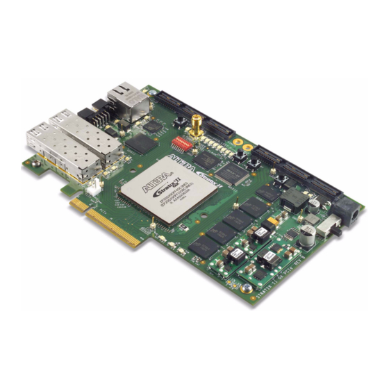
- Page 13 Figure 2–2 shows a diagonal view of the Stratix II GX PCIe development board. Figure 2–2. Diagonal View of the Stratix II GX PCIe Development Board Altera Corporation Reference Manual 2–3 August 2006 Stratix II GX PCI Express Development Board...
- Page 14 Small form pluggable cage allows for the connection of SFP 2–33 modules. SFP B Small form pluggable cage allows for the connection of SFP 2–33 modules. 2–4 Reference Manual Altera Corporation Stratix II GX PCI Express Development Board August 2006...
-
Page 15: Featured Device
Provides up to 63 DSP blocks for efficient implementation of high-performance filters SRAM process and other DSP functions ● Supports a wide range of external memory interfaces Altera Corporation Reference Manual 2–5 August 2006 Stratix II GX PCI Express Development Board... -
Page 16: Device Support
EP2SGX90FF1508 (default) and the EP2SGX130GF1508 devices. Figure 2–3 illustrates the available I/O bank resources on both the EP2SGX90FF1508 and the EP2SGX130GF1508 devices. (The numbers in parentheses represent the EP2SGX130GF1508 device resources.) 2–6 Reference Manual Altera Corporation Stratix II GX PCI Express Development Board August 2006... - Page 17 95 I/O 100 I/O (104) (106) Note: Figure is package-top referenced. Figure 2–4 illustrates the available I/O mapping on both the EP2SGX90FF1508 and the EP2SGX130GF1508 devices. Altera Corporation Reference Manual 2–7 August 2006 Stratix II GX PCI Express Development Board...
- Page 18 ® the Quartus II Development Software Handbook and the Stratix II GX Device Handbook. 2–8 Reference Manual Altera Corporation Stratix II GX PCI Express Development Board August 2006...
- Page 19 FPLL7_CLK (hsma_clk1) REFCLK1 (xaui_refclk) REFCLK0 REFCLK1 (hsmca_clk2) CLK0 CLK1 (hsmca_clk0) (pcie_refclk) REFCLK0 (hsmb_clk1) CLK2 REFCLK1 (100m_refclk) (hsmb_clk0) CLK3 REFCLK0 REFCLK1 REFCLK0 FPLL8_CLK REFCLK1 (hsmcb_clk2) PLL6 PLL12 Altera Corporation Reference Manual 2–9 August 2006 Stratix II GX PCI Express Development Board...
- Page 20 2 In REFCLK inputs LVDS — 3 In Note to Table 2–3: High-speed mezzanine card, port B: Four XCVR channels are only available with EP2SGX130GF1508 devices. 2–10 Reference Manual Altera Corporation Stratix II GX PCI Express Development Board August 2006...
-
Page 21: Clocking Circuitry
Signal Propagates To From 100 MHz U21 (ICS8543 clock buffer), Pins 4 and 5 100M_OSC_P 100M_OSC_N User input SMA clock input 25 MHz Ethernet PHY ENET_25M_CLK Altera Corporation Reference Manual 2–11 August 2006 Stratix II GX PCI Express Development Board... -
Page 22: Configuration Schemes And Status Leds
“Configuration DIP Switch (S6)” on page 2–23) to remove the HSMC A and B expansion connectors from the JTAG chain. Figure 2–7 shows the JTAG chain connections. 2–12 Reference Manual Altera Corporation Stratix II GX PCI Express Development Board August 2006... - Page 23 For more information about: ■ JTAG configuration, refer to Appendix A of the PCI Express Development Kit, Stratix II GX Edition Getting Started User Guide. ■ Programming Altera devices, refer to the Configuration Handbook. Altera Corporation Reference Manual 2–13 August 2006...
-
Page 24: Fpp Configuration
FLASH_A[24:0] DIP Switch FLASH_D[15:0] RUnLU FLASH_CEn CONFIG_MODE[1:0] FLASH_OEn FLASH_WEn DIPSW+PGM[2:0] MSEL[3:0] 10 kohm CFI FLASH 1.8V FLASH_A[25:0] 10 kohm FLASH_D[15:0] FLASH_CEn FLASH_OEn FLASH_WEn FPGA_RSTn FPGA_BYTEn FPGA_RYBYn 2–14 Reference Manual Altera Corporation Stratix II GX PCI Express Development Board August 2006... - Page 25 RUnLU pin control as well as some JTAG chain options. Refer to the “General User Interfaces” on page 2–21 for more information on the DIP switch. Altera Corporation Reference Manual 2–15 August 2006 Stratix II GX PCI Express Development Board...
-
Page 26: Flash Memory Configuration File Storage
0x0200.0000 FPGA Design 7 0x01FF.FFFF 0x01C0.0000 FPGA Design 6 0x01BF.FFFF 0x0180.0000 FPGA Design 5 0x017F.FFFF 0x0140.0000 FPGA Design 4 0x013F.FFFF 0x0100.0000 FPGA Design 3 0x00FF.FFFF 0x00C0.0000 2–16 Reference Manual Altera Corporation Stratix II GX PCI Express Development Board August 2006... -
Page 27: Max Ii Cpld Configuration Controller
80 ms of the end of a fundamental reset (release of the PERSTn pin). This can be a power-on-reset where the PWR GOOD signal is Altera Corporation Reference Manual 2–17 August 2006 Stratix II GX PCI Express Development Board... - Page 28 Description Signal Type Configuration clock 1.8-V CMOS out FPGA_CONFIG_DCLK FPGA_CONFIG_D(7:0) Configuration data bus 1.8-V CMOS out (8 bits) FPGA CONF_DONE pin 1.8-V CMOS in CONF_DONE connection 2–18 Reference Manual Altera Corporation Stratix II GX PCI Express Development Board August 2006...
- Page 29 For more information about the advanced parallel flash loader settings, refer to Chapter 2 of the Configuration Handbook, Configuring Stratix II and Stratix II GX Devices. Altera Corporation Reference Manual 2–19 August 2006 Stratix II GX PCI Express Development Board...
-
Page 30: Status And Channel Activity Leds
HSMC B RX Ethernet RX Ethernet TX SFP A RX SFP A TX SFP B RX SFP B TX PCI Express x1 PCI Express x2 PCI Express x3 2–20 Reference Manual Altera Corporation Stratix II GX PCI Express Development Board August 2006... -
Page 31: General User Interfaces
DEV_CLRn pin; when enabled in the Quartus II software, it will reset all Stratix II GX device registers. Pin AM22 can also be used as a standard input. Altera Corporation Reference Manual 2–21 August 2006 Stratix II GX PCI Express Development Board... -
Page 32: User-Defined Dip Switch (S5)
Schematic Signal Name Stratix II GX Device Pin USER_DIPSW0 USER_DIPSW1 USER_DIPSW2 USER_DIPSW3 USER_DIPSW4 USER_DIPSW5 USER_DIPSW6 USER_DIPSW7 Figure 2–9 shows the user-defined DIP switch board image. Figure 2–9. User-Defined DIP Switch Board Image 2–22 Reference Manual Altera Corporation Stratix II GX PCI Express Development Board August 2006... -
Page 33: User Leds (D9 Through D16)
In the open position, the selected signal is driven to logic 0. In the closed position, the selected signal is driven to a logic 1. Altera Corporation Reference Manual 2–23 August 2006 Stratix II GX PCI Express Development Board... -
Page 34: Board-Specific Leds
PCIe edge connector (L0x1, L0x4, L0x8) Yellow SFP A interface (TX & RX) Yellow SFP B interface (TX & RX) Yellow Gigabit Ethernet (TX & RX) Yellow 2–24 Reference Manual Altera Corporation Stratix II GX PCI Express Development Board August 2006... -
Page 35: Standard Communication Ports
The board features a x8 PCIe edge connector. The high speed PCIe signals are directly routed to two Stratix II GX device transceivers quads. The PCIe signals have 100 differential traces terminated on the receive-side Altera Corporation Reference Manual 2–25 August 2006 Stratix II GX PCI Express Development Board... - Page 36 AK18 pcie_smbdat AH20 pcie_tx_n[0] pcie_tx_n[1] pcie_tx_n[2] pcie_tx_n[3] pcie_tx_n[4] pcie_tx_n[5] pcie_tx_n[6] 2–26 Reference Manual Altera Corporation Stratix II GX PCI Express Development Board August 2006...
- Page 37 Voh/Vol levels that should be expected as inputs to the card. The clocks are terminated on the host and should DC couple to the Stratix II GX FPGA. Altera Corporation Reference Manual 2–27 August 2006 Stratix II GX PCI Express Development Board...
-
Page 38: Gigabit Ethernet (Gige) Interface (Rj1)
(GMII) or medium independent interface (MII). Figure 2–11 shows the interface between the Stratix II GX device’s MAC and the GigE PHY layer. 2–28 Reference Manual Altera Corporation Stratix II GX PCI Express Development Board August 2006... - Page 39 Board Reference Device Description RJ-45 single-port jack Table 2–21 lists manufacturing information. Table 2–21. Manufacturing Information Manufacturer Part Manufacturer Manufacturer Website Number HALO Electronics HFJ11-1G02E www.haloelectronics.com Altera Corporation Reference Manual 2–29 August 2006 Stratix II GX PCI Express Development Board...
- Page 40 Stratix II GX Device Pin Number enet_col enet_crs enet_gtx_clk enet_intn enet_mdc enet_mdio enet_resetn enet_rx_clk enet_rx_dv enet_rx_er enet_rxd[0] enet_rxd[1] enet_rxd[2] enet_rxd[3] enet_rxd[4] enet_rxd[5] enet_rxd[6] enet_rxd[7] enet_tx_clk enet_tx_en enet_tx_er enet_txd[0] enet_txd[1] enet_txd[2] 2–30 Reference Manual Altera Corporation Stratix II GX PCI Express Development Board August 2006...
- Page 41 DDR flip flops. The Stratix II GX PCIe development board can use either the GMII or RGMII interface. However, because of it’s simpler timing model, the GMII interface is preferred. Altera Corporation Reference Manual 2–31 August 2006 Stratix II GX PCI Express Development Board...
- Page 42 An IP core is also available from the Altera Megafunctions Partner Program (AMPP ) partner MorethanIP. The MorethanIP core has been used and tested on an existing Altera daughter card using the Nios II processor core and the MorethanIP TCP/IP driver software for the Nios II processor.
-
Page 43: Sfp A And B Interfaces (J6 And J7)
2–35. Figure 2–13 shows an SFP pin-out diagram. Figure 2–13. SFP Pin-Out Diagram SFP Module TXFault TXDisable Towards Bezel Towards FPGA MOD-DEF(2) MOD-DEF(1) MOD-DEF(0) Rate Select Altera Corporation Reference Manual 2–33 August 2006 Stratix II GX PCI Express Development Board... - Page 44 2–34 Reference Manual Altera Corporation Stratix II GX PCI Express Development Board August 2006...
-
Page 45: High-Speed Mezzanine Connectors A And B Interface
(plus dedicated clock input and output), a JTAG bus, 3.3 V, 12 volts, and GND. For more information about the Altera HSMC connectors, refer to the HSMC specifications on the Altera website, www.altera.com. The Stratix II GX device has 16 transceivers: Two are used by the SFP connectors and eight are used by the PCIe edge connector, which leaves only six for the HSMC connectors. - Page 46 2–36 Reference Manual Altera Corporation Stratix II GX PCI Express Development Board August 2006...
- Page 47 Altera Corporation Reference Manual 2–37 August 2006 Stratix II GX PCI Express Development Board...
- Page 48 2–38 Reference Manual Altera Corporation Stratix II GX PCI Express Development Board August 2006...
- Page 49 AP22 hsmb_led_rx AF25 hsmb_led_tx AV33 hsmb_rx_d_n[0] _AE36 hsmb_rx_d_n[1] AE38 hsmb_rx_d_n[10] AG35 hsmb_rx_d_n[11] AH36 hsmb_rx_d_n[12] AJ36 hsmb_rx_d_n[13] AK35 hsmb_rx_d_n[14] AL38 hsmb_rx_d_n[15] AP38 hsmb_rx_d_n[16] AT39 hsmb_rx_d_n[2] AG39 Altera Corporation Reference Manual 2–39 August 2006 Stratix II GX PCI Express Development Board...
- Page 50 AF39 hsmb_rx_d_p[3] AG38 hsmb_rx_d_p[4] AH39 hsmb_rx_d_p[5] AJ39 hsmb_rx_d_p[6] AK38 hsmb_rx_d_p[7] AN39 hsmb_rx_d_p[8] AE35 hsmb_rx_d_p[9] AF37 hsmb_rx_n[0] hsmb_rx_n[1] hsmb_rx_n[2] hsmb_rx_n[3] hsmb_rx_p[0] hsmb_rx_p[1] hsmb_rx_p[2] hsmb_rx_p[3] hsmb_scl AG30 2–40 Reference Manual Altera Corporation Stratix II GX PCI Express Development Board August 2006...
- Page 51 AB32 hsmb_tx_d_p[11] AC34 hsmb_tx_d_p[12] AD32 hsmb_tx_d_p[13] AC30 hsmb_tx_d_p[14] AB26 hsmb_tx_d_p[15] AD27 hsmb_tx_d_p[16] hsmb_tx_d_p[2] AA27 hsmb_tx_d_p[3] AD33 hsmb_tx_d_p[4] AB30 hsmb_tx_d_p[5] AB25 hsmb_tx_d_p[6] AD26 hsmb_tx_d_p[7] AE27 Altera Corporation Reference Manual 2–41 August 2006 Stratix II GX PCI Express Development Board...
- Page 52 The top-left is a x8 PCIe female adapter (right-angle) and the top-right is an ATCA mezzanine card (AMC) adapter. The lower two figures are Altera daughter card (PROTO1) adapters, which are typically 3” wide and can be any length upward.
-
Page 53: Jtag Interface
SLDHUB primitive) and the default USB-Blaster driver that Quartus II software installs for JTAG programming and SignalTap debugging. For more information on the JTAG chain, refer to “JTAG Configuration” on page 2–12. Altera Corporation Reference Manual 2–43 August 2006 Stratix II GX PCI Express Development Board... -
Page 54: Off-Chip Memory
Table 2–30. DDR2 SRAM Pin-Out (Part 1 of 5) Schematic Signal Name Stratix II GX Device Pin Number ddr2_a[0] AP16 ddr2_a[1] AH28 ddr2_a[10] AT30 ddr2_a[11] AN21 ddr2_a[12] AP28 2–44 Reference Manual Altera Corporation Stratix II GX PCI Express Development Board August 2006... - Page 55 AF18 ddr2_csn AJ25 ddr2_dm[0] AT11 ddr2_dm[1] AP12 ddr2_dm[2] AU15 ddr2_dm[3] AT17 ddr2_dm[4] AP18 ddr2_dm[5] AU24 ddr2_dm[6] AV27 ddr2_dm[7] AV30 ddr2_dm[8] AW36 ddr2_dq[0] ddr2_dq[1] AN10 ddr2_dq[10] AR12 Altera Corporation Reference Manual 2–45 August 2006 Stratix II GX PCI Express Development Board...
- Page 56 AW18 ddr2_dq[33] AT18 ddr2_dq[34] AW17 ddr2_dq[35] AR18 ddr2_dq[36] AN18 ddr2_dq[37] AT19 ddr2_dq[38] AU19 ddr2_dq[39] AN19 ddr2_dq[4] AV10 ddr2_dq[40] AP23 ddr2_dq[41] AW23 ddr2_dq[42] AW24 ddr2_dq[43] AV24 2–46 Reference Manual Altera Corporation Stratix II GX PCI Express Development Board August 2006...
- Page 57 AW31 ddr2_dq[63] AU31 ddr2_dq[64] AW32 ddr2_dq[65] AU32 ddr2_dq[66] AU33 ddr2_dq[67] AW34 ddr2_dq[68] AW35 ddr2_dq[69] AV34 ddr2_dq[7] AW10 ddr2_dq[70] AV37 ddr2_dq[71] AW37 ddr2_dq[8] AT12 ddr2_dq[9] AW11 ddr2_dqs[0] Altera Corporation Reference Manual 2–47 August 2006 Stratix II GX PCI Express Development Board...
-
Page 58: Qdrii Sram
Instead, the QDRII interface is terminated using the 50 Ω output impedance settings available on both the Stratix II GX device and the QDRII SRAM device. This approach simplifies board routing and lowers power consumption. 2–48 Reference Manual Altera Corporation Stratix II GX PCI Express Development Board August 2006... - Page 59 Stratix II GX Pin Number qdrii_a[0] qdrii_a[1] qdrii_a[10] qdrii_a[11] qdrii_a[12] qdrii_a[13] qdrii_a[14] qdrii_a[15] qdrii_a[16] qdrii_a[17] qdrii_a[18] qdrii_a[2] qdrii_a[3] qdrii_a[4] qdrii_a[5] qdrii_a[6] qdrii_a[7] qdrii_a[8] qdrii_a[9] qdrii_bwsn[0] qdrii_bwsn[1] qdrii_bwsn[2] qdrii_bwsn[3] Altera Corporation Reference Manual 2–49 August 2006 Stratix II GX PCI Express Development Board...
- Page 60 2–50 Reference Manual Altera Corporation Stratix II GX PCI Express Development Board August 2006...
- Page 61 Altera Corporation Reference Manual 2–51 August 2006 Stratix II GX PCI Express Development Board...
-
Page 62: Flash Memory
Table 2–33. Flash Memory Component Reference Information Board Manufacturer Part Manufacturer Device Description Manufacturer Reference Number Website 512 Mybte flash device Spansion S29GL512N www.spansion.com 2–52 Reference Manual Altera Corporation Stratix II GX PCI Express Development Board August 2006... - Page 63 AM27 flash_a[23] AG22 flash_a[24] AN29 flash_a[3] AU14 flash_a[4] AJ15 flash_a[5] AV12 flash_a[6] AU25 flash_a[7] AK15 flash_a[8] AL25 flash_a[9] AT23 flash_byten flash_cen flash_d[0] flash_d[1] flash_d[10] flash_d[11] flash_d[12] Altera Corporation Reference Manual 2–53 August 2006 Stratix II GX PCI Express Development Board...
-
Page 64: Temperature Sensor
25 W of heat with no additional air flow in a lab-bench type environment. The 12 V is delivered through a two-pin, 100-mil header (power and GND). 2–54 Reference Manual Altera Corporation Stratix II GX PCI Express Development Board August 2006... -
Page 65: Power Supply
3.3 V 100-MHz oscillator FPGA PCIe 3.3 V 156-MHz oscillator FPGA XAUI 3.3 V 155-MHz oscillator FPGA SONET 3.3 V LVDS clock driver LVDS buffer 3.3 V Altera Corporation Reference Manual 2–55 August 2006 Stratix II GX PCI Express Development Board... -
Page 66: Components Attached To Each Power Rail
FPGA – VCCT (XCVR TX) FPGA – VCCR (XCVR RX) FPGA – VCCP (XCVR PCS) DVDD (digital) Total 1.5 V FPGA – VCCG (XCVR TX buffer) Total 2–56 Reference Manual Altera Corporation Stratix II GX PCI Express Development Board August 2006... - Page 67 Linear regulator inputs Total 5.0 V FPGA – VCCA (XCVR Analog) Linear regulator inputs Total 12 V 12 V-to-card 12 V-to-card Cooling fan Switching regulator inputs Altera Corporation Reference Manual 2–57 August 2006 Stratix II GX PCI Express Development Board...
-
Page 68: Power Distribution System
LED (D19) illuminates. If the board does not power up after you connect the power cable, ensure that the power switch (SW1) is in the ON position. 2–58 Reference Manual Altera Corporation Stratix II GX PCI Express Development Board August 2006... - Page 69 Linear Stratix II GX EPLL/FPLL BIAS 33 mA 3.3-V Partial Plane Stratix II GX VCCpd 3.3 V = PCIe Motherboard HMCA, HMCB SFPA, SFPB Oscillators, Driver Altera Corporation Reference Manual 2–59 August 2006 Stratix II GX PCI Express Development Board...
-
Page 70: Termination
PCI Express The PCI Express signals have 100 Ω differential traces terminated on the receive-side using internal termination resistors in the Stratix II GX receiver pins. 2–60 Reference Manual Altera Corporation Stratix II GX PCI Express Development Board August 2006...
Need help?
Do you have a question about the Stratix II GX PCI Express and is the answer not in the manual?
Questions and answers