
Related Manuals for Altera Stratix V GX 100G


Summary of Contents for Altera Stratix V GX 100G
- Page 1 100G Development Kit, Stratix V GX Edition Reference Manual 101 Innovation Drive San Jose, CA 95134 www.altera.com MNL-01066-1.1 Feedback Subscribe...
- Page 2 © 2012 Altera Corporation. All rights reserved. ALTERA, ARRIA, CYCLONE, HARDCOPY, MAX, MEGACORE, NIOS, QUARTUS and STRATIX words and logos are trademarks of Altera Corporation and registered in the U.S. Patent and Trademark Office and in other countries. All other words and logos identified as trademarks or service marks are the property of their respective holders as described at www.altera.com/common/legal.html.
-
Page 3: Table Of Contents
Statement of China-RoHS Compliance ........... . 2–65 August 2012 Altera Corporation... - Page 4 How to Contact Altera ........
-
Page 5: Chapter 1. Overview
FPGA designs that interface with all components on the board. For information about setting up the Stratix V GX 100G development board and using the included software, refer to the 100G Development Kit, Stratix V GX Edition User Guide. - Page 6 24 channels for Interlaken interface ■ ■ Power 19-V DC input ■ 2.5-mm barrel jack for DC power input ■ On/Off power slide switch ■ On-board power measurement circuitry ■ 100G Development Kit, Stratix V GX Edition August 2012 Altera Corporation Reference Manual...
-
Page 7: Development Board Block Diagram
Without proper anti-static handling, the board can be damaged. Therefore, use anti-static handling precautions when touching the board. The Stratix V GX 100G development board must be stored between –40º C and 100º C. The recommended operating temperature is between 0º C and 55º C. - Page 8 1–4 Chapter 1: Overview Handling the Board 100G Development Kit, Stratix V GX Edition August 2012 Altera Corporation Reference Manual...
-
Page 9: Introduction
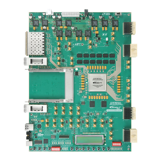
2. Board Components Introduction This chapter introduces all the important components on the Stratix V GX 100G development board. Figure 2–1 illustrates major component locations and Table 2–1 provides a brief description of all features of the board. A complete set of schematics, a physical layout database, and GERBER files for the development board reside in the Stratix V GX 100G development kit installation directory. -
Page 10: Board Overview
2–2 Chapter 2: Board Components Board Overview Board Overview This section provides an overview of the Stratix V GX 100G development board, including an annotated board image and component descriptions. Figure 2–1 provides an overview of the board features. Figure 2–1. Overview of the Stratix V GX 100G Development Board Features... - Page 11 Chapter 2: Board Components 2–3 Board Overview Table 2–1. Stratix V GX 100G Development Board Components (Part 2 of 4) Board Type Description Reference Power LED Indicates the board power status. D20-D23 Ethernet status LEDs Indicates the Ethernet connection speed as well as transmit or receive activity.
- Page 12 2–4 Chapter 2: Board Components Board Overview Table 2–1. Stratix V GX 100G Development Board Components (Part 3 of 4) Board Type Description Reference LVPECL to LVDS buffer 644.53125MHz LVDS clock buffer. U47, U48, Differential to LVDS clock Differential clock buffer (2 to 4) distributed to CMU and dedicated differential buffer clock inputs on the vertical banks of the FPGA.
- Page 13 Chapter 2: Board Components 2–5 Board Overview Table 2–1. Stratix V GX 100G Development Board Components (Part 4 of 4) Board Type Description Reference J4, J16, Interlaken interface Interlaken interface (24 channels). J38, J60 10/100/1000 Ethernet PHY Marvell 88E1111 triple speed Ethernet PHY.
-
Page 14: Featured Device: Stratix V Gx Fpga
I/O Resources Table 2–4 summarizes the FPGA I/O usage by function on the Stratix V GX 100G development board. The I/O direction is with respect to the FPGA. Table 2–4. Stratix V GX I/O Usage Summary (Part 1 of 6) - Page 15 DDR3_CK_P/_N Diff 1.5-V SSTL input DDR3 clock DDR3_CASN 1.5-V SSTL output DDR3 chip select DDR3_WEN 1.5-V SSTL output DDR3 write enable DDR3_RASN 1.5-V SSTL output DDR3 RAS# August 2012 Altera Corporation 100G Development Kit, Stratix V GX Edition Reference Manual...
- Page 16 QSFP module present QSFP_LP_MODE 2.5-V LVCMOS output QSFP low power mode SFP+ (Four each) Transceiver SFP_RD_P/_N SFP+ receive channel non-inverted/inverted input Transceiver SFP_TD_P/_N SFP+ transmit channel non-inverted/inverted output 100G Development Kit, Stratix V GX Edition August 2012 Altera Corporation Reference Manual...
- Page 17 Interlaken reference clock output (MSB) INT_MSB_CON_TX_FC_DATA 2.5-V LVCMOS output Interlaken reference clock data (MSB) INT_MSB_CON_TX_FC_SYNC 2.5-V LVCMOS output Interlaken reference clock sync (MSB) MAX II Bridge Control August 2012 Altera Corporation 100G Development Kit, Stratix V GX Edition Reference Manual...
- Page 18 2.5-V LVCMOS input 4 user push buttons LCD_CSN 2.5-V LVCMOS output LCD chip select LCD_D_CN 2.5-V LVCMOS output LCD data or control signal LCD_DATA[7:0] 2.5-V LVCMOS output LCD data 100G Development Kit, Stratix V GX Edition August 2012 Altera Corporation Reference Manual...
-
Page 19: Max Ii Cpld Epm2210 System Controller
2.5-V LVCMOS output Ethernet reset 1020 Total I/O: MAX II CPLD EPM2210 System Controller The board utilizes the EPM2210 System Controller, an Altera MAX II CPLD, for the following purposes: FPGA configuration from flash memory ■ Power consumption monitoring ■... - Page 20 Power monitor SPI input data CSENSE_SDI 2.5-V — Power monitor SPI output data CSENSE_SDO 1.5-V — Extra signal EXTRA_SIG0 1.5-V — Extra signal EXTRA_SIG1 1.5-V — Extra signal EXTRA_SIG2 100G Development Kit, Stratix V GX Edition August 2012 Altera Corporation Reference Manual...
- Page 21 BD34 FSM bus flash address FSM_A9 2.5-V AG19 FSM bus flash address FSM_A10 2.5-V AW11 FSM bus flash address FSM_A11 2.5-V AT11 FSM bus flash address FSM_A12 August 2012 Altera Corporation 100G Development Kit, Stratix V GX Edition Reference Manual...
- Page 22 MAX II CPLD on-board JTAG chain mode MAX_JTAG_TMS 2.5-V BA22 LCD display chip select LCD_CSN 2.5-V AR12 LCD data or control signal LCD_D_CN 2.5-V BB39 LCD data LCD_DATA0 2.5-V AR21 LCD data LCD_DATA1 100G Development Kit, Stratix V GX Edition August 2012 Altera Corporation Reference Manual...
- Page 23 — Power monitor control PWR_CTL 2.5-V — Chip select for the first current sense ADC SENSE_CE0 2.5-V — Chip select for the second current sense ADC SENSE_CE1 August 2012 Altera Corporation 100G Development Kit, Stratix V GX Edition Reference Manual...
- Page 24 User LED USER_LED3 2.5-V — User push button USER_PB0 2.5-V — User push button USER_PB1 2.5-V — User push button USER_PB2 2.5-V — User push button USER_PB3 100G Development Kit, Stratix V GX Edition August 2012 Altera Corporation Reference Manual...
-
Page 25: Configuration, Status, And Setup Elements
The USB-Blaster II is implemented using a USB type-B connector (J5), a USB 2.0 PHY device, and an Altera MAX II CPLD EPM570GF100 (U62). This allows configuration of the FPGA using a USB cable that connects directly between the USB port on the board (J5) and a USB port of a PC running the Quartus II software. -
Page 26: Fpga Programming From Flash Memory
.pof files (factory or user) stored in the flash. The MAX II CPLD System Controller uses the Altera Parallel Flash Loader (PFL) megafunction to configure the FPGA by reading data from the flash and converting it to FPP format. This data is then written to the FPGA’s dedicated configuration pins during configuration. -
Page 27: Status Elements
100-Mbps connection speed. Driven by the ENET_LED_LINK100 Marvell 88E1111 PHY. Green LED. Illuminates to indicate Ethernet linked 2.5-V CMOS at 10-Mbps connection speed. Driven by the ENET_LED_LINK10 Marvell 88E1111 PHY. August 2012 Altera Corporation 100G Development Kit, Stratix V GX Edition Reference Manual... - Page 28 SML-LX1206GC-TR www.lumex.com D39–D50 D11, D14, D15, D16 Green LEDs Lumex Inc. SML-LXT0805GW-TR www.lumex.com D17, D24 Red LED Lumex Inc. SML-LX1206IC-TR www.lumex.com Blue LED Lumex Inc. SML-LX1206USBC-TR www.lumex.com 100G Development Kit, Stratix V GX Edition August 2012 Altera Corporation Reference Manual...
-
Page 29: Setup Elements
Table 2–10. Board Settings DIP Switch Component References and Manufacturing Information Board Manufacturer Device Description Manufacturer Manufacturer Website Reference Part Number DIP switch Grayhill Corporation 76SB08ST www.grayhill.com August 2012 Altera Corporation 100G Development Kit, Stratix V GX Edition Reference Manual... -
Page 30: Push Buttons
Jumper removed – removes the MAX II CPLD device (U59) from the JTAG programming ■ chain. Jumper installed – fan is always on. ■ FAN BYPASS Jumper removed – MAX II CPLD EPM2210 System Controller controls the fan speed. ■ 100G Development Kit, Stratix V GX Edition August 2012 Altera Corporation Reference Manual... -
Page 31: Clock Circuitry
PLL to generate the necessary frequencies. The default frequency for the Interlaken interface is 625 MHz and for the DDR3 interface is 100 MHz. August 2012 Altera Corporation 100G Development Kit, Stratix V GX Edition Reference Manual... - Page 32 Differential programmable clock to reference clock for the LVDS AD5/AD6 PRGCLK_QL1_N/P transceivers that go to the optical interfaces. Divide-by-four differential programmable clock to the — CFP_REFCLK_N/P reference clock for the CFP interface. 100G Development Kit, Stratix V GX Edition August 2012 Altera Corporation Reference Manual...
- Page 33 100 MHz clock that goes to the MAX II System Controller — CLK_CONFIG LVCMOS for the PFL. 2.5-V 50 MHz clock that goes to the Stratix V GX and MAX II CLKIN_50_FPGA LVCMOS System Controller. August 2012 Altera Corporation 100G Development Kit, Stratix V GX Edition Reference Manual...
-
Page 34: General User Input/Output
Stratix V GX Device I/O Standard Description Reference Signal Name Pin Number 2.5-V CMOS — MAX II user push button USER_PB2 2.5-V CMOS — MAX II user push button USER_PB1 100G Development Kit, Stratix V GX Edition August 2012 Altera Corporation Reference Manual... -
Page 35: User Dip Switches
User-defined DIP switch that connects to the MAX II CPLD device. SW5.5 2.5-V CMOS — USER_DIPSW4 SW5.6 2.5-V CMOS — USER_DIPSW5 SW5.7 2.5-V CMOS — USER_DIPSW6 SW5.8 2.5-V CMOS — USER_DIPSW7 August 2012 Altera Corporation 100G Development Kit, Stratix V GX Edition Reference Manual... -
Page 36: User Leds
Signal Name Pin Number 2.5-V CMOS — USER_LED3 2.5-V CMOS — USER_LED2 General-purpose green surface mount (type 1206) user LEDs. 2.5-V CMOS — USER_LED1 2.5-V CMOS — USER_LED0 100G Development Kit, Stratix V GX Edition August 2012 Altera Corporation Reference Manual... -
Page 37: Lcd
LCD data bus 7 LCD_DATA7 2.5-V CMOS AR12 LCD data or control signal LCD_D_Cn 2.5-V CMOS AM32 LCD write enable LCD_WEn 2.5-V CMOS BA22 LCD chip select LCD_CSn August 2012 Altera Corporation 100G Development Kit, Stratix V GX Edition Reference Manual... -
Page 38: Flash Memory
Schematic Signal Stratix V GX Device I/O Standard Description Reference (U60) Name Pin Number 2.5-V CMOS AE34 Flash address valid FLASH_ADVN 2.5-V CMOS AD14 Flash chip enable FLASH_CEN 100G Development Kit, Stratix V GX Edition August 2012 Altera Corporation Reference Manual... - Page 39 2.5-V CMOS BD35 Flash data bus FSM_D3 2.5-V CMOS AV37 Flash data bus FSM_D4 2.5-V CMOS AV35 Flash data bus FSM_D5 2.5-V CMOS Flash data bus FSM_D6 August 2012 Altera Corporation 100G Development Kit, Stratix V GX Edition Reference Manual...
-
Page 40: Components And Interfaces
■ Transceiver Interfaces The Stratix V GX 100G development board includes four transceiver interfaces that utilize 46 transceiver channels. There are eight channels on the QSFP interface, four independent channels on the SFP+, 10 channels on the CFP interface, and 24 channels that make up the Interlaken interface. -
Page 41: Qsfp Interface
1.5-V PCML Transmit XCVR pair 1 from FPGA QSFP0_TX_N1 1.5-V PCML Transmit XCVR pair 2 from FPGA QSFP0_TX_P2 1.5-V PCML Transmit XCVR pair 2 from FPGA QSFP0_TX_N2 August 2012 Altera Corporation 100G Development Kit, Stratix V GX Edition Reference Manual... - Page 42 1.5-V PCML Transmit XCVR pair 0 from FPGA QSFP1_TX_P0 1.5-V PCML Transmit XCVR pair 0 from FPGA QSFP1_TX_N0 1.5-V PCML Transmit XCVR pair 1 from FPGA QSFP1_TX_P1 100G Development Kit, Stratix V GX Edition August 2012 Altera Corporation Reference Manual...
-
Page 43: Sfp+ Interface
Transmitted data (input to the SFP+ interface) SFP0_TDN 1.5-V PCML Transmitted data (input to the SFP+ interface) SFP0_TDP 2.5-V LVCMOS Turns off and disables the transmitter laser output SFP0_TXDISABLE August 2012 Altera Corporation 100G Development Kit, Stratix V GX Edition Reference Manual... - Page 44 When input signaling is high, the rate is > 4.25 GBps SFP3_RATESEL and when input signaling is low, the rate ≤ 4.25 GBps. 1.5-V PCML Received data (output from the SFP+ interface) SFP3_RDN 100G Development Kit, Stratix V GX Edition August 2012 Altera Corporation Reference Manual...
-
Page 45: Cfp Interface
CFP_MOD_LOPWR 1 or NC: Module in low-power (safe) mode Module reset. 0: Reset 2.5-V LVCMOS AH34 CFP_MOD_RST 1 or NC: Module enabled. Pull-down resistor on the module August 2012 Altera Corporation 100G Development Kit, Stratix V GX Edition Reference Manual... - Page 46 1.5-V PCML Receive XCVR pair 1 to FPGA CFP_RX_P1 1.5-V PCML Receive XCVR pair 1 to FPGA CFP_RX_N1 1.5-V PCML Receive XCVR pair 2 to FPGA CFP_RX_P2 100G Development Kit, Stratix V GX Edition August 2012 Altera Corporation Reference Manual...
- Page 47 1.5-V PCML Transmit XCVR pair 5 from FPGA CFP_TX_P5 1.5-V PCML Transmit XCVR pair 5 from FPGA CFP_TX_N5 1.5-V PCML Transmit XCVR pair 6 from FPGA CFP_TX_P6 August 2012 Altera Corporation 100G Development Kit, Stratix V GX Edition Reference Manual...
-
Page 48: Interlaken Interface
12 bits of the bus 1.5-V PCML AE41 Transmit XCVR pair 0 from FPGA INT_TX_P0 1.5-V PCML AE42 Transmit XCVR pair 0 from FPGA INT_TX_N0 100G Development Kit, Stratix V GX Edition August 2012 Altera Corporation Reference Manual... - Page 49 Receive XCVR pair 3 to FPGA INT_RX_P3 1.5-V PCML AD44 Receive XCVR pair 3 to FPGA INT_RX_N3 1.5-V PCML AY43 Receive XCVR pair 4 to FPGA INT_RX_P4 August 2012 Altera Corporation 100G Development Kit, Stratix V GX Edition Reference Manual...
- Page 50 1.5-V PCML Transmit XCVR pair 17 from FPGA INT_TX_P17 1.5-V PCML Transmit XCVR pair 17 from FPGA INT_TX_N17 1.5-V PCML Transmit XCVR pair 18 from FPGA INT_TX_P18 100G Development Kit, Stratix V GX Edition August 2012 Altera Corporation Reference Manual...
- Page 51 1.5-V PCML Receive XCVR pair 19 to FPGA INT_RX_N19 1.5-V PCML Receive XCVR pair 20 to FPGA INT_RX_P20 1.5-V PCML Receive XCVR pair 20 to FPGA INT_RX_N20 August 2012 Altera Corporation 100G Development Kit, Stratix V GX Edition Reference Manual...
-
Page 52: External Memory Interfaces
The targeted Micron device is rated at 800 MHz with a CAS latency of 11. The board will be adapted to support the 933 MHz devices from Micron as a drop in replacement once they become available. 100G Development Kit, Stratix V GX Edition August 2012 Altera Corporation Reference Manual... - Page 53 Data bus DDR3A_DQ7 1.5-V SSTL Data bus DDR3A_DQ8 1.5-V SSTL Data bus DDR3A_DQ9 1.5-V SSTL Data bus DDR3A_DQ10 1.5-V SSTL Data bus DDR3A_DQ11 1.5-V SSTL Data bus DDR3A_DQ12 August 2012 Altera Corporation 100G Development Kit, Stratix V GX Edition Reference Manual...
- Page 54 Address bus DDR3B_A1 1.5-V SSTL Address bus DDR3B_A2 1.5-V SSTL Address bus DDR3B_A3 1.5-V SSTL Address bus DDR3B_A4 1.5-V SSTL Address bus DDR3B_A5 1.5-V SSTL Address bus DDR3B_A6 100G Development Kit, Stratix V GX Edition August 2012 Altera Corporation Reference Manual...
- Page 55 Data bus DDR3B_DQ18 1.5-V SSTL Data bus DDR3B_DQ19 1.5-V SSTL Data bus DDR3B_DQ20 1.5-V SSTL Data bus DDR3B_DQ21 1.5-V SSTL Data bus DDR3B_DQ22 1.5-V SSTL Data bus DDR3B_DQ23 August 2012 Altera Corporation 100G Development Kit, Stratix V GX Edition Reference Manual...
- Page 56 Address bus DDR3C_A13 1.5-V SSTL Bank address bus DDR3C_BA0 1.5-V SSTL Bank address bus DDR3C_BA1 1.5-V SSTL Bank address bus DDR3C_BA2 1.5-V SSTL Column address select DDR3C_CASN 100G Development Kit, Stratix V GX Edition August 2012 Altera Corporation Reference Manual...
- Page 57 1.5-V SSTL Data strobe P byte lane 0 DDR3C_DQS_P0 1.5-V SSTL Data strobe N byte lane 0 DDR3C_DQS_N0 1.5-V SSTL Data strobe P byte lane 1 DDR3C_DQS_P1 August 2012 Altera Corporation 100G Development Kit, Stratix V GX Edition Reference Manual...
- Page 58 Data bus DDR3D_DQ1 1.5-V SSTL Data bus DDR3D_DQ2 1.5-V SSTL Data bus DDR3D_DQ3 1.5-V SSTL Data bus DDR3D_DQ4 1.5-V SSTL Data bus DDR3D_DQ5 1.5-V SSTL Data bus DDR3D_DQ6 100G Development Kit, Stratix V GX Edition August 2012 Altera Corporation Reference Manual...
- Page 59 DDR3D_ODT 1.5-V SSTL Row address select DDR3D_RASN 1.5-V SSTL Reset DDR3D_RSTN 1.5-V SSTL Write enable DDR3D_WEN DDR3 Port E Interface (U28, U35) 1.5-V SSTL Address bus DDR3E_A0 August 2012 Altera Corporation 100G Development Kit, Stratix V GX Edition Reference Manual...
- Page 60 Data bus DDR3E_DQ12 1.5-V SSTL Data bus DDR3E_DQ13 1.5-V SSTL Data bus DDR3E_DQ14 1.5-V SSTL Data bus DDR3E_DQ15 1.5-V SSTL Data bus DDR3E_DQ16 1.5-V SSTL Data bus DDR3E_DQ17 100G Development Kit, Stratix V GX Edition August 2012 Altera Corporation Reference Manual...
- Page 61 Address bus DDR3F_A6 1.5-V SSTL Address bus DDR3F_A7 1.5-V SSTL Address bus DDR3F_A8 1.5-V SSTL Address bus DDR3F_A9 1.5-V SSTL Address bus DDR3F_A10 1.5-V SSTL Address bus DDR3F_A11 August 2012 Altera Corporation 100G Development Kit, Stratix V GX Edition Reference Manual...
- Page 62 Data bus DDR3F_DQ23 1.5-V SSTL Data bus DDR3F_DQ24 1.5-V SSTL Data bus DDR3F_DQ25 1.5-V SSTL Data bus DDR3F_DQ26 1.5-V SSTL Data bus DDR3F_DQ27 1.5-V SSTL Data bus DDR3F_DQ28 100G Development Kit, Stratix V GX Edition August 2012 Altera Corporation Reference Manual...
-
Page 63: Qdr Ii Interface
QDRII Port A Interface (U41) 1.5-V HSTL AP24 Address bus QDR2A_A0 1.5-V HSTL AL24 Address bus QDR2A_A1 1.5-V HSTL AR23 Address bus QDR2A_A2 1.5-V HSTL BB26 Address bus QDR2A_A3 August 2012 Altera Corporation 100G Development Kit, Stratix V GX Edition Reference Manual... - Page 64 1.5-V HSTL AY31 Write data bus QDR2A_D13 1.5-V HSTL BC32 Write data bus QDR2A_D14 1.5-V HSTL AG29 Write data bus QDR2A_D15 1.5-V HSTL AH31 Write data bus QDR2A_D16 100G Development Kit, Stratix V GX Edition August 2012 Altera Corporation Reference Manual...
- Page 65 1.5-V HSTL AN27 Read data bus QDR2A_Q14 1.5-V HSTL AL28 Read data bus QDR2A_Q15 1.5-V HSTL AL27 Read data bus QDR2A_Q16 1.5-V HSTL AJ28 Read data bus QDR2A_Q17 August 2012 Altera Corporation 100G Development Kit, Stratix V GX Edition Reference Manual...
- Page 66 Address bus QDR2B_A13 1.5-V HSTL AM17 Address bus QDR2B_A14 1.5-V HSTL AL18 Address bus QDR2B_A15 1.5-V HSTL AW19 Address bus QDR2B_A16 1.5-V HSTL AJ17 Address bus QDR2B_A17 100G Development Kit, Stratix V GX Edition August 2012 Altera Corporation Reference Manual...
- Page 67 1.5-V HSTL AV13 Read data bus QDR2B_Q8 1.5-V HSTL AT14 Read data bus QDR2B_Q9 1.5-V HSTL AR14 Read data bus QDR2B_Q10 1.5-V HSTL AN15 Read data bus QDR2B_Q11 August 2012 Altera Corporation 100G Development Kit, Stratix V GX Edition Reference Manual...
-
Page 68: Gigabit Ethernet Interface
Ethernet RGMII interface. The implementation uses an auto-negotiating Marvell 88E1111 Ethernet PHY (U50) with an RGMII interface to the FPGA (using Altera Triple-Speed Ethernet MegaCore MAC function) and to a RJ-45 connector (J57) with internal magnetics that can be used for driving copper lines with Ethernet traffic. - Page 69 Media dependent interface 1 MDI_P1 2.5-V LVCMOS — Media dependent interface 1 MDI_N1 2.5-V LVCMOS — Media dependent interface 2 MDI_P2 2.5-V LVCMOS — Media dependent interface 2 MDI_N2 August 2012 Altera Corporation 100G Development Kit, Stratix V GX Edition Reference Manual...
-
Page 70: Heatsink And Fan
The board power is provided through a laptop style DC power input. The input voltage must be 19 V. The DC voltage is then stepped down to various power rails used by the components on the board. 100G Development Kit, Stratix V GX Edition August 2012 Altera Corporation Reference Manual... -
Page 71: Power Distribution System
MIC65902 VCCA_GXB Switcher Linear 0.9 V VCC, VCCHSSI, VCCHIP LTM4627 Switcher 0.75 V TPS5100 VTT, VREF Regulator 3.3 V LTM4600 5.0 V MIC49500 QSFP, SFP Switcher Linear August 2012 Altera Corporation 100G Development Kit, Stratix V GX Edition Reference Manual... -
Page 72: Power Measurement
S-PAK-7 Semiconductor Regulator - 10 A high efficiency DC/DC Linear Technology LTM4600EV#PBF www.linear.com module Micrel U37, U74 Regulator - 5 A, LDO regulator MIC69502WR www.micrel.com Semiconductor 100G Development Kit, Stratix V GX Edition August 2012 Altera Corporation Reference Manual... -
Page 73: Statement Of China-Rohs Compliance
Lead (Pb) Chromium diphenyl Ethers (Cd) (Hg) biphenyls (PBB) (Cr6+) (PBDE) Stratix V GX 100G development board 19-V power supply Type A-B USB cable User guide Notes to Table 2–42: (1) 0 indicates that the concentration of the hazardous substance in all homogeneous materials in the parts is below the relevant threshold of the SJ/T11363-2006 standard. - Page 74 2–66 Chapter 2: Board Components Statement of China-RoHS Compliance 100G Development Kit, Stratix V GX Edition August 2012 Altera Corporation Reference Manual...
- Page 75 (software licensing) Email authorization@altera.com Note to Table: (1) You can also contact your local Altera sales office or sales representative. Typographic Conventions The following table shows the typographic conventions this document uses. Visual Cue Meaning Indicate command names, dialog box titles, dialog box options, and other GUI Bold Type with Initial Capital labels.
- Page 76 Email Subscription Management Center page of the Altera website, where you can sign up to receive update notifications for Altera documents. The feedback icon allows you to submit feedback to Altera about the document. Methods for collecting feedback vary as appropriate for each document.
Need help?
Do you have a question about the Stratix V GX 100G and is the answer not in the manual?
Questions and answers