Table of Contents
Advertisement
Quick Links
Download this manual
See also:
Reference Manual
Advertisement
Table of Contents

Subscribe to Our Youtube Channel
Related Manuals for Altera Stratix V GX


Summary of Contents for Altera Stratix V GX
- Page 1 Stratix V GX FPGA Development Kit User Guide Stratix V GX FPGA Development Kit User Guide 101 Innovation Drive San Jose, CA 95134 www.altera.com UG-01103-1.2 Feedback Subscribe Downloaded from Elcodis.com electronic components distributor...
- Page 2 © 2012 Altera Corporation. All rights reserved. ALTERA, ARRIA, CYCLONE, HARDCOPY, MAX, MEGACORE, NIOS, QUARTUS and STRATIX words and logos are trademarks of Altera Corporation and registered in the U.S. Patent and Trademark Office and in other countries. All other words and logos identified as trademarks or service marks are the property of their respective holders as described at www.altera.com/common/legal.html.
-
Page 3: Table Of Contents
Stratix V GX FPGA Development Kit Installer ........ - Page 4 Default ................6–25 Stratix V GX FPGA Development Kit...
- Page 5 How to Contact Altera ........
- Page 6 Contents Stratix V GX FPGA Development Kit July 2012 Altera Corporation User Guide Downloaded from Elcodis.com electronic components distributor...
-
Page 7: Chapter 1. About This Kit
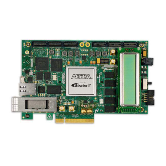
The Altera Stratix V GX FPGA Development Kit is a complete design environment that includes both the hardware and software you need to develop Stratix V GX FPGA designs. The following list describes what you can accomplish with the kit: ■... -
Page 8: Software
75 Ω SMB video cable ■ Software The software for this kit, described in the following sections, is available on the Altera website for immediate downloading. You can also request to have Altera mail the software to you on DVDs. -
Page 9: Stratix V Gx Fpga Development Kit Installer
Altera FPGA designs. Stratix V GX FPGA Development Kit Installer The license-free Stratix V GX FPGA Development Kit installer includes all the documentation and design examples for the kit. For information on installing the Development Kit Installer, refer to “Software... - Page 10 1–4 Chapter 1: About This Kit Kit Features Stratix V GX FPGA Development Kit July 2012 Altera Corporation User Guide Downloaded from Elcodis.com electronic components distributor...
-
Page 11: Chapter 2. Getting Started
Without proper anti-static handling, you can damage the board. 2. Verify that all components are on the board and appear intact. In typical applications with the Stratix V GX FPGA development board, a heat sink is not necessary. However, under extreme conditions or for engineering sample silicon the board might require additional cooling to stay within operating temperature guidelines. -
Page 12: References
2–2 Chapter 2: Getting Started References References Use the following links to check the Altera website for other related information: ■ For the latest board design files and reference designs, refer to the Stratix V GX FPGA Development Kit page. -
Page 13: Chapter 3. Software Installation
Installing the Quartus II Subscription Edition Software Included in the Quartus II Subscription Edition Software are the Quartus II software (including Qsys), the Nios II EDS, and the MegaCore IP Library. To install the Altera development tools, perform the following steps: 1. -
Page 14: Installing The Stratix V Gx Fpga Development Kit
/all at a command prompt to determine the NIC ID. Your NIC ID is the 12-digit hexadecimal number on the Physical Address line. 4. When licensing is complete, Altera emails a license.dat file to you. Store the file on your computer and use the License Setup page of the Options dialog box in the Quartus_II software to enable the software. -
Page 15: Installing The Usb-Blaster Ii Driver
Altera website. On the Altera Programming Cable Driver Information page of the Altera website, locate the table entry for your configuration and click the link to access the instructions. For USB-Blaster II configuration details, refer to the On-Board USB-Blaster II page. - Page 16 3–4 Chapter 3: Software Installation Installing the USB-Blaster II Driver Stratix V GX FPGA Development Kit July 2012 Altera Corporation User Guide Downloaded from Elcodis.com electronic components distributor...
-
Page 17: Chapter 4. Development Board Setup
4. Development Board Setup The instructions in this chapter explain how to set up the Stratix V GX FPGA development board. Setting Up the Board To prepare and apply power to the board, perform the following steps: 1. The Stratix V GX FPGA development board ships with its board switches preconfigured to support the design examples in the kit. -
Page 18: Factory Default Switch Settings
Chapter 4: Development Board Setup Factory Default Switch Settings Factory Default Switch Settings This section shows the factory switch settings for the Stratix V GX FPGA development board. Figure 4–1 shows the switch locations and the default position of each switch on the top side of the board. - Page 19 (1) Adding a single jumper between the pins sets the voltage as described in the table. Install only one jumper location at a time. July 2012 Altera Corporation Stratix V GX FPGA Development Kit User Guide Downloaded from Elcodis.com electronic components distributor...
- Page 20 (1) If you plug in an external USB-Blaster cable to the JTAG header (J10), the On Board USB-Blaster II is disabled. The JTAG chain is normally mastered by the on-board USB-Blaster II. For details on the JTAG chain, refer to the Stratix V GX FPGA Development Board Reference Manual. For USB-Blaster II configuration details, refer to the...
- Page 21 Figure 4–2. If you use an external USB Blaster, Altera recommends that you disable the power-up configuration of the FPGA by changing the MSEL(4:0) DIP switch (SW4) from 01000 to 11000. This will prevent power-up FPGA configuration from flash in the default FPPx32 mode.
- Page 22 ■ — — For more information about the FPGA board settings, refer to the Stratix V GX FPGA Development Board Reference Manual. Stratix V GX FPGA Development Kit July 2012 Altera Corporation User Guide Downloaded from Elcodis.com electronic components distributor...
-
Page 23: Chapter 5. Board Update Portal
5. Board Update Portal The Stratix V GX FPGA Development Kit ships with the Board Update Portal design example stored in the factory portion of the flash memory on the board. The design consists of a Nios II embedded processor, an Ethernet MAC, and an HTML web server. -
Page 24: Using The Board Update Portal To Update User Designs
2. In the Hardware File Name field specify the .flash file that you either downloaded from the Altera website or created on your own. If there is a software component to the design, specify it in the same manner using the Software File Name field;... -
Page 25: Chapter 6. Board Test System
6. Board Test System The kit includes design examples and an application called the Board Test System to test the functionality of the Stratix V GX FPGA development board. The application provides an easy-to-use interface to alter functional settings and observe the results. -
Page 26: Preparing The Board
BoardTestSystem.exe application. On Windows, click Start > All Programs > Altera > Stratix V GX FPGA Development Kit <version> > Board Test System to run the application. A GUI appears, displaying the application tab that corresponds to the design running in the FPGA. -
Page 27: Using The Board Test System
The following sections describe the controls on the System Info tab. Board Information The Board information control displays static information about your board. July 2012 Altera Corporation Stratix V GX FPGA Development Kit User Guide Downloaded from Elcodis.com electronic components distributor... -
Page 28: Max V Registers
MAX V ver—Indicates the version of MAX V code currently running on the board. The MAX V code resides in the <install dir>\kits\stratixVGX_5sgxea7kf40_fpga\examples directory. Newer revisions of this code might be available on the Stratix V GX FPGA Development Kit page of the Altera website. ■... -
Page 29: Jtag Chain
JTAG Chain The JTAG chain control shows all the devices currently in the JTAG chain. The Stratix V GX device is always the first device in the chain. The JTAG chain is normally mastered by the On-board USB-Blaster II. If you plug in an external USB-Blaster cable to the JTAG header (J10), the On Board USB-Blaster II is disabled. -
Page 30: The Gpio Tab
The read-only User DIP switch control displays the current positions of the switches in the user DIP switch bank (SW1). Change the switches on the board to see the graphical display change accordingly. Stratix V GX FPGA Development Kit July 2012 Altera Corporation User Guide Downloaded from Elcodis.com... -
Page 31: User Leds
The Flash tab allows you to read and write flash memory on your board. Figure 6–4 shows the Flash tab. Figure 6–4. The Flash Tab The following sections describe the controls on the Flash tab. July 2012 Altera Corporation Stratix V GX FPGA Development Kit User Guide Downloaded from Elcodis.com electronic components distributor... -
Page 32: Read
Erases flash memory, which is limited to a scratch page in the upper 128K block. Flash Memory Map Displays the flash memory map for the Stratix V GX FPGA Development Kit. Stratix V GX FPGA Development Kit July 2012 Altera Corporation... -
Page 33: The Ddr3 Tab
■ Write, Read, and Total performance bars—Show the percentage of maximum theoretical data rate that the requested transactions are able to achieve. July 2012 Altera Corporation Stratix V GX FPGA Development Kit User Guide Downloaded from Elcodis.com electronic components distributor... -
Page 34: Error Control
Write then read—Selects read and write transactions for analysis. ■ Read only—Selects read transactions for analysis. ■ Write only—Selects write transactions for analysis. Stratix V GX FPGA Development Kit July 2012 Altera Corporation User Guide Downloaded from Elcodis.com electronic components distributor... -
Page 35: The Qdrii+ Tab
The following sections describe the controls on the QDRII+ tab. Start The Start control initiates QDR II+ memory transaction performance analysis. Stop The Stop control terminates transaction performance analysis. July 2012 Altera Corporation Stratix V GX FPGA Development Kit User Guide Downloaded from Elcodis.com electronic components distributor... -
Page 36: Performance Indicators
Memory—Selects a generic data pattern stored in the on chip memory of the ■ Stratix V GX device. Math—Selects data generated from a simple math function within the FPGA ■ fabric. Stratix V GX FPGA Development Kit July 2012 Altera Corporation User Guide Downloaded from Elcodis.com electronic components distributor... -
Page 37: The Xcvr1 Tab
TX and RX PLL lanes are phase locked to data; RX lanes are word aligned and deskewed. July 2012 Altera Corporation Stratix V GX FPGA Development Kit User Guide Downloaded from Elcodis.com... -
Page 38: Port
PRBS 31—Selects pseudo-random 31-bit sequences. HF—Selects highest frequency divide-by-2 data pattern "10101010" ■ ■ HF1—Selects next highest frequency divide-by-6 data pattern "111000111000" Stratix V GX FPGA Development Kit July 2012 Altera Corporation User Guide Downloaded from Elcodis.com electronic components distributor... -
Page 39: Error Control
■ Tx (MBps) and Rx (MBps)—Show the number of bytes of data analyzed per second. July 2012 Altera Corporation Stratix V GX FPGA Development Kit User Guide Downloaded from Elcodis.com electronic components distributor... -
Page 40: The Xcvr2 Tab
Channel lock—Shows the channel locked or unlocked state. When locked, all lanes are word aligned and channel bonded, and all TX and RX PLL lanes are phase locked to data; RX lanes are word aligned and deskewed. Stratix V GX FPGA Development Kit July 2012 Altera Corporation User Guide Downloaded from Elcodis.com... -
Page 41: Port
HF—Selects highest frequency divide-by-2 data pattern "10101010" HF1—Selects next highest frequency divide-by-6 data pattern "111000111000" ■ ■ HF2—Selects second lowest frequency divide-by-22 data pattern July 2012 Altera Corporation Stratix V GX FPGA Development Kit User Guide Downloaded from Elcodis.com electronic components distributor... -
Page 42: Error Control
TX and RX performance bars—Show the percentage of maximum theoretical data rate that the requested transactions are able to achieve. ■ Tx (MBps) and Rx (MBps)—Show the number of bytes of data analyzed per second. Stratix V GX FPGA Development Kit July 2012 Altera Corporation User Guide Downloaded from Elcodis.com... -
Page 43: The Xcvr3 Tab
TX and RX PLL lanes are phase locked to data; RX lanes are word aligned and deskewed. July 2012 Altera Corporation Stratix V GX FPGA Development Kit User Guide Downloaded from Elcodis.com... -
Page 44: Port
PRBS 31—Selects pseudo-random 31-bit sequences. HF—Selects highest frequency divide-by-2 data pattern "10101010" ■ ■ HF1—Selects next highest frequency divide-by-6 data pattern "111000111000" Stratix V GX FPGA Development Kit July 2012 Altera Corporation User Guide Downloaded from Elcodis.com electronic components distributor... -
Page 45: Error Control
You can also run the Power Monitor as a stand-alone application. PowerMonitor.exe resides in the <install dir>\kits\stratixVGX_5sgxea7kf40_fpga\examples\board_test_system directory. On Windows, click Start > All Programs > Altera > Stratix V GX FPGA Development Kit <version> > Power Monitor to start the application. July 2012 Altera Corporation... -
Page 46: General Information
The Power Monitor communicates with the MAX V device on the board through the JTAG bus. A power monitor circuit attached to the MAX V device allows you to measure the power that the Stratix V GX FPGA device is consuming regardless of the design currently running. -
Page 47: Temperature Information
350 MHz must be the same frequency, and must be frequencies from 367 MHz to 473.33 MHz or from 550 MHz to 710 MHz. July 2012 Altera Corporation Stratix V GX FPGA Development Kit User Guide Downloaded from Elcodis.com... -
Page 48: Read
<install dir>\kits\stratixVGX_5sgxea7kf40_fpga\examples\board_test_system directory. On Windows, click Start > All Programs > Altera > Stratix V GX FPGA Development Kit <version> > Clock Control to start the application. For more information about the Si570, Si571, or Si5338 oscillators and the Stratix V GX FPGA development board’s clocking circuitry and clock input pins, refer to the... -
Page 49: Default
FPGA development board, power to the board is on, and no other applications that use the JTAG chain are running. To configure the Stratix V GX FPGA, perform the following steps: 1. Start the Quartus II Programmer. - Page 50 6–26 Chapter 6: Board Test System Configuring the FPGA Using the Quartus II Programmer Stratix V GX FPGA Development Kit July 2012 Altera Corporation User Guide Downloaded from Elcodis.com electronic components distributor...
-
Page 51: Cfi Flash Memory Map
A. Programming the Flash Memory Device As you develop your own project using the Altera tools, you can program the flash memory device so that your own design loads from flash memory into the FPGA on power up. This appendix describes the preprogrammed contents of the common flash... -
Page 52: Preparing Design Files For Flash Programming
If you have an FPGA design developed using the Quartus II software, and software developed using the Nios II EDS, follow these instructions: 1. On the Windows Start menu, click All Programs > Altera > Nios II EDS > Nios II Command Shell. -
Page 53: Programming Flash Memory Using The Board Update Portal
100%. The Config Done LED (D17) illuminates indicating that the flash device is ready for programming. 8. On the Windows Start menu, click All Programs > Altera > Nios II EDS > Nios II Command Shell. -
Page 54: Restoring The Flash Device To The Factory Settings
The flash device is ready for programming. 6. On the Windows Start menu, click All Programs > Altera > Nios II EDS > Nios II Command Shell. 7. In the Nios II command shell, navigate to the <install dir>\kits\stratixVGX_5sgxea7kf40_fpga\factory_recovery directory and type... -
Page 55: Restoring The Max V Cpld To The Factory Settings
To ensure that you have the most up-to-date factory restore files and information about this product, refer to the Stratix V GX FPGA Development Kit page of the Altera website. Restoring the MAX V CPLD to the Factory Settings This section describes how to restore the original factory contents to the MAX V CPLD on the FPGA development board. - Page 56 A–6 Appendix A: Programming the Flash Memory Device Restoring the MAX V CPLD to the Factory Settings Stratix V GX FPGA Development Kit July 2012 Altera Corporation User Guide Downloaded from Elcodis.com electronic components distributor...
-
Page 57: Additional Information
(software licensing) Email authorization@altera.com Note to Table: (1) You can also contact your local Altera sales office or sales representative. Typographic Conventions The following table shows the typographic conventions this document uses. Visual Cue Meaning Indicate command names, dialog box titles, dialog box options, and other GUI Bold Type with Initial Capital labels. - Page 58 Email Subscription Management Center page of the Altera website, where you can sign up to receive update notifications for Altera documents. The feedback icon allows you to submit feedback to Altera about the document. Methods for collecting feedback vary as appropriate for each document.
Need help?
Do you have a question about the Stratix V GX and is the answer not in the manual?
Questions and answers