Table of Contents
Advertisement
Quick Links
Advertisement
Table of Contents

Subscribe to Our Youtube Channel
Related Manuals for Aaeon EPIC-QM77


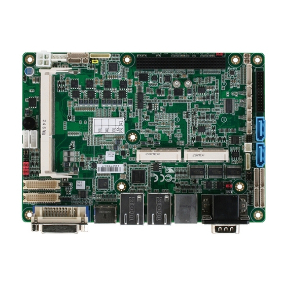
Summary of Contents for Aaeon EPIC-QM77
- Page 1 E P I C - Q M 7 7 EPIC-QM77 ® Intel Core™ i7/i5/i3/Celeron® Processor Supports DDR3/L 1333/1600 Memory 18/24-bit Single/Dual Channel LVDS CRT, DVI-I, HDMI 2 USB 3.0, 4 USB2.0, 6 COMs, 2 SATA 16-bit Digital I/O Co-lay with LPT EPIC-QM77 Manual 2nd Ed. June 9, 2014...
- Page 2 AAEON assumes no liabilities resulting from errors or omissions in this document, or from the use of the information contained herein. AAEON reserves the right to make changes in the product design without notice to its users.
- Page 3 E P I C B o a r d E P I C - Q M 7 7 Acknowledgments All other products’ name or trademarks are properties of their respective owners. Award is a trademark of Award Software International, Inc. ...
- Page 4 E P I C - Q M 7 7 Packing List Before you begin installing your card, please make sure that the following materials have been shipped: Product DVD EPIC-QM77 1702150155 SATA Power Cable 1709070500 SATA Cable M10QM77000 Heat Spreader ...
-
Page 5: Table Of Contents
E P I C B o a r d E P I C - Q M 7 7 Contents Chapter 1 General Information 1.1 Introduction ..............1-2 1.2 Features ..............1-3 1.3 Specifications ............1-4 Chapter 2 Quick Installation Guide 2.1 Safety Precautions ............ - Page 6 E P I C B o a r d E P I C - Q M 7 7 2.18 COM2 Slew Selection (JP12) ........2-16 2.19 VGA & DVI-I CONNECTOR (CN1) ......2-16 2.20 Touch Screen Connector (CN2) ......2-18 2.21 SATA Power Connector (CN3) .......
- Page 7 E P I C B o a r d E P I C - Q M 7 7 2.43 USB2.0 Connector (USB5) ........2-38 2.44 USB2.0 Connector (USB6) ........2-39 2.45 RS-232 Serial Port Dual Connector (COM1+COM2)2-39 2.46 RS-232 Serial Port Connector (COM3) ....2-41 2.47 RS-232 Serial Port Connector (COM4) ....
- Page 8 E P I C B o a r d E P I C - Q M 7 7 B.3 IRQ Mapping Chart ..........B-6 B.4 DMA Channel Assignments ......... B-11 Appendix C Mating Connector C.1 List of Mating Connectors and Cables....C-2 Appendix D Electrical Specifications for I/O Ports D.1 Electrical Specifications for I/O Ports ....
-
Page 9: Chapter 1 General Information
E P I C B o a r d E P I C - Q M 7 7 Chapter General Information 1- 1 Chapter 1 General Information... -
Page 10: Introduction
CPU and integrated Graphics support CRT/LCD simultaneous/ dual view displays. In addition to the PCI-104 expansion, EPIC-QM77 also features two SATA3, two USB 3.0 ports, four USB 2.0 ports, six COM ports, one Mini Card slot, 16-bit Digital I/O Co-lay with LPT for flexible I/O expansion. -
Page 11: Features
E P I C B o a r d E P I C - Q M 7 7 1.2 Features ® ® Intel Core™ i7/i5/i3/Celeron Processor ® Intel QM77/HM76 SODIMM DDR3/L 1333/1600MHz Memory, Max. 8GB Gigabit Ethernet x 2 ... -
Page 12: Specifications
E P I C B o a r d E P I C - Q M 7 7 1.3 Specifications System Form Factor EPIC Express Board ® ® Processor Intel Core™ i7/i5/i3/Celeron Processor System Memory 204-pin SODIMM DDR3/L 1333/1600MHz Memory, Max. - Page 13 E P I C B o a r d E P I C - Q M 7 7 Board Size 4.5" x 6.5" (115mm x 165mm) Gross Weight 0.88 lb (0.4 Kg) Operation Temperature 32°F ~ 140°F (0°C ~ 60°C) ...
- Page 14 E P I C B o a r d E P I C - Q M 7 7 supports 5/12V on D-Sub connector (COM 2) on rear I/O COM1 stack up on top of COM2; 4 COM ports on box head ...
-
Page 15: Chapter 2 Quick Installation Guide
E P I C B o a r d E P I C - Q M 7 7 Chapter Quick Installation Guide Chapter 2 Quick Installation Guide... -
Page 16: Safety Precautions
E P I C B o a r d E P I C - Q M 7 7 2.1 Safety Precautions Always completely disconnect the power cord from your board whenever you are working on it. Do not make connections while the power is on, because a sudden rush of power can damage sensitive electronic components. -
Page 17: Location Of Connectors And Jumpers
E P I C B o a r d E P I C - Q M 7 7 2.2 Location of Connectors and Jumpers Component Side Component Side Chapter 2 Quick Installation Guide... - Page 18 E P I C B o a r d E P I C - Q M 7 7 Solder Side Solder Side Chapter 2 Quick Installation Guide...
-
Page 19: Mechanical Drawing
E P I C B o a r d E P I C - Q M 7 7 2.3 Mechanical Drawing Component Side Component Side Chapter 2 Quick Installation Guide... - Page 20 E P I C B o a r d E P I C - Q M 7 7 Solder Side Solder Side Chapter 2 Quick Installation Guide...
-
Page 21: List Of Jumpers
E P I C B o a r d E P I C - Q M 7 7 2.4 List of Jumpers The board has a number of jumpers that allow you to configure your system to suit your application. The table below shows the function of each of the board's jumpers: Jumpers Label... -
Page 22: List Of Connectors
E P I C B o a r d E P I C - Q M 7 7 2.5 List of Connectors The board has a number of connectors that allow you to configure your system to suit your application. The table below shows the function of each board's connectors: Connectors Label... - Page 23 E P I C B o a r d E P I C - Q M 7 7 LAN1 1000 Base-TX Ethernet Connector LAN2 1000 Base-TX Ethernet Connector USB1 Dual USB3.0 Connector USB3 USB2.0 Connector USB4 USB2.0 Connector USB5 USB2.0 Connector USB6 USB2.0 Connector COM1(Dual A)
-
Page 24: Setting Jumpers
E P I C B o a r d E P I C - Q M 7 7 2.6 Setting Jumpers You configure your card to match the needs of your application by setting jumpers. A jumper is the simplest kind of electric switch. It consists of two metal pins and a small metal clip (often protected by a plastic cover) that slides over the pins to connect them. -
Page 25: Lpd_Dio Selection (Jp1)
E P I C B o a r d E P I C - Q M 7 7 2.7 LPD_DIO Selection (JP1) Function 2.8 AT/ATX Selection (JP2) Function 2.9 Touch Screen Selection (JP3) 4,8 Wire 5 Wire Function 5 Wire 4.8 Wire 2-11 Chapter 2 Quick Installation Guide... -
Page 26: Ring_12V_5V Selection (Jp4)
E P I C B o a r d E P I C - Q M 7 7 2.10 Ring_12V_5V Selection (JP4) +12V RI2# Function +12V RI2#_SEL 2.11 LCD VCC Selection (JP5) LVDS1 +5V LVDS1 +3.3V LVDS 1 LVDS 1 Function +5V (Default) +3.3V... -
Page 27: Lcd Backlight Voltage Selection (Jp6)
E P I C B o a r d E P I C - Q M 7 7 LVDS 2 LVDS 2 Function +5V (Default) +3.3V 2.12 LCD Backlight Voltage Selection (JP6) LVDS1 +5V LVDS1 +12V LVDS 1 LVDS 1 Function +5V (Default) +12V... -
Page 28: Lcd Backlight Control Selection (Jp7)
E P I C B o a r d E P I C - Q M 7 7 2.13 LCD Backlight Control Selection (JP7) LVDS1 Voltage-mode LVDS1 PWM-mode LVDS 1 LVDS 1 Function Voltage-mode PWM-mode LVDS2 Voltage-mode LVDS2 PWM-mode LVDS 2 LVDS 2 Function Voltage-mode... -
Page 29: Clear Cmos Selection (Jp9)
E P I C B o a r d E P I C - Q M 7 7 2.15 Clear CMOS Selection (JP9) 1 2 3 1 2 3 NORMAL CLEAR CMOS Function NORMAL CLEAR CMOS 2.16 PCI-104 I/O Voltage Selection (JP10) +3.3V JP10 Function... -
Page 30: Com2 Slew Selection (Jp12)
E P I C B o a r d E P I C - Q M 7 7 2.18 COM2 Slew Selection (JP12) 250k 1M/10M JP12 Function 250k 1M/10M 2.19 VGA & DVI-I CONNECTOR (CN1) Pin Name Signal Type Signal Level GREEN BLUE 2-16... - Page 31 E P I C B o a r d E P I C - Q M 7 7 V5S_DISP CRT_PLUG# DDC_DATA HSYNC VSYNC DDC_CLK Pin Name Signal Type Signal Level DVI_DATA2_N DVI_DATA2_P DVI_SCL DVI_SDA VSYNC DVI_DATA1_N DVI_DATA1_P V5S_DISP D_CRT_PLUG# DVI_HPD 2-17 Chapter 2 Quick Installation Guide...
-
Page 32: Touch Screen Connector (Cn2)
E P I C B o a r d E P I C - Q M 7 7 DVI_DATA0_N DVI_DATA0_P DVI_CLK_P DVI_CLK_N GREEN BLUE HSYNC 2.20 Touch Screen Connector (CN2) Pin Name Signal Type Signal Level 2-18 Chapter 2 Quick Installation Guide... -
Page 33: Sata Power Connector (Cn3)
E P I C B o a r d E P I C - Q M 7 7 SENSE 2.21 SATA Power Connector (CN3) Pin Name Signal Type Signal Level 2.22 SPI Flash Header (CN4) Pin Name Signal Type Signal Level V3.3M_SPI +3.3V SPI_CE#_F... -
Page 34: 1St Backlight Connector (Cn5)
E P I C B o a r d E P I C - Q M 7 7 SPI_SI_F 2.23 1st Backlight Connector (CN5) Pin Name Signal Type Signal Level VCC_LVDS_BKLT1 +5V OR +12V L_BRIGHTNESS1 BKLT_EN1 2.24 2nd Backlight Connector (CN6) Pin Name Signal Type Signal Level... -
Page 35: M-Sata Mini-Card Connector (Cn7)
E P I C B o a r d E P I C - Q M 7 7 BKLT_EN2 2.25 m-SATA Mini-Card Connector (CN7) Pin Name Signal Type Signal Level PCIE_WAKE# V3.3_MINICARD1 +3.3V Reserved Reserved +V1.5S +1.5V CLK_PCIE_REQ#_M PCIE Reserved Reserved CLK_PCIE_MPCIE_ Reserved... - Page 36 E P I C B o a r d E P I C - Q M 7 7 Reserved Reserved Reserved MINI_DISABLE# BUF_PLT_RST# PERn0_RX+ +V3.3_MINICARD1 +3.3V PERp0_RX- DIFF +V1.5S +1.5V SMB_CLK_SBY PETn0_TX- SMB_DATA_SBY PETp0_TX+ USB_PN2 USB_PP2 +V3.3_MINICARD1 +3.3V +V3.3_MINICARD1 +3.3V Reserved 2-22 Chapter 2 Quick Installation Guide...
-
Page 37: Pci-E Mini-Card Connector (Cn8)
E P I C B o a r d E P I C - Q M 7 7 Reserved Reserved Reserved Reserved +V1.5S +1.5V Reserved Reserved +V3.3_MINICARD1 +3.3V 2.26 PCI-E Mini-Card Connector (CN8) Pin Name Signal Type Signal Level PCIE_WAKE# +V3.3_MINICARD2 +3.3V Reserved... - Page 38 E P I C B o a r d E P I C - Q M 7 7 Reserved CLK_PCIE_MINI2_N Reserved CLK_PCIE_MINI2_P Reserved Reserved Reserved Reserved Reserved MINI_DISABLE# BUF_PLT_RST# PCIE_RXN6 +V3.3_MINICARD2 +3.3V PCIE_RXP6 +V1.5S +1.5V SMB_CLK_SBY PCIE_TNX6 SMB_DATA_SBY PCIE_TXP6 2-24 Chapter 2 Quick Installation Guide...
-
Page 39: Lpt Port Connector (Cn9)
E P I C B o a r d E P I C - Q M 7 7 USB_PN7 USB_PP7 +V3.3_MINICARD2 +3.3V +V3.3_MINICARD2 +3.3V Reserved Reserved Reserved Reserved Reserved CL_CLK +V1.5S +1.5V CL_DATA CL_RST# +V3.3_MINICARD2 +3.3V 2.27 LPT Port Connector (CN9) 2-25 Chapter 2 Quick Installation Guide... - Page 40 E P I C B o a r d E P I C - Q M 7 7 LPT Mode: Pin Name Signal Type Signal Level STOBE# #AFD PPD0 ERR# PPD1 PINIT# PPD2 SLIN# PPD3 PPD4 PPD5 PPD6 PPD7 ACK# BUSY 2-26 Chapter 2 Quick Installation Guide...
- Page 41 E P I C B o a r d E P I C - Q M 7 7 SLCT DIO Mode: Pin Name Signal Type Signal Level GPIO7 GPIO6 GPIO8 GPIO5 GPIO9 GPIO4 GPIO10 GPIO3 GPIO11 GPIO12 GPIO13 GPIO14 GPIO15 GPIO2 GPIO1 2-27...
-
Page 42: Audio Connector (Cn10)
E P I C B o a r d E P I C - Q M 7 7 GPIO0 2.28 Audio Connector (CN10) Pin Name Signal Type Signal Level MIC_L MIC_R GND_AUDIO LIN_L LIN_R GND_AUDIO LOUT_L GND_AUDIO LOUT_R +5V_AUDIO 2-28 Chapter 2 Quick Installation Guide... -
Page 43: Connector (Cn11)
E P I C B o a r d E P I C - Q M 7 7 2.29 PCI-104 Connector (CN11) 2-29 Chapter 2 Quick Installation Guide... -
Page 44: Atx 4Pin Power Connector (Cn12)
E P I C B o a r d E P I C - Q M 7 7 2.30 ATX 4Pin Power Connector (CN12) Pin Name Signal Type Signal Level +12VSB +12V +12VSB +12V 2.31 Front Panel Connector(CN13) Pin Name Signal Type Signal Level PWRSIN#... -
Page 45: Amp-R Channel Connector (Cn14)
E P I C B o a r d E P I C - Q M 7 7 2.32 AMP-R Channel Connector (CN14) Pin Name Signal Type Signal Level SPK_R+ SPK_R- 2.33 2-Pin Power Connector (CN15) Pin Name Signal Type Signal Level +12VSB +12V... -
Page 46: Amp-L Channel Connector (Cn17)
E P I C B o a r d E P I C - Q M 7 7 Pin Name Signal Type Signal Level LPC_AD0 LPC_AD1 LPC_AD2 LPC_AD3 +V3.3S +3.3V LPC_FRAME# BUF_PLT_RST# CLK_LPC_33M LPC_DRQ#0 LPC_DRQ#1 INT_SERIRQ 2.35 AMP-L Channel Connector (CN17) Pin Name Signal Type Signal Level... -
Page 47: 1St Lvds Connector (Lvds1)
E P I C B o a r d E P I C - Q M 7 7 Pin Name Signal Type Signal Level UIM_PWR +3.3V UIM_DAT UIM_CLK UIM_RST UIM_VPP 2.37 1st LVDS Connector (LVDS1) Pin Name Signal Type Signal Level BKLT_EN1 L_BRIGHTNESS1 +VDD_LVDS1... -
Page 48: 2Nd Lvds Connector (Lvds2)
E P I C B o a r d E P I C - Q M 7 7 LVDSA_DATA2 LVDSA_DATA3# LVDSA_DATA3 LVDS_DDC_DATA LVDS_DDC_CLK LVDSB_DATA0# LVDSB_DATA0 LVDSB_DATA1# LVDSB_DATA1 LVDSB_DATA2# LVDS_DATA2 LVDSB_DATA3# LVDSB_DATA3 +VDD_LVDS1 +3.3V OR +5V LVDSB_CLK# LVDSB_CLK 2.38 2nd LVDS Connector (LVDS2) Pin Name Signal Type Signal Level... - Page 49 E P I C B o a r d E P I C - Q M 7 7 +VDD_LVDS2 +3.3V OR +5V LVDSC_CLK# LVDSC_CLK +VDD_LVDS2 +3.3V OR +5V LVDSC_DATA0# LVDSC_DATA0 LVDSC_DATA1# LVDSC_DATA1 LVDSC_DATA2# LVDSC_DATA2 LVDSC_DATA3# LVDSC_DATA3 LVDS_DDC_DATA_3 LVDS_DDC_CLK_34 LVDSD_DATA0# LVDSD_DATA0 LVDSD_DATA1# LVDSD_DATA1 LVDSD_DATA2#...
-
Page 50: Fan Connector (Fan1)
E P I C B o a r d E P I C - Q M 7 7 LVDSD_CLK# LVDSD_CLK 2.39 Fan Connector (FAN1) Pin Name Signal Type Signal Level FAN_CTL FAN_TAC FAN_CTL_R 2.40 USB3.0 Dual Connector (USB1) Pin Name Signal Type Signal Level +V5A_USB_0... -
Page 51: Usb2.0 Connector (Usb3)
E P I C B o a r d E P I C - Q M 7 7 USB3_TX0_CON_N USB3_TX0_CON_P +V5A_USB_0 USBD1- USBD1+ USB3_RX1_CON_N USB3_RX1_CON_P USB3_TX1_CON_N USB3_TX1_CON_P 2.41 USB2.0 Connector (USB3) Pin Name Signal Type Signal Level +V5A_USB_2 USBD9- USBD9+ 2-37 Chapter 2 Quick Installation Guide... -
Page 52: Usb2.0 Connector (Usb4)
E P I C B o a r d E P I C - Q M 7 7 2.42 USB2.0 Connector (USB4) Pin Name Signal Type Signal Level +V5A_USB_2 USBD12- USBD12+ 2.43 USB2.0 Connector (USB5) Pin Name Signal Type Signal Level +V5A_USB_3 USBD10- USBD10+... -
Page 53: Usb2.0 Connector (Usb6)
E P I C B o a r d E P I C - Q M 7 7 2.44 USB2.0 Connector (USB6) Pin Name Signal Type Signal Level +V5A_USB_3 USBD13- USBD13+ 2.45 RS-232 Serial Port Dual Connector (COM1+COM2) COM1 (RS-232) Pin Name Signal Type Signal Level... - Page 54 E P I C B o a r d E P I C - Q M 7 7 DTR#1 DSR#1 RTS#1 CTS#1 RI#1 COM2 (RS-232) Pin Name Signal Type Signal Level DCD#2 RXD#2 TXD2 DTR#2 DSR#2 RTS#2 CTS#2 RI#2/+5V/+12V IN/PWR COM2 (RS-422) Pin Name Signal Type...
-
Page 55: Serial Port Connector (Com3)
E P I C B o a r d E P I C - Q M 7 7 NC/+5V/+12V +5V/+12V COM2 (RS-485) Pin Name Signal Type Signal Level 485D- 485D+ NC/+5V/+12V +5V/+12V 2.46 RS-232 Serial Port Connector (COM3) Pin Name Signal Type Signal Level DCD#3... -
Page 56: Serial Port Connector (Com4)
E P I C B o a r d E P I C - Q M 7 7 TXD3 CTS#3 DTR#3 RI#3 2.47 RS-232 Serial Port Connector (COM4) Pin Name Signal Type Signal Level DCD#4 DSR#4 RXD4 RTS#4 TXD4 CTS#4 DTR#4 RI#4 2-42... -
Page 57: Serial Port Connector (Com5)
E P I C B o a r d E P I C - Q M 7 7 2.48 RS-232 Serial Port Connector (COM5) Pin Name Signal Type Signal Level DCD#5 DSR#5 RXD5 RTS#5 TXD5 CTS#5 DTR#5 RI#5 2.49 RS-232 Serial Port Connector (COM6) 2-43 Chapter 2 Quick Installation Guide... -
Page 58: Battery Connector (Bat1)
E P I C B o a r d E P I C - Q M 7 7 Pin Name Signal Type Signal Level DCD#6 DSR#6 RXD6 RTS#6 TXD6 CTS#6 DTR#6 RI#6 2.50 Battery Connector (BAT1) Pin Name Signal Type Signal Level RTCBAT +3.3V... -
Page 59: Lan Ethernet Rj-45 Connector (Lan1)
E P I C B o a r d E P I C - Q M 7 7 Pin Name Signal Type Signal Level KBDATA KBCLK +V5A_KBMS MSDATA MSCLK 2.52 LAN Ethernet RJ-45 Connector (LAN1) ACT/LINK SPEED Pin Name Signal Type Signal Level LAN1_MDIP0 LAN1_MDIN0... -
Page 60: Sata Conncetor (Sata1)
E P I C B o a r d E P I C - Q M 7 7 Pin Name Signal Type Signal Level LAN2_MDIP0 LAN2_MDIN0 LAN2_MDIP1 LAN2_MDIN1 LAN2_MDIP2 LAN2_MDIN2 LAN2_MDIP3 LAN2_MDIN3 DIFF. LAN1_MDIN3 2.54 SATA CONNCETOR (SATA1) Pin Name Signal Type Signal Level SATA_TXP0... -
Page 61: Sata Conncetor (Sata2)
E P I C B o a r d E P I C - Q M 7 7 2.55 SATA CONNCETOR (SATA2) Pin Name Signal Type Signal Level SATA_TXP1 SATA_TXN1 SATA_RXN1 SATA_RXP1 2-47 Chapter 2 Quick Installation Guide... - Page 62 E P I C B o a r d E P I C - Q M 7 7 Below Table for China RoHS Requirements 产品中有毒有害物质或元素名称及含量 AAEON Main Board/ Daughter Board/ Backplane 有毒有害物质或元素 部件名称 铅 汞 镉 六价铬 多溴联苯 多溴二苯醚 (Pb)
- Page 63 I n d u s t r i a l M o t h e r b o a r d E P I C - Q M 7 7 Chapter BIOS Setup Chapter 3 AMI BIOS Setup 3-1...
-
Page 64: System Test And Initialization
4. The CMOS memory has lost power and the configuration information has been erased. The EPIC-QM77 CMOS memory has an integral lithium battery backup for data retention. However, you will need to replace the complete unit when it finally runs down. - Page 65 I n d u s t r i a l M o t h e r b o a r d E P I C - Q M 7 7 3.2 AMI BIOS Setup AMI BIOS ROM has a built-in Setup program that allows users to modify the basic system configuration.
- Page 66 I n d u s t r i a l M o t h e r b o a r d E P I C - Q M 7 7 Setup Menu Setup submenu: Main Chapter 3 AMI BIOS Setup 3-4...
- Page 67 I n d u s t r i a l M o t h e r b o a r d E P I C - Q M 7 7 Setup submenu: Advanced Options summary: ICC Spread Disabled Optimal Default, Failsafe Default Spectrum Enabled Enable Spread Spectrum function for BCLK, DMI, PEG, PCIe, PCI33, SATA, USB3.
- Page 68 I n d u s t r i a l M o t h e r b o a r d E P I C - Q M 7 7 ACPI Settings Options summary: Suspend mode S1 only (CPU Stop Clock) S3 only (Suspend to RAM) Optimal Default, Failsafe Default Select the ACPI state used for System Suspend...
- Page 69 I n d u s t r i a l M o t h e r b o a r d E P I C - Q M 7 7 Trusted Computing Options summary: Security Device Support Disable Optimal Default, Failsafe Default Enable Enable or Disables BIOS support for security device.
- Page 70 I n d u s t r i a l M o t h e r b o a r d E P I C - Q M 7 7 CPU Configuration Options summary: Hyper-Threading Disabled Enabled Optimal Default, Failsafe Default En/Disable CPU Hyper-Threading function Intel Virtualization Disabled...
- Page 71 I n d u s t r i a l M o t h e r b o a r d E P I C - Q M 7 7 Digital IO Options summary: DIO_P#1~4 Input Default Output Allows BIOS to select input/output function to corresponding DIO ping. DIO_P#5~8 Input Output...
- Page 72 I n d u s t r i a l M o t h e r b o a r d E P I C - Q M 7 7 IDE Configuration (IDE) Chapter 3 AMI BIOS Setup 3-10...
- Page 73 I n d u s t r i a l M o t h e r b o a r d E P I C - Q M 7 7 IDE Configuration (AHCI) Chapter 3 AMI BIOS Setup 3-11...
- Page 74 I n d u s t r i a l M o t h e r b o a r d E P I C - Q M 7 7 IDE Configuration (RAID) Options summary: SATA Controllers Disabled Enabled Default En/Disable SATA Controller.
- Page 75 I n d u s t r i a l M o t h e r b o a r d E P I C - Q M 7 7 AMT Configuration Options summary: Intel AMT Disabled Enabled Optimal Default, Failsafe Default En/Disable Intel Active Management Technology BIOS Extension.
- Page 76 I n d u s t r i a l M o t h e r b o a r d E P I C - Q M 7 7 USB Configuration Options summary: Legacy USB Support Enabled Optimal Default, Failsafe Default Disabled Auto Enables BIOS Support for Legacy USB Support.
- Page 77 I n d u s t r i a l M o t h e r b o a r d E P I C - Q M 7 7 F81866 Super IO Configuration Chapter 3 AMI BIOS Setup 3-15...
- Page 78 I n d u s t r i a l M o t h e r b o a r d E P I C - Q M 7 7 Serial Port 1 Configuration Options summary: Serial Port Disabled Enabled Default Allows BIOS to En/Disable correspond serial port.
- Page 79 I n d u s t r i a l M o t h e r b o a r d E P I C - Q M 7 7 Serial Port 2 Configuration Options summary: Serial Port Disabled Enabled Default Allows BIOS to En/Disable correspond serial port.
- Page 80 I n d u s t r i a l M o t h e r b o a r d E P I C - Q M 7 7 Serial Port 3 Configuration Options summary: Serial Port Disabled Enabled Default Allows BIOS to En/Disable correspond serial port.
- Page 81 I n d u s t r i a l M o t h e r b o a r d E P I C - Q M 7 7 Serial Port 4 Configuration Options summary: Serial Port Disabled Enabled Default Allows BIOS to En/Disable correspond serial port.
- Page 82 I n d u s t r i a l M o t h e r b o a r d E P I C - Q M 7 7 Serial Port 5 Configuration Options summary: Serial Port Disabled Enabled Default Allows BIOS to En/Disable correspond serial port.
- Page 83 I n d u s t r i a l M o t h e r b o a r d E P I C - Q M 7 7 Serial Port 6 Configuration Options summary: Serial Port Disabled Enabled Default Allows BIOS to En/Disable correspond serial port.
- Page 84 I n d u s t r i a l M o t h e r b o a r d E P I C - Q M 7 7 Parallel Port Configuration Options summary: Parallel Port Disabled Enabled Default Allows BIOS to En/Disable Parallel port.
- Page 85 I n d u s t r i a l M o t h e r b o a r d E P I C - Q M 7 7 F81866 H/W Monitor Options summary: Smart Fan Function Disabled Enabled Default Enable or Disable Smart Fan.
- Page 86 I n d u s t r i a l M o t h e r b o a r d E P I C - Q M 7 7 Smart Fan Mode Configuration (Auto Duty-Cycle Mode) Chapter 3 AMI BIOS Setup 3-24...
- Page 87 I n d u s t r i a l M o t h e r b o a r d E P I C - Q M 7 7 Smart Fan Mode Configuration (Manual Duty Mode) Chapter 3 AMI BIOS Setup 3-25...
- Page 88 I n d u s t r i a l M o t h e r b o a r d E P I C - Q M 7 7 Smart Fan Mode Configuration (Manual RPM Mode) Options summary: Manual Duty Mode Fan 1 Smart Fan Control Auto RPM Mode Auto Duty-Cycle Mode Default...
- Page 89 I n d u s t r i a l M o t h e r b o a r d E P I C - Q M 7 7 Setup submenu: Chipset Chapter 3 AMI BIOS Setup 3-27...
- Page 90 I n d u s t r i a l M o t h e r b o a r d E P I C - Q M 7 7 PCH-IO Configuration Options summary: Mini Card2 Controller Disabled Enabled Default Control the PCI Express Root Port.
- Page 91 I n d u s t r i a l M o t h e r b o a r d E P I C - Q M 7 7 Enabled Default Control the PCI Express Root Port Azalia Disabled Enabled Auto Default...
- Page 92 I n d u s t r i a l M o t h e r b o a r d E P I C - Q M 7 7 System Agent (SA) Configuration Options summary: VT-d Disabled Enabled Default Check to enable VT-d function on MCH Chapter 3 AMI BIOS Setup 3-30...
- Page 93 I n d u s t r i a l M o t h e r b o a r d E P I C - Q M 7 7 Graphics Configuration Options summary: Primary Display Auto Default IGFX Select which of IGFX/PEG/PCI Graphics device should be Primary Display or select SG for Switchable Gfx.
- Page 94 I n d u s t r i a l M o t h e r b o a r d E P I C - Q M 7 7 DVMT Pre-Allocated 32MB 64MB Default 96MB 128MB 160MB 192MB 224MB 256MB 288MB 320MB...
- Page 95 I n d u s t r i a l M o t h e r b o a r d E P I C - Q M 7 7 LCD Control Options summary: Primary Display VBIOS Default Default LVDS HDMI Select the Video Device which will be activated during POST.
- Page 96 I n d u s t r i a l M o t h e r b o a r d E P I C - Q M 7 7 Internal-LVDS LCD Panel Type 640x 480 18Bit 800x 480 18Bit 800x 600 18Bit 1024x 768 18Bit Default...
- Page 97 I n d u s t r i a l M o t h e r b o a r d E P I C - Q M 7 7 Memory Information Chapter 3 AMI BIOS Setup 3-35...
- Page 98 I n d u s t r i a l M o t h e r b o a r d E P I C - Q M 7 7 Setup submenu: Boot Options summary: Quiet Boot Disabled Enabled Default En/Disable showing boot logo.
- Page 99 I n d u s t r i a l M o t h e r b o a r d E P I C - Q M 7 7 BBS Priorities Chapter 3 AMI BIOS Setup 3-37...
- Page 100 I n d u s t r i a l M o t h e r b o a r d E P I C - Q M 7 7 Security Change User/Supervisor Password You can install a Supervisor password, and if you install a supervisor password, you can then install a user password.
- Page 101 I n d u s t r i a l M o t h e r b o a r d E P I C - Q M 7 7 Setup submenu: Exit Chapter 3 AMI BIOS Setup 3-39...
-
Page 102: Chapter 4 Driver Installation
E P I C B o a r d E P I C - Q M 7 7 Chapter Driver Installation 4 - 1 Chapter 4 Driver Installation... - Page 103 E P I C B o a r d E P I C - Q M 7 7 The EPIC-QM77 comes with a DVD-ROM that contains all drivers and utilities that meet your needs. Follow the sequence below to install the drivers: Step 1 –...
- Page 104 E P I C B o a r d E P I C - Q M 7 7 4.1 Installation: Insert the EPIC-QM77 DVD-ROM into the DVD-ROM Drive. And install the drivers from Step 1 to Step 9 in order. Step 1 – Install Chipset Driver 1.
- Page 105 E P I C B o a r d E P I C - Q M 7 7 Step 3 – Install LAN (Intel_82579) Driver 1. Click on the STEP3-LAN (Intel_82579) folder and select the OS folder your system is 2.
- Page 106 E P I C B o a r d E P I C - Q M 7 7 Step 7 – Install TPM Driver 1. Click on the STEP7-TPM folder and select the OS folder your system is 2. Double click on the Setup.exe file located in each OS folder 3.
-
Page 107: Appendix A Programming The Watchdog Timer
E P I C B o a r d E P I C - Q M 7 7 Appendix Programming the Watchdog Timer Appendix A Programming the Watchdog Timer A-1... -
Page 108: Watchdog Timer Initial Program
E P I C B o a r d E P I C - Q M 7 7 A.1 Watchdog Timer Initial Program Table 1 : SuperIO relative register table Default Value Note SIO MB PnP Mode Index Register Index 0x2E (Note1) 0x2E or 0x4E SIO MB PnP Mode Data Register Data 0x2F (Note2) 0x2F or 0x4F Table 2 : Watchdog relative register table ... - Page 109 E P I C B o a r d E P I C - Q M 7 7 ************************************************************************************ // SuperIO relative definition (Please reference to Table 1) #define byte SIOIndex //This parameter is represented from Note1 #define byte SIOData //This parameter is represented from Note2 #define void IOWriteByte(byte IOPort, byte Value); #define byte IOReadByte(byte IOPort); // Watch Dog relative definition (Please reference to Table 2) ...
- Page 110 E P I C B o a r d E P I C - Q M 7 7 ************************************************************************************ Main VOID (){ // Procedure : AaeonWDTConfig // (byte)Timer : Time of WDT timer.(0x00~0xFF) // (boolean)Unit : Select time unit(0: second, 1: minute). AaeonWDTConfig(); // Procedure : AaeonWDTEnable // This procudure will enable the WDT counting. AaeonWDTEnable(); } ************************************************************************************ Appendix A Programming the Watchdog Timer A-4...
- Page 111 E P I C B o a r d E P I C - Q M 7 7 ************************************************************************************ // Procedure : AaeonWDTEnable AaeonWDTEnable () VOID { WDTEnableDisable( ); EnableLDN, EnableReg, EnableBit, 1 } // Procedure : AaeonWDTConfig AaeonWDTConfig () VOID { // Disable WDT counting WDTEnableDisable( ); EnableLDN, EnableReg, EnableBit, 0 // Clear Watchdog Timeout Status WDTClearTimeoutStatus(); // WDT relative parameter setting ...
- Page 112 E P I C B o a r d E P I C - Q M 7 7 ************************************************************************************ SIOEnterMBPnPMode() VOID { IOWriteByte(SIOIndex, 0x87); IOWriteByte(SIOIndex, 0x87); } SIOExitMBPnPMode() VOID { IOWriteByte(SIOIndex, 0xAA); } SIOSelectLDN(byte LDN) VOID { ...
-
Page 113: Appendix B I/O Information
E P I C B o a r d E P I C - Q M 7 7 Appendix I/O Information Appendix B I/O Information... -
Page 114: I/O Address Map
E P I C B o a r d E P I C - Q M 7 7 B.1 I/O Address Map Appendix B I/O Information... - Page 115 E P I C B o a r d E P I C - Q M 7 7 Appendix B I/O Information...
- Page 116 E P I C B o a r d E P I C - Q M 7 7 Appendix B I/O Information...
-
Page 117: Memory Address Map
E P I C B o a r d E P I C - Q M 7 7 B.2 Memory Address Map Appendix B I/O Information... - Page 118 E P I C B o a r d E P I C - Q M 7 7 B.3 IRQ Mapping Chart Appendix B I/O Information...
- Page 119 E P I C B o a r d E P I C - Q M 7 7 Appendix B I/O Information...
- Page 120 E P I C B o a r d E P I C - Q M 7 7 Appendix B I/O Information...
- Page 121 E P I C B o a r d E P I C - Q M 7 7 Appendix B I/O Information...
- Page 122 E P I C B o a r d E P I C - Q M 7 7 B-10 Appendix B I/O Information...
- Page 123 E P I C B o a r d E P I C - Q M 7 7 B.4 DMA Channel Assignments B-11 Appendix B I/O Information...
- Page 124 E P I C B o a r d E P I C - Q M 7 7 Appendix Mating Connector C - 1 Appendix C Mating Connector...
- Page 125 E P I C B o a r d E P I C - Q M 7 7 C.1 List of Mating Connectors and Cables The table notes mating connectors and available cables. Connector Function Mating Connector Available Cable P/N Label Cable Vendor Model number...
- Page 126 E P I C B o a r d E P I C - Q M 7 7 USB2.0 PINREX 712-75-05W001 1700050207 USB4 Connector USB2.0 PINREX 712-75-05W001 1700050207 USB5 Connector USB2.0 PINREX 712-75-05W001 1700050207 USB6 Connector COM3 PINREX 712-75-09W001 1701090150 RS-232 COM3 Serial Port...
- Page 127 E P I C B o a r d E P I C - Q M 7 7 A ppendix Electrical Specifications for I/O Ports Appendix D Electrical Specifications for I/O Ports...
-
Page 128: D.1 Electrical Specifications For I/O Ports
E P I C B o a r d E P I C - Q M 7 7 D.1 Electrical Specifications for I/O Ports Reference Signal Name Rate Output +3.3V/1A or LVDS Port 1 LVDS1 +5V/1A +3.3V/1A or LVDS Port 2 LVDS2 +5V/1A LPC Port... -
Page 129: D.2 Dio Programming
E P I C B o a r d E P I C - Q M 7 7 D.2 DIO Programming EPIC-QM77 utilizes FINTEK 81866 chipset as its Digital I/O controller. Below are the procedures to complete its configuration and the AAEON initial watchdog timer program is also attached based on which you can develop customized program to fit your application. -
Page 130: D.3 Digital I/O Register
E P I C B o a r d E P I C - Q M 7 7 D.3 Digital I/O Register Table 1 : SuperIO relative register table Default Value Note SIO MB PnP Mode Index Register Index 0x2E (Note1) 0x2E or 0x4E SIO MB PnP Mode Data Register Data 0x2F (Note2) 0x2F or 0x4F Table 2 : Digital Input relative register table LDN Register ... - Page 131 E P I C B o a r d E P I C - Q M 7 7 Table 3 : Digital Output relative register table LDN Register BitNum Value Note PE DIO‐1 Output Data 0x06 0x88 (Note27) (Note28) (Note29) (Note30) BUSY DIO‐2 Output Data 0x06 0x88 ...
-
Page 132: D.4 Digital I/O Sample Program
E P I C B o a r d E P I C - Q M 7 7 D.4 Digital I/O Sample Program ************************************************************************************ // SuperIO relative definition (Please reference to Table 1) #define byte SIOIndex //This parameter is represented from Note1 #define byte SIOData //This parameter is represented from Note2 #define void IOWriteByte(byte IOPort, byte Value); #define ... - Page 133 E P I C B o a r d E P I C - Q M 7 7 ************************************************************************************ // Digital Output control relative definition (Please reference to Table 3) #define byte DOutput1LDN // This parameter is represented from Note27 #define byte DOutput1Reg // This parameter is represented from Note28 #define byte DOutput1Bit // This parameter is represented from Note29 #define byte DOutput1Val // This parameter is represented from Note30 #define byte ...
- Page 134 E P I C B o a r d E P I C - Q M 7 7 ************************************************************************************ // Digital Input Status relative definition (Please reference to Table 2) #define byte DInput11LDN // This parameter is represented from Note3‐1 #define byte DInput11Reg // This parameter is represented from Note4‐1 #define byte DInput11Bit // This parameter is represented from Note5‐1 #define byte DInput12LDN // This parameter is represented from Note6‐1 #define byte ...
- Page 135 E P I C B o a r d E P I C - Q M 7 7 ************************************************************************************ // Digital Output control relative definition (Please reference to Table 3) #define byte DOutput11LDN // This parameter is represented from Note27‐1 #define byte DOutput11Reg // This parameter is represented from Note28‐1 #define byte DOutput11Bit // This parameter is represented from Note29‐1 #define byte DOutput11Val // This parameter is represented from Note30‐1 #define byte ...
- Page 136 E P I C B o a r d E P I C - Q M 7 7 ************************************************************************************ Main VOID (){ Boolean PinStatus ; // Procedure : AaeonReadPinStatus // Input : // Example, Read Digital I/O Pin 3 status // Output : // InputStatus : // 0: Digital I/O Pin level is low // ...
- Page 137 E P I C B o a r d E P I C - Q M 7 7 ************************************************************************************ AaeonReadPinStatus(byte LDN, byte Register, byte BitNum) Boolean { Boolean PinStatus ; PinStatus = SIOBitRead(LDN, Register, BitNum); Return PinStatus ; } AaeonSetOutputLevel(byte LDN, byte Register, byte BitNum, byte Value) VOID { ConfigToOutputMode(LDN, Register, BitNum); SIOBitSet(LDN, Register, BitNum, Value); ************************************************************************************ D-11 Appendix D Electrical Specifications for I/O Ports...
- Page 138 E P I C B o a r d E P I C - Q M 7 7 ************************************************************************************ SIOEnterMBPnPMode() VOID { IOWriteByte(SIOIndex, 0x87); IOWriteByte(SIOIndex, 0x87); } SIOExitMBPnPMode() VOID { IOWriteByte(SIOIndex, 0xAA); } SIOSelectLDN(byte LDN) VOID { ...
- Page 139 E P I C B o a r d E P I C - Q M 7 7 ************************************************************************************ SIOBitRead(byte LDN, byte Register, byte BitNum) Boolean { Byte TmpValue; SIOEnterMBPnPMode(); SIOSelectLDN(LDN); IOWriteByte(SIOIndex, Register); TmpValue = IOReadByte(SIOData); TmpValue &= (1 << BitNum); SIOExitMBPnPMode(); If(TmpValue == 0) Return 0; ...
Need help?
Do you have a question about the EPIC-QM77 and is the answer not in the manual?
Questions and answers