Table of Contents
Advertisement
Quick Links
Advertisement
Table of Contents

Related Manuals for Motorola MVME761-001


Summary of Contents for Motorola MVME761-001
- Page 1 MVME761 Transition Module Installation and Use VME761A/IH4 May 14, 1999...
- Page 2 While reasonable efforts have been made to assure the accuracy of this document, Motorola, Inc. assumes no liability resulting from any omissions in this document, or from the use of the information obtained therein. Motorola reserves the right to revise this document and to make changes from time to time in the content hereof without obligation of Motorola to notify any person of such revision or changes.
- Page 3 Preface MVME761 Transition Module Installation and Use provides general information, hardware preparation, installation instructions and support information for the MVME761-001 and MVME761-011 Transition Modules. The MVME761-0x1 Transition Module is used as the interface between the following host VMEmodules and various peripheral devices:...
-
Page 4: Related Documentation
V36V46A/PG Reference Guide Each Motorola Computer Group manual publication number is suffixed with characters that represent the revision level of the document, such as /IH2 (second revision). To obtain the most up-to-date product information in PDF or HTML format, visit our Web site at http://www.mcg.mot.com/literature. - Page 5 The safety precautions listed below represent warnings of certain dangers of which Motorola is aware. You, as the user of the product, should follow these warnings and all other safety precautions necessary for the safe operation of the equipment in your operating environment.
- Page 6 A proper installation in a CE-marked system will maintain the required EMC/safety performance. ® Motorola and the Motorola symbol are registered trademarks of Motorola, Inc. All other products mentioned in this document are trademarks or registered trademarks of their respective holders. © Copyright Motorola 1998, 1999...
-
Page 7: Table Of Contents
General Information Introduction........................1-1 Product Overview.......................1-1 Features ........................1-1 General Description ....................1-2 Serial Port Interface Modules ..................1-4 P2 Adapter Boards .....................1-5 Three-row P2 adapter (MVME761-001) ............1-5 Five-Row P2 adapter (MVME761-011) .............1-6 Connectors and Cables....................1-7 Specifications ......................1-9 Cooling requirements..................1-9 FCC compliance ....................1-9 CHAPTER 2 Hardware Preparation and Installation Introduction........................2-1... - Page 8 CHAPTER 4 Connector Pin Assignments Introduction ....................... 4-1 MVME761 Transition Module Connectors............... 4-1 P2 connector ....................... 4-1 Asynchronous serial port connectors (J5/J6)............4-3 Asynchronous/Synchronous serial port connectors (J7/J8)........ 4-4 Parallel I/O port connector (J4) ................4-6 Ethernet Connector (J9)..................4-7 P2 Adapter Connectors....................
- Page 9 List of Figures Figure 1-1. MVME761 transition module front panel and component side....1-3 Figure 1-2. 3-row DIN backplane P2 adapter (MVME761-001).......1-5 Figure 1-3. 5-row DIN backplane P2 adapter (MVME761-011).......1-6 Figure 2-1. Serial port interface jumper settings............2-2 Figure 2-2. Serial interface module and connector P1..........2-3 Figure 2-3.
- Page 10 List of Tables Table 1-1. SIM part numbers ..................1-4 Table 1-2. MVME761 transition module connectors..........1-7 Table 1-3. 3-Row P2 adapter connectors (MVME761-001) ........1-7 Table 1-4. 5-Row P2 adapter connectors (MVME761-011) ........1-8 Table 1-5. MVME761 transition module cables ............1-8 Table 1-6. MVME761-0x1 specifications ..............1-9 Table 3-1.
-
Page 11: Introduction
1General Information Introduction This manual provides general information, hardware preparation, installation instructions, and a functional description for the MVME761-001 and MVME761-011 Transition Modules. Product Overview The MVME761-0x1 Transition Module provides the interface between the MVME260x, MVME270x, MVME360x, or MVME460x Single Board Computer VMEmodule and various peripheral devices. -
Page 12: General Description
Both MVME761-0x1 models use the same transition module. The MVME761-001 comes with a P2 adapter that connects to a 3-row DIN chassis backplane. The MVME761-011 comes with a P2 adapter that connects to a 5-row DIN chassis backplane. -
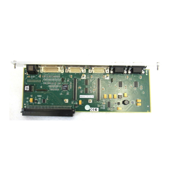
Page 13: Figure 1-1. Mvme761 Transition Module Front Panel And Component Side
General Description MVME 761-001 Figure 1-1. MVME761 transition module front panel and component side http://www.mcg.mot.com/literature... -
Page 14: Serial Port Interface Modules
V.35 DTE SIMV35DTE 01-W3127F01A X.21 DCE SIMX21DCE 01-W3167F01B X.21 DTE SIMX21DTE 01-W3166F01A Note Additional SIMs may be released. Please see your Motorola representative for a complete list of SIMS that are available for the MVME761-0x1. Computer Group Literature Center Web Site... -
Page 15: P2 Adapter Boards
Ethernet signals to the MVME761 transition module. Three-row P2 adapter (MVME761-001) The P2 adapter for the MVME761-001 mounts onto a 3-row, 96-pin P2 backplane connector. The 50-pin male connector, J2, carries the 8-bit SCSI signals from the MVME260x, MVME270x, MVME360x, or MVME460x. -
Page 16: Five-Row P2 Adapter (Mvme761-011)
General Information Five-Row P2 adapter (MVME761-011) The P2 adapter for the MVME761-011 mounts onto a 5-row, 160-pin P2 backplane connector. The 68- pin female connector, J1, carries 16-bit SCSI signals from the MVME260x, MVME270x, MVME360x, or MVME460x. It also has a 64-pin male connector, J3, for PMC I/O. 1999 9701 Figure 1-3. -
Page 17: Connectors And Cables
8-pin female RJ-45 Ethernet port connector 100Base-TX J1, J12 60-pin female connector 64-pin male connector to J2 on the P2 adapter Table 1-3. 3-Row P2 adapter connectors (MVME761-001) Type Number Description 96-pin female DIN 41612 connector to the chassis backplane... -
Page 18: Table 1-4. 5-Row P2 Adapter Connectors (Mvme761-011)
General Information Table 1-4. 5-Row P2 adapter connectors (MVME761-011) Type Number Description 160-pin female DIN 41612 connector to the chassis backplane 64-pin male connector for output to P2 on the transition module MVME761 PMC I/O 64-pin male connector for PMC I/O SCSI 68-pin female IDC connector for internal SCSI devices Table 1-5. -
Page 19: Specifications
Specifications Specifications The MVME761 transition module specifications are shown in Table 1-6. Table 1-6. MVME761-0 x 1 specifications Characteristics Specifications Power Requirements +12Vdc, 100mA typical, 200mA maximum -12Vdc, 100mA (for some of the SIMs) Operating temperature to 55 C at chassis point of entry of forced air (approximately 5 CFM) Storage temperature to +85... -
Page 20: Introduction
The MVME761-0x1 is packed in an antistatic wrapper to protect it from Use ESD static discharge. Motorola strongly recommends that you use an antistatic wrist strap and a conductive foam pad when handling the equipment. Electronic components can be extremely sensitive to electrostatic discharge (ESD). -
Page 21: Installing The Serial Interface Modules
Hardware Preparation and Installation Installing the Serial Interface Modules Configure the serial ports 3 and 4 for the required interface by installing the appropriate SIM. See Table 1-1 on page 1-4 for a list of the serial port interface types. Prior to installing the SIMs, set the jumpers on header J2 (for serial port 3) and header J3 (for serial port 4) for either DCE or DTE. -
Page 22: Figure 2-2. Serial Interface Module And Connector P1
Installing the Serial Interface Modules Mounting Hole Alignment Mounting Hole 11637 9610 Figure 2-2. Serial interface module and connector P1 2. Place the SIM onto the transition module SIM connector, making sure that the mounting holes also line up with the standoffs on the transition module as shown in Figure 2-3. -
Page 23: Figure 2-3. Installing A Sim Onto The Mvme761 Transition Module
Hardware Preparation and Installation 1911 9609 Figure 2-3. Installing a SIM onto the MVME761 transition module Computer Group Literature Center Web Site... -
Page 24: Installing The Transition Module And P2 Adapter
The P2 adapter is required because the P2 connector on the transition module is not compatible with the P2 connector on the chassis backplane. Motorola strongly recommends that you use an antistatic wrist strap and a Use ESD conductive foam pad when installing boards in a system chassis. -
Page 25: Procedure
Hardware Preparation and Installation VME BACKPLANE MVME761 Transition Module MVME260 x /MVME360 x 30-W2799B02A 64-CONDUCTOR CABLE P2 ADAPTER J3 ON THE 3-ROW P2 ADAPTER J4 ON THE 5-ROW P2 ADAPTER ENCLOSURE BOUNDARY 11654.00 9610 Figure 2-4. MVME761-0 x 1 chassis connections Procedure 1. - Page 26 Installing the Transition Module and P2 Adapter 4. If necessary, move some of the other modules to allow space for the cables connected to the P2 adapter and the transition module. 5. Install the jumper on header J1 (on the 3-row P2 adapter or header J5 on the 5-row P2 adapter) if you are supporting SCSI devices.
-
Page 27: Introduction
3Functional Description Introduction This chapter provides information on MVME761 transition module and SIM circuitry, P2 signal multiplexing, and the configuration of the serial ports. Circuitry The MVME761 transition module and the Serial Interface Modules (SIMs) convert the TTL level signals to and from the MVME260x, MVME270x, MVME360x, and MVME460x modules to the reception and transmission levels specified by the appropriate port interface standard. -
Page 28: Figure 3-1. Mvme761 Transition Module Block Diagram
Functional Description 10Base-T Parallel COM1 COM2 Serial 3 Serial 4 100Base-TX Serial Interface Serial Interface Module (SIM) Module (SIM) Buffers EIA-232-D P2 Multiplex Function 64-Pin DIN Connector 11638.00 9611 Figure 3-1. MVME761 transition module block diagram Computer Group Literature Center Web Site... -
Page 29: Figure 3-2. 3-Row Din Backplane P2 Adapter Block Diagram
Circuitry 8-bit Single-ended SCSI 64-pin Connector to MVME761 Transition Module SCSI Terminators 3-Row Backplane Connector 11639.00 9611 Figure 3-2. 3-Row DIN backplane P2 adapter block diagram 16-bit Single-ended SCSI 64-pin Connector to MVME761 Transition Module SCSI PMC I/O Terminators 5-Row Backplane Connector 11752.00 9703 Figure 3-3. -
Page 30: P2 Signal Multiplexing (P2Mx)
Functional Description P2 Signal Multiplexing (P2MX) Because of a limited number of pins on the P2 connector, both the VME processor board and the MVME761 transition module multiplex and de- multiplex some of the P2 signals. This function, called P2MX is transparent to the software and the user. - Page 31 P2 Signal Multiplexing (P2MX) Table 3-1. P2 signal multiplexing sequence MXDO MXDI (from the (from the MVME761) MVME260x/MVME270x/MVME360x/ MVME460x) Time Slot Signal Name Time Slot Signal Name Reserved DSR1 Reserved DCD1 Reserved Reserved DSR2 Reserved DCD2 MXCLK is the 10MHz bit clock for the time-multiplexed data lines, MXDO and MXDI.
-
Page 32: Figure 3-4. Multiplex Signal Timing Chart
Functional Description Time Slot 1 Time Slot 2 Time Slot 15 Time Slot 0 Time Slot 3 MXCLK MXSYNC# MXDO Reserved RTS3 DTR3 LLB3 RLB3 MXDI DCD2 CTS3 DSR3 DCD3 11640.00 9611 Figure 3-4. Multiplex signal timing chart Computer Group Literature Center Web Site... -
Page 33: Serial Interface Module Circuitry
Serial Interface Module Circuitry Serial Interface Module Circuitry Each Serial Interface Module has a 60-pin connector that provides all signal and power connections to the MVME761 transition module. TTL-level signals All TTL-level signals, with the exception of data and clocks, are active low. -
Page 34: Port Configuration Diagrams
Functional Description For all port interfaces, the SIMs support the transmitter signal element timing as either input or output signals. Port Configuration Diagrams COM1 and COM2 asynchronous serial ports The asynchronous serial port (COM1 and COM2) configuration is shown Figure 3-5. -
Page 35: Figure 3-5. Eia-574 Dte Port Configuration (Com1 And Com2)
Port Configuration Diagrams SOUT1 RTS1# DTR1# SIN1 COM1 CTS1# DSR1# DCD1# RI1# PC87308 P2/P2MX SOUT2 RTS2# DTR2# SIN2 COM2 CTS2# DSR2# DCD2# RI2# MVME260 X/ MVME761 MVME360 X Transition Module Figure 3-5. EIA-574 DTE port configuration (COM1 and COM2) http://www.mcg.mot.com/literature... -
Page 36: Asynchronous/Synchronous Serial Ports
Functional Description Asynchronous/Synchronous Serial Ports The asynchronous/synchronous serial port (Port 3 and Port 4) interface configuration diagrams are on the following pages. 3-10 Computer Group Literature Center Web Site... -
Page 37: Figure 3-6. Mvme761 Eia232 Dce Configuration Port 3
Port Configuration Diagrams MVME761 VME MODULE Z85230 SCC HD26 EIA232-DCE SIM RTS# CTS# DCD# TRXC RTXC P2/P2MX Z8536 CIO DTR# LLB# RLB# DSR# Header J18 1-2 Header J2 2-3 11552 9902 (2-5) Figure 3-6. MVME761 EIA232 DCE configuration port 3 http://www.mcg.mot.com/literature 3-11... -
Page 38: Figure 3-7. Mvme761 Eia232 Dce Configuration Port 4
Functional Description VME MODULE MVME761 Z85230 SCC HD26 EIA232-DCE SIM RTS# CTS# DCD# TRXC RTXC P2/P2MX Z8536 CIO DTR# LLB# RLB# DSR# Headers: J16 2-3 Header J3 2-3 J17 1-2 J19 1-2 11552 9902 (3-5) Figure 3-7. MVME761 EIA232 DCE configuration port 4 3-12 Computer Group Literature Center Web Site... -
Page 39: Figure 3-8. Mvme761 Eia232-Dte Configuration Port 3
Port Configuration Diagrams VME MODULE MVME761 Z85230 SCC HD26 EIA232-DTE SIM RTS# CTS# DCD# TRXC RTXC P2/P2MX Z8536 CIO DTR# LLB# RLB# DSR# Header J18 2-3 Header J2 1-2 11552 9902(4-5) Figure 3-8. MVME761 EIA232-DTE configuration port 3 http://www.mcg.mot.com/literature 3-13... -
Page 40: Figure 3-9. Mvme761 Eia232-Dte Configuration Port 4
Functional Description MVME761 VME MODULE Z85230 SCC HD26 EIA232-DTE SIM RTS# CTS# DCD# TRXC RTXC P2/P2MX Z8536 CIO DTR# LLB# RLB# DSR# Headers: J16 2-3 Header J3 1-2 J17 2-3 J19 1-2 11552 9902 (5-5) Figure 3-9. MVME761 EIA232-DTE configuration port 4 3-14 Computer Group Literature Center Web Site... -
Page 41: Figure 3-10. Mvme761 Eia530-Dce Configuration Port 3
Port Configuration Diagrams MVME761 VME MODULE DB26 Z85230 SCC EIA530-DCE SIM RXDB RXDA CTSB RTS# CTSA TXDB TXDA RTSB CTS# RTSA DTRB DCD# DTRA TXCB TRXC TXCA RXCB RXCA ETXCB P2/P2MX RTXC ETXCA Z8536 CIO DCDB DTR# DCDA LLB# RLB# DSRB DSR# DSRA... -
Page 42: Figure 3-11. Mvme761 Eia530-Dce Configuration Port 4
Functional Description MVME761 VME MODULE DB26 Z85230 SCC EIA-530 DCE SIM RXDB RXDA CTSB RTS# CTSA TXDB TXDA RTSB CTS# RTSA DTRB DCD# DTRA TXCB TXCA RXCB RXCA TRXC ETXCB ETXCA RTXC P2/P2MX Z8536 CIO DCDB DTR# DCDA LLB# RLB# DSRB DSR# DSRA... -
Page 43: Figure 3-12. Mvme761 Eia530-Dte Configuration Port 3
Port Configuration Diagrams MVME761 VME MODULE DB26 Z85230 SCC EIA530-DTE SIM TXDB TXDA RTSB RTS# RTSA RXDB RXDA CTSB CTS# CTSA DTRB DCD# DTRA ETXCB TRXC ETXCA TXCB TXCA RXCB P2/P2MX RTXC RTXCA Z8536 CIO DTRB DTR# DTRA LLB# RLB# DSRB DSR# DSRA... -
Page 44: Figure 3-13. Mvme761 Eia530-Dte Configuration Port 4
Functional Description MVME761 VME MODULE DB25 Z85230 SCC EIA530-DTE SIM TXDB TXDA RTSB RTS# RTSA RXDB RXDA CTSB CTS# CTSA DTRB DCD# DTRA ETXCB ETXCA TXCB TXCA TRXC RXCB RTXCA RTXC P2/P2MX Z8536 CIO DTRB DTR# DTRA LLB# RLB# DSRB DSR# DSRA (RI) -
Page 45: Figure 3-14. Mvme761 V.35 Dce Configuration Port 3
Port Configuration Diagrams MVME761 VME MODULE DB26 V.35 DCE SIM Z85230 SCC Term RXDB RXDA RTS# Term TXDB TXDA CTS# DCD# Term TXCB TXCA TRXC Term RXCB RXCA Term ETXCB P2/P2MX RTXC ETXCA Z8536 CIO DTR# LLB# RLB# DSR# Term = V.35 Termination Network Header J18 1-2 Header J2 2-3 2192 9902... -
Page 46: Figure 3-15. Mvme761 V.35 Dce Configuration Port 4
Functional Description MVME761 MVME761 VME MODULE DB26 DB26 V.35 DCE SIM V.35 DCE SIM Z85230 SCC Z85230 SCC Term Term RXDB RXDB RXDA RXDA RTS# RTS# Term Term TXDB TXDB TXDA TXDA CTS# CTS# DCD# DCD# Term Term TXCB TXCB TXCA TXCA Term... -
Page 47: Figure 3-16. Mvme761 V.35 Dte Configuration Port 3
Port Configuration Diagrams MVME761 VME MODULE DB26 V.35 DTE SIM Z85230 SCC Term TXDB TXDA RTS# Term RXDB RXDA CTS# DCD# Term ETXCB TRXC ETXCA Term TXCB TXCA Term RXCB P2/P2MX RTXC RXCA Z8536 CIO DTR# LLB# RLB# DSR# Term = V.35 Termination Network Header J18 2-3 Header J2 1-2 2195 9902... -
Page 48: Figure 3-17. Mvme761 V.35 Dte Configuration Port 4
Functional Description MVME761 VME MODULE DB26 V.35-DTE SIM Z85230 SCC Term TXDB TXDA RTS# Term RXDB RXDA CTS# DCD# Term ETXCB ETXCA Term TXCB TXCA Term TRXC RXCB RXCA RTXC P2/P2MX Z8536 CIO DTR# LLB# RLB# DSR# Term = V.35 Termination Network Headers J16 2-3 Header J3 1-2 J17 2-3... -
Page 49: Figure 3-18. Mvme761 X.21-Dce Configuration Port 3
Port Configuration Diagrams VME MODULE MVME761 DB26 Z85230 SCC X.21-DCE SIM RXDB RXDA RTS# TXDB TXDA CTRLB CTS# CTRLA DCD# TRXC SETB SETA P2/P2MX RTXC Z8536 CIO INDB DTR# INDA LLB# RLB# DSR# Header J18 1-2 Header J2 2-3 2193 9902 Figure 3-18. -
Page 50: Figure 3-19. Vme761 X.21-Dce Configuration Port 4
Functional Description VME MODULE MVME761 DB26 Z85230 SCC X.21-DCE SIM RXDB RXDA RTS# TXDB TXDA CTRLB CTS# CTRLA DCD# SETB SETA TRXC RTXC P2/P2MX Z8536 CIO INDB DTR# INDA LLB# RLB# DSR# Headers: J16 2-3 Header J3 2-3 J17 1-2 2199 9804 J19 1-2 Figure 3-19. -
Page 51: Figure 3-20. Vme761 X.21-Dte Configuration Port 3
Port Configuration Diagrams MVME761 VME MODULE DB26 Z85230 SCC X.21-DTE SIM TXDB TXDA CTRLB RTS# CTRLA RXDB RXDA CTS# INDB DCD# INDA TRXC SETB SETA P2/P2MX RTXC Z8536 CIO DTR# LLB# RLB# DSR# Header J18 2-3 Header J2 1-2 2196 9902 Figure 3-20. -
Page 52: Figure 3-21. Vme761 X.21-Dte Configuration Port 4
Functional Description MVME761 VME MODULE DB26 Z85230 SCC X.21-DTE SIM TXDB TXDA CTRLB RTS# CTRLA RXDB RXDA CTS# INDB DCD# INDA SETB SETA TRXC RTXC P2/P2MX Z8536 CIO DTR# LLB# RLB# DSR# Headers J16 2-3 Header J3 1-2 J17 2-3 J19 1-2 2202 9902 Figure 3-21. -
Page 53: Introduction
4Connector Pin Assignments Introduction This chapter provides the pin assignments for the P2 connector and front panel port connectors on the MVME761 transition module, as well as for the SCSI and PMC I/O connectors on the P2 adapters. MVME761 Transition Module Connectors P2 connector Signaling and power from the MVME260x, MVME270x, MVME360x, and MVME460x are received through connector P2, a 64-pin DIN... - Page 54 Connector Pin Assignments Table 4-1. MVME761 P2 connector pin assignments Row A Pins Row C Pins Signal Signal PRD5 PRD6 PRD7 PRACK# PRBSY PRPE PRSEL INPRIME# PRFAULT# AUTOFD# SELIN# TXD3 RXD3 RTXC3 TRXC3 TXD1_232 RXD1_232 RTS1_232 CTS1 TXD4 RXD4 RTXC4 TRXC4 No Connect -12VF...
-
Page 55: Asynchronous Serial Port Connectors (J5/J6)
MVME761 Transition Module Connectors Asynchronous serial port connectors (J5/J6) The interface for the asynchronous serial ports, COM1 and COM2, is provided with two standard DB9 connectors, J5 and J6. The connector shields for these ports are tied to chassis ground. The pin assignments and signal mnemonics for these connectors are listed in Table 4-2. -
Page 56: Asynchronous/Synchronous Serial Port Connectors (J7/J8)
Connector Pin Assignments Asynchronous/Synchronous serial port connectors (J7/J8) The interface for the asynchronous/synchronous serial ports 3 and 4 is provided by two HD-26 connectors, J7 and J8. The connector shields for these ports are tied to chassis ground. The pin assignments and signal mnemonics for serial ports 3 and 4 are listed in the following tables. - Page 57 MVME761 Transition Module Connectors Table 4-4. Serial port 4 pin assignments (Continued) Signal Signal DSR4 SP4_P19 DTR4 DCD4 RLB4 SP4_P9 SP4_P10 SP4_P23 SP4_P11 TXCO4 SP4_P12 SP4_P13 No Connect http://www.mcg.mot.com/literature...
-
Page 58: Parallel I/O Port Connector (J4)
Connector Pin Assignments Parallel I/O port connector (J4) The interface for the parallel port is a standard IEEE P1284-C, 36-pin connector, J4. The functionality of each signal depends on the mode of operation of this bidirectional Parallel Peripheral Interface. Refer to the IEEE P1284 D2.00 Standard for a complete description of each signal function. -
Page 59: Ethernet Connector (J9)
MVME761 Transition Module Connectors Ethernet Connector (J9) The 10Base-T/100Base-TX Ethernet interface is a RJ-45 connector, J9. The connector shield is tied to chassis ground. The pin assignments and signal mnemonics for this connector are listed in Table 4-6. Table 4-6. 10Base-T/100Base-TX pin assignments Signal Terminated Terminated... -
Page 60: P2 Adapter Connectors
Connector Pin Assignments P2 Adapter Connectors 3-Row P2 adapter (J2) The 8-bit SCSI connector on the 3-row DIN backplane P2 Adapter is a 50- pin connector, J2. The pin assignments and signal mnemonics for this connector are listed in Table 4-7. -
Page 61: 3-Row P2 Adapter (J3)
P2 Adapter Connectors Table 4-7. 8-bit SCSI connector (3-Row P2 adapter) Signal Signal No Connect 3-Row P2 adapter (J3) The J3 connector on the 3-row P2 adapter is a VME, 64-pin male connector used for output to the P2 connector on the MVME761. Table 4-8. -
Page 62: 5-Row P2 Adapter (J1)
Connector Pin Assignments Table 4-8. VME connector (3-Row P2 adapter) (Continued) Signal Signal DTR4 PRACK_L CTS4 PRPE PRBSY DCD4 PRINIT_L PRSEL RTXC4 PRFAULT_L TXD2 TXD3 RXD2 CTS2 RXD3 RTS2 CTS3 DCD2 RTS3 DTR2 5-Row P2 adapter (J1) The 16-bit SCSI connector on the 5-row DIN backplane P2 Adapter is a 68-pin connector, J1. - Page 63 P2 Adapter Connectors Table 4-9. 16-bit SCSI connector (5-Row P2 adapter) Signal Signal SDB2 SDB3 SDB4 SDB5 SDB6 SDB7 DBP0 TERMPWR TERMPWR TERMPWR TERMPWR No Connect No Connect SDB8 SDB9 SDB10 SDB11 http://www.mcg.mot.com/literature 4-11...
-
Page 64: Pmc I/O, 5-Row P2 Adapter (J3)
Connector Pin Assignments PMC I/O, 5-Row P2 adapter (J3) The PMC I/O connector on the 5-row DIN backplane P2 Adapter is a 64- pin connector, J3. The pin assignments and signal mnemonics for this connector are listed in Table 4-10. Table 4-10. -
Page 65: 5-Row P2 Adapter (J4)
P2 Adapter Connectors Table 4-10. PMC I/O connector (5-Row P2 adapter) (Continued) Signal Signal PMCIO12 PMCIO28 PMCIO13 PMCIO29 PMCIO14 PMCIO30 PMCIO15 PMCIO31 5-Row P2 adapter (J4) The J4 connector on the 5-row P2 adapter is a VME, 64-pin male connector used for output to the P2 connector on the MVME761. Table 4-11. - Page 66 Connector Pin Assignments Table 4-11. VME connector (3-Row P2 adapter) (Continued) Signal Signal PRD6 PRD5 RTS4 PRD7 TRXC4 DTR4 PRACK_L CTS4 PRPE PRBSY DCD4 PRINIT_L PRSEL RTXC4 PRFAULT_L TXD2 TXD3 RXD2 CTS2 RXD3 RTS2 CTS3 DCD2 RTS3 DTR2 4-14 Computer Group Literature Center Web Site...
- Page 67 Index Numerics J5/J6, serial ports J7/J8, serial ports 100Base-TX 1-1, J9, Ethernet 10Base-T 1-1, RJ-45 antistatic wrist strap P2 adapter 3-row asynchronous serial port J2, SCSI connector configuration J3, VME signals P2 adapter 5-row asynchronous/synchronous serial port J1, SCSI 4-10 configurations 3-10 J3, PMC I/O...
- Page 68 Index P2 adapter, 5-row P2 adapter, connectors grounding P2 adapter, installation P2 adapter, pin assignments I/O controllers parallel port installation parallel port pin assignments MVME761 parallel port signals P2 adapter part numbers SIMs P2 adapter, 3-row P2 adapter, 5-row jumper settings, DCE or DTE pin assignments jumper settings, SCSI devices Ethernet connector J9...
- Page 69 relative humidity V.35, circuitry RF emissions VMEmodules, supported running SCSI devices X.21, circuitry SCSI connector 4-10 SCSI connector pin assignments 4-8, 4-10 SCSI connector, 3-row (P2 adapter) SCSI connector, 5-row (P2 adapter) 4-10 SCSI devices SCSI port Serial Interface Module, see SIM serial port configurations 3-8, 3-10...
Need help?
Do you have a question about the MVME761-001 and is the answer not in the manual?
Questions and answers