Table of Contents
Advertisement
Quick Links
ADP-ADI01
Windows, Windows2000, Windows NT and Windows XP are trademarks of Microsoft. We acknowledge that the
trademarks or service names of all other organizations mentioned in this document as their own property.
Information furnished by DAQ system is believed to be accurate and reliable. However, no responsibility is assumed by DAQ
system for its use, nor for any infringements of patents or other rights of third parties which may result from its use. No license is
granted by implication or otherwise under any patent or copyrights of DAQ system.
The information in this document is subject to change without notice and no part of this document may be copied or
reproduced without the prior written consent.
(Old:USB3-SDI01)
User's Manual
Copyrights 2005 DAQ system, All rights reserved.
-
ADP-SDI01 User's Manual(Rev(1.1)
1-
http://www.daqsystem.com
Advertisement
Table of Contents

Related Manuals for DAQ system ADP-ADI01


Summary of Contents for DAQ system ADP-ADI01
- Page 1 Information furnished by DAQ system is believed to be accurate and reliable. However, no responsibility is assumed by DAQ system for its use, nor for any infringements of patents or other rights of third parties which may result from its use. No license is granted by implication or otherwise under any patent or copyrights of DAQ system.
-
Page 2: Table Of Contents
ADP-SDI01 User’s Manual(Rev(1.1) -- Contents -- 1. Introduction 2. ADP-SDI01 2.1 J1 Connector 2.2 J2 Connector 2.3 SW1 Setting 2.4 SW2 Setting 2.5 SW3 Setting http://www.daqsystem.com... -
Page 3: Introduction
ADP-SDI01 User’s Manual(Rev(1.1) 1. Introduction ADP-SDI01 is a daughter board type of USB3-DIO01, has the function to send the VANC(Vertical Ancillary) Data of HD-SDI(High Density Serial Digital Interface). [Figure 1-1] shows this connection. USB3-DIO01 USB3.0 USB3.0 USB3-FRM14 Interface Data Interface VANC Data USB3-SDI01 Board Connection... -
Page 4: Adp-Sdi01
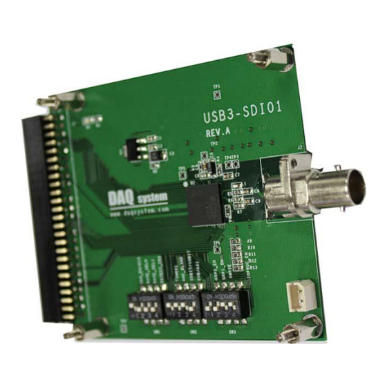
ADP-SDI01 User’s Manual(Rev(1.1) 2. ADP-SDI01 ADP-SDI01 is a simulator board that you can check or examine VANC data what’s going on to correct input and output to SDI port. Integration with USB3-DIO01, please refer to the manual. ADP-SDI01 Board USB3-SDI01 Rev. - Page 5 ADP-SDI01 User’s Manual(Rev(1.1) [Table 1. J1 Connector Descriptiopn] Name Description Remark +3.3V +3.3V Power +5V Power DIO_0 Digital Input/Output 0 Red Signal DIO_1 Digital Input/Output 1 Red Signal Digital Input/Output 2 Red Signal DIO_2 Digital Input/Output 3 Red Signal DIO_3 DIO_4 Digital Input/Output 4 Red Signal...
-
Page 6: J2 Connector
ADP-SDI01 User’s Manual(Rev(1.1) Digital Input/Output 30 DVAL DIO_30 Digital Input/Output 31 PCLK DIO_31 DIO_32 Digital Input/Output 32 To CA DIO_33 Digital Input/Output 33 DIO_34 Digital Input/Output 34 DIO_35 Digital Input/Output 35 DIO_36 Digital Input/Output 36 Digital Input/Output 37 DIO_37 DIO_38 Digital Input/Output 38 DIO_39 Digital Input/Output 39... -
Page 7: Sw1 Setting
ADP-SDI01 User’s Manual(Rev(1.1) 2.3 SW1 Setting 1 2 3 4 [Figure 2-4. SW1 switch] SDO_EN/DIS --- Control Signal Input/ Signal levels are LVCMOS / LVTTL compatible It is used to enable/disable the Serial Digital Output Stage. When SDO_EN/DIS is LOW, the serial digital output signals SDO and SDO are disabled and become high impedance. -
Page 8: Sw2 Setting
ADP-SDI01 User’s Manual(Rev(1.1) 2.4 SW2 Setting 1 2 3 4 [Figure 2-5. SW2 switch] TIM861 --- Control Signal Input/ Signal levels are LVCMOS / LVTTL compatible It is used to select the external CEA-861 timing mode. DETECT_TRS : 0, TIM861 : 0 the device extracts all internal timing from the supplied H:V:F(Hsync:VSync:Frame) timing signals. -
Page 9: Sw3 Setting
ADP-SDI01 User’s Manual(Rev(1.1) 2.5 SW3 Setting 1 2 3 4 [Figure 2-6. SW3 switch] GRP2..1EN --- Enables Audio Group 2..1 embedding. Set High to enable. SMPTE --- Control Signal Input/Signal levels are LVCMOS/LVTTL compatible It is used to enable/disable all forms of encoding/decoding, scrambling and EDH insertion. - Page 10 ADP-SDI01 User’s Manual(Rev(1.1) [Table 2. Register Setting] http://www.daqsystem.com...
Need help?
Do you have a question about the ADP-ADI01 and is the answer not in the manual?
Questions and answers