Table of Contents
Advertisement
Quick Links
Advertisement
Chapters
Table of Contents
Troubleshooting

Related Manuals for Nokia 616


Summary of Contents for Nokia 616
- Page 1 Nokia Customer Care SERVICE MANUAL Nokia 610 & 616 CarKit Phone (TFE-4/RV-1) (Approved Issue 1.0 November 2003) NMP Part No: 0275931 (Issue 1.1 December 2003) (Issue 2.0 March 2005) Company Confidential Copyright© 2005 Nokia Corporation, All Rights Reserved...
-
Page 2: Amendment Record Sheet
Inserted By Comments Number Issue 1.0 Nov. 03 P.Harvey Approved Issue Issue 1.1 Dec. 03 P.Harvey Published Issue Issue 2.0 Mar. 05 P.Harvey The introduction of the Nokia 616 Copyright © 2005 Nokia Corporation. Page 2 Issue 2.0 Mar/2005 Company Confidential... - Page 3 Under no circumstances shall Nokia be responsible for any loss of data or income or any special, incidental, consequential or indirect damages howsoever caused.
-
Page 4: Warnings And Cautions
4. Use only approved components as specified in the parts list. 5. Ensure all components, modules screws and insulators are correctly re- fitted after servicing and alignment. Ensure all cables and wires are repositioned correctly. Copyright © 2005 Nokia Corporation. Page 4 Issue 2.0 Mar/2005 Company Confidential... -
Page 5: For Your Safety
ESD protected spare part packages MUST NOT be opened/closed out of an ESD Protected Area. For more information and local requirements about ESD protec- tion and ESD Protected Area, contact your local Nokia After Mar- ket Services representative. Copyright © 2005 Nokia Corporation Issue 2.0 Mar/2005... -
Page 6: Care And Maintenance
All of the above suggestions apply equally to all the component parts of this product. Copyright © 2005 Nokia Corporation. Page 6 Issue 2.0 Mar/2005 Company Confidential... - Page 7 While every endeavour has been made to ensure the accuracy of this document, some errors may exist. If any errors are found by the reader, NOKIA MOBILE PHONES Busi- ness Group should be notified in writing.
- Page 8 Parts Lists & Component Layouts Service Software & Service Concepts Service Tools Disassembly & Assembly Instructions Troubleshooting Installation Technical Information Junction Board TF5 Engine Board TF4 Schematics and Component Finder Copyright © 2005 Nokia Corporation. Page 8 Issue 2.0 Mar/2005 Company Confidential...
-
Page 9: Nokia 610 & 616 Carkit Phone (Tfe-4/Rv
Nokia Customer Care Nokia 610 & 616 CarKit Phone (TFE-4/RV-1) 1 - General Information Copyright © 2005 Nokia Corporation. Issue 2.0 Mar/2005 Page 1-1 Company Confidential... -
Page 10: Table Of Contents
Table 4 : Supply voltages ....................... Table 5 : Power Consumption ....................... Table 6 : List of external connectors ................... Table 7 : Vibration conditions ....................... Table 8 : Temperature ranges ......................Copyright © 2005 Nokia Corporation. Page 1-2 Issue 2.0 Mar/2005 Company Confidential... -
Page 11: Abbreviations
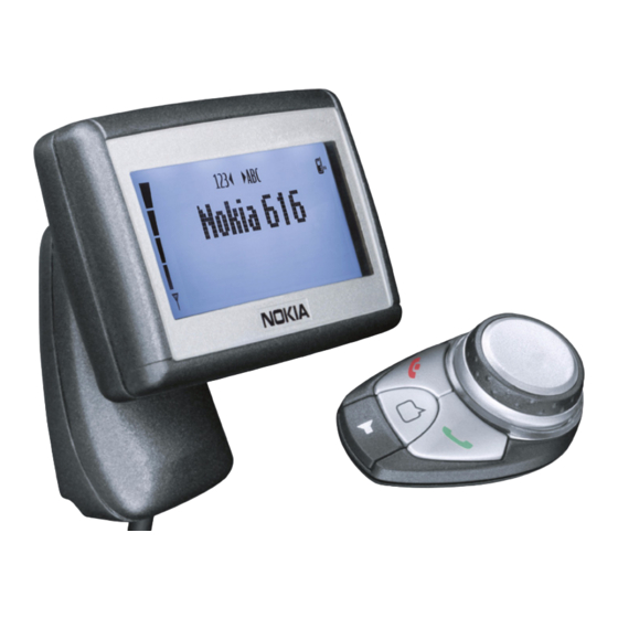
• As a fully functional car kit accessing a compatible mobile phone using Bluetooth Handsfree Profile. However, this offers a reduced feature set. Figure 1: Radio Unit TFE-4 Figure 1: Radio Unit TFE-4 Copyright © 2005 Nokia Corporation. Issue 2.0 Mar/2005 Page 1-3 Company Confidential... -
Page 12: Product Features
• Audio routing to headset (BT/headset) for privacy mode • Silent mode Voice recording • Record and playback voice memos/notes • Easy tracking and replay of up to 10 voice memos Copyright © 2005 Nokia Corporation. Page 1-4 Issue 2.0 Mar/2005 Company Confidential... -
Page 13: List Of Units And Modules
Table 1: Units and Modules Material code Notes Fig.1 Type Name of unit/module Item code 0051904 -------- Basic E&A incl. France, Czech, Slovak, Nokia 610 / 616 (TFE-4) SA and Poland. CarKit Phone Sales Pack 0051903 -------- Ukraine. 0051901 -------- Russia. 0051902... -
Page 14: Interconnection Diagrams
-106 dBm, EGSM900 TCH/FS at 2%BER -106 dBm, DCS1800 TCH/FS at 2%BER Frequency Error, Static Channel < 0.1 ppm RMS Phase Error < 5.0 Peak Phase Error < 20.0 Copyright © 2005 Nokia Corporation. Page 1-6 Issue 2.0 Mar/2005 Company Confidential... -
Page 15: Mechanical Characteristics
GSM antenna connector X101 IMS 3412.72.1610.001 Antenna connector FME RS232 Interface X102 Stewart SS-641010-NF-K1 Modular connector RJ-45 K1 Display Unit connector X103 Stewart SS-641010-A-NF-RMK4 Modular connector RJ-45 RMK4 Copyright © 2005 Nokia Corporation. Issue 2.0 Mar/2005 Page 1-7 Company Confidential... -
Page 16: Environmental Conditions
° ° Operation not guaranteed but an attempt to operate C to +80 will not damage the phone. Storage Non operational, 72 h ° ° C to +80 Copyright © 2005 Nokia Corporation. Page 1-8 Issue 2.0 Mar/2005 Company Confidential... - Page 17 Customer Care, User Guidance Nokia 610 & 616 CarKit Phone (TFE-4/RV-1) 2 - Parts List & Layouts Copyright © 2005 Nokia Corporation Issue 2.0 Mar/2005 Page 2-1 Company Confidential...
-
Page 18: Table Of Contents
Component layout diagram Bottom ............Component layout diagram Top ..............Parts List for TF5 Module (JB) ..................PWB component differences for N616 ............Component layout diagram for Bottom of TFE-5 ........Copyright © 2005 Nokia Corporation Page 2-2 Issue 2.0 Mar/2005 Company Confidential... -
Page 19: Exploded View Of Tfe-4 Radio Unit
Company Confidential TFE-4/RV-1 Nokia Customer Care 2 - Parts List Exploded view of TFE-4 Radio Unit Copyright © 2005 Nokia Corporation Issue 2.0 Mar/2005 Page 2-3 Company Confidential... -
Page 20: Assembly Parts List
50V normal,-5%,5% 0402C C122 Top Y 6 Chipcap 5% NP0 50V normal,-5%,5% 0402C C148 Top N CHIPCAP X5R 6.3V normal,-10%,10% 0603C C149 Top N CHIPCAP X5R 6.3V normal,-10%,10% 0603C Copyright © 2005 Nokia Corporation Page 2-4 Issue 2.0 Mar/2005 Company Confidential... - Page 21 CHIPCAP X5R 6.3V normal,-10%,10% 0603C C276 Top P CHIPCAP X5R 6.3V normal,-10%,10% 0603C C277 Top O CHIPCAP X5R 6.3V normal,-10%,10% 0603C C278 Top O CHIPCAP X5R 6.3V normal,-10%,10% 0603C Copyright © 2005 Nokia Corporation Issue 2.0 Mar/2005 Page 2-5 Company Confidential...
- Page 22 50V normal,-5%,5% 0402C C450 Top U Chipcap X7R 16V normal,-10%,10% 0402C C451 Top U CHIPCAP X5R 100n 10V normal,-10%,10% 0402C C454 Top S CHIPCAP X7R 100n 16V normal,-10%,10% 0603_BLM Copyright © 2005 Nokia Corporation Page 2-6 Issue 2.0 Mar/2005 Company Confidential...
- Page 23 50V normal,-10%,10% 0402C C721 Top H Chipcap X7R 50V normal,-10%,10% 0402C C722 Top H Chipcap 5% NP0 50V normal,-5%,5% 0402C C731 Top I Chipcap 5% NP0 50V normal,-5%,5% 0402C Copyright © 2005 Nokia Corporation Issue 2.0 Mar/2005 Page 2-7 Company Confidential...
- Page 24 L265 Top R FERRITE BEAD 0R5 600R/100MHz 0603_BLM L603 Top H CHIP COIL 3N9 +-0N3 Q28/800M 3n9H normal,-0n3,+0n3 0402L L604 Top H CHIP COIL 3N9 +-0N3 Q28/800M 3n9H normal,-0n3,+0n3 0402L Copyright © 2005 Nokia Corporation Page 2-8 Issue 2.0 Mar/2005 Company Confidential...
- Page 25 0402R R132 Top N Chipres 0W06 jumper normal,-,- 0402R R151 Top U RES NETWORK 0W06 2x1k0 normal,-5%,5% 0404_R_SR R152 Top U RES NETWORK 0W06 2x1k0 normal,-5%,5% 0404_R_SR Copyright © 2005 Nokia Corporation Issue 2.0 Mar/2005 Page 2-9 Company Confidential...
- Page 26 Resistor 5% 63mW normal,-5%,5% 0402R R610 Top M 5 Resistor 5% 63mW normal,-5%,5% 0402R R612 Top I Resistor 5% 63mW normal,-5%,5% 0402R R617 Top J Resistor 5% 63mW normal,-5%,5% 0402R Copyright © 2005 Nokia Corporation Page 2-10 Issue 2.0 Mar/2005 Company Confidential...
- Page 27 180R normal,-5%,5% 0402R T701 Top H TRANSF BALUN 1800+-100MHZ TRANS_LDB213 2X1.25 T702 Top K BALUN TRANS 3.7GHZ+/-300MHZ TRANS_LDB15 0805 V100 Top Y ZDIX4 TVS/ESD RSA6.1EN 6V1 SOT323_5L SOT353 Copyright © 2005 Nokia Corporation Issue 2.0 Mar/2005 Page 2-11 Company Confidential...
- Page 28 SAW FILT 942.5+-17.5MHZ/3.5 2.5X2 942.5MHz FILTER_SAW_SAFSD Z701 Top I SAW FILT 897.5+-17.5MHZ/3.5 2.5X2 897.5MHz FILTER_SAW_SAFSD Component layout diagram for the Bottom of the TF4 J102 J101 J103 J396 Copyright © 2005 Nokia Corporation Page 2-12 Issue 2.0 Mar/2005 Company Confidential...
- Page 29 Company Confidential TFE-4/RV-1 Nokia Customer Care 2 - Parts List Component layout diagram for the Top of the TF4 Copyright © 2005 Nokia Corporation Issue 2.0 Mar/2005 Page 2-13 Company Confidential...
-
Page 30: Parts List For Tf5 Module (Jb)
13 Chipcap 5% NP0 50V normal,-5%,5% 0402C C154 E 12 CHIPCAP X5R 1U M 50V 1210 50V normal,-20%,20% 1210C_H2.8 C155 13 CHIPCAP X5R 1U M 50V 1210 50V normal,-20%,20% 1210C_H2.8 Copyright © 2005 Nokia Corporation Page 2-14 Issue 2.0 Mar/2005 Company Confidential... - Page 31 C228 C 9 CHIPCAP NP0 1N0 J 50V normal,-5%,5% 0603C C229 D 6 CHIPCAP X5R 10U K 10V normal,-10%,10% 1206C_TDK C230 E 5 Chipcap 5% NP0 50V normal,-5%,5% 0402C Copyright © 2005 Nokia Corporation Issue 2.0 Mar/2005 Page 2-15 Company Confidential...
- Page 32 50V normal,-5%,5% 0402C C405 E 16 Chipcap 5% NP0 50V normal,-5%,5% 0402C C406 E 16 Chipcap X7R 10% 16V normal,-10%,10% 0402C C407 16 Chipcap 5% NP0 50V normal,-5%,5% 0402C Copyright © 2005 Nokia Corporation Page 2-16 Issue 2.0 Mar/2005 Company Confidential...
- Page 33 0603_VAR R103 C 12 CHIP VARISTOR VWM18V VC50V 0603_VAR R104 11 CHIPRES 0W06 2K87 F 200PPM 2k87 normal,-1%,1% 0402R R105 4 CHIPRES 0W06 1K0 F 200PPM normal,-1%,1% 0402R Copyright © 2005 Nokia Corporation Issue 2.0 Mar/2005 Page 2-17 Company Confidential...
- Page 34 R209 H 2 Chipres 0W06 6k8 F normal,-1%,1% 0402R R211 H 3 Chipres 0W06 22k F 200ppm normal,-1%,1% 0402R R212 H 3 Chipres 0W06 22k F 200ppm normal,-1%,1% 0402R Copyright © 2005 Nokia Corporation Page 2-18 Issue 2.0 Mar/2005 Company Confidential...
- Page 35 0402R R317 Q 6 Resistor 5% 63mW normal,-5%,5% 0402R R318 O 4 CHIPRES 0W06 1K0 F 200PPM normal,-1%,1% 0402R R319 M 5 Resistor 5% 63mW normal,-5%,5% 0402R Copyright © 2005 Nokia Corporation Issue 2.0 Mar/2005 Page 2-19 Company Confidential...
- Page 36 4 SCHDIX2 BAS70-07W 70V 70MA SOT343_R V301 5 SCHDIX2 BAS70-07W 70V 70MA SOT343_R V302 O 5 MFETX2 FDG6322C BIP.REPLAC SOT_363 V305 M 4 TRX2+RX4 UMH9N 50V 0.1A SOT_363 Copyright © 2005 Nokia Corporation Page 2-20 Issue 2.0 Mar/2005 Company Confidential...
-
Page 37: Pwb Component Differences For N616
7 EL. CAP. 20% 50V 100u 50V normal,-20%,20% Sanyo R304 M 7 CHIPRES 0W06 10K F normal,-5%,5% 0402R Deleted from N616 V113 Note: There are No components on bottom side of PWB. Copyright © 2005 Nokia Corporation Issue 2.0 Mar/2005 Page 2-21 Company Confidential... - Page 38 TFE-4/RV-1 Company Confidential 2 - Parts List Nokia Customer Care Component layout diagram for the Top of the TF5 Copyright © 2005 Nokia Corporation Page 2-22 Issue 2.0 Mar/2005 Company Confidential...
- Page 39 Nokia Customer Care Nokia 610 & 616 CarKit Phone (TFE-4/RV-1) 3 - Service Software Copyright © 2005 Nokia Corporation Issue 2.0 Mar/2005 Page 3-1 Company Confidential...
- Page 40 Delta Test description for AMS Service SW release ..........Self Test ......................... BB ADC Readings ......................Audio Testing ....................... Digital I/O Tests ......................SIM Test ......................... Engine module RF Alignment .................. Copyright © 2005 Nokia Corporation Page 3-2 Issue 2.0 Mar/2005 Company Confidential...
-
Page 41: Service Software
Phoenix is now ready to be used also with FPS-8 flash prommer and other tools. The Phoenix Service Software installation contains: • Service software support for all phone models included in the package Copyright © 2005 Nokia Corporation Issue 2.0 Mar/2005 Page 3-3 Company Confidential... -
Page 42: Phoenix Service Sw
Possible reasons may be defective or too old PKD-1Dongle (five digit serial number don- gle when used with FPS-8 Prommer) or that the FLS-4S POS Flash Dongle is defective or power to it is not supplied by external charger. Copyright © 2005 Nokia Corporation Page 3-4 Issue 2.0 Mar/2005... -
Page 43: Installing Phoenix
First, check the COM /parallel ports used! After correcting the problem, the installation can be restarted. Installing Phoenix Run the phoenix_service_sw_a12_2004_46_4_75.exe to start the installation. Install Shield will prepare. Click "Next" in Welcome dialog to continue. Copyright © 2005 Nokia Corporation Issue 2.0 Mar/2005 Page 3-5 Company Confidential... - Page 44 Choose the destination folder, it is recommended to use the default folder C:\Program- Files\Nokia\Phoenix. Choose “Next” to continue. You may choose another location by selecting “Browse” (not recommended). Setup copies the components, progress of the setup is shown. Please wait. Copyright © 2005 Nokia Corporation Page 3-6 Issue 2.0 Mar/2005 Company Confidential...
- Page 45 Drivers will be installed and updated, please wait. The process may take several minutes to complete. If the operating system does not require rebooting (Windows 2000, XP) the PC com- ponents are registered right away. Copyright © 2005 Nokia Corporation Issue 2.0 Mar/2005 Page 3-7 Company Confidential...
- Page 46 If the operating system used requires restarting your computer (Windows 98, SE, ME), the Install Shield Wizard will notify you about it. Select "Yes..." to reboot the PC immedi- ately and "No..." to reboot the PC manually afterwards. Copyright © 2005 Nokia Corporation Page 3-8 Issue 2.0 Mar/2005...
-
Page 47: Updating Phoenix Installation
To update Phoenix, you need to take exactly the same steps as when installing it for the first time. • Download the installation package to your computer hard disk. Copyright © 2005 Nokia Corporation Issue 2.0 Mar/2005 Page 3-9 Company Confidential... -
Page 48: Uninstalling Phoenix
Uninstallation can be done manually from Windows Control Panel - Add / Remove Pro- grams. Choose “Phoenix Service Software” and click "Add/Remove". Choose “Remove” to unin- stall Phoenix. Copyright © 2005 Nokia Corporation Page 3-10 Issue 2.0 Mar/2005 Company Confidential... - Page 49 TFE-4/RV-1 Nokia Customer Care 3 - Service Software Progress of the uninstallation is shown. If the operating system does not require rebooting, select “Finish” to complete. Copyright © 2005 Nokia Corporation Issue 2.0 Mar/2005 Page 3-11 Company Confidential...
-
Page 50: Repair
Phoenix. Note that the original installation package (e.g. phoenix_service_sw_a12_2004_46_4_75.exe) must be found on your PC when you run the repair setup. Copyright © 2005 Nokia Corporation Page 3-12 Issue 2.0 Mar/2005... - Page 51 "Add/Remove". In the following view choose “Repair”. Phoenix will reinstall components and register them, the procedure is the same as in the update installation. Choose “Finish” to complete. Copyright © 2005 Nokia Corporation Issue 2.0 Mar/2005 Page 3-13 Company Confidential...
-
Page 52: Data Package For Phoenix (Product Specific)
Installing Phoenix data package (product specific) Run the RV-1_dp_v_2.0_mucsw03.00.exe to start the installation. When you choose “Next” the files needed for the installation will be extracted. Please wait. Copyright © 2005 Nokia Corporation Page 3-14 Issue 2.0 Mar/2005 Company Confidential... - Page 53 There should be information about the Phoenix version needed with this data package. Choose “Next”. Confirm location and choose “Next” to continue. Install shield checks where the Phoenix application is installed and the directory is shown. Choose “Next” to continue. Copyright © 2005 Nokia Corporation Issue 2.0 Mar/2005 Page 3-15 Company Confidential...
- Page 54 TFE-4/RV-1 3 - Service Software Nokia Customer Care Choose “Next” to start copying the files. Phone model specific files will be installed. Please wait. Copyright © 2005 Nokia Corporation Page 3-16 Issue 2.0 Mar/2005 Company Confidential...
- Page 55 Now Phoenix can be used to for example flash phones and print type labels after: • configuring users • managing connections FLS-4S can be used right away. FPS-8* can be used after updating Flash Update Package files to it. Copyright © 2005 Nokia Corporation Issue 2.0 Mar/2005 Page 3-17 Company Confidential...
-
Page 56: Uninstalling The Data Package
Configuring Users Start Phoenix Service SW and Login. To add new user choose “Edit”. If user ID is already configured, choose your own user ID from the list and choose “OK”. Copyright © 2005 Nokia Corporation Page 3-18 Issue 2.0 Mar/2005... - Page 57 TFE-4/RV-1 Nokia Customer Care 3 - Service Software Choose “Add” to continue. Type in your name and initials to fields and choose “OK”. Copyright © 2005 Nokia Corporation Issue 2.0 Mar/2005 Page 3-19 Company Confidential...
-
Page 58: Managing Connections
Nokia Customer Care User has now been created, choose “OK”. You are now able to login with this username, choose “OK”. Managing Connections Start Phoenix Service SW and Login. Copyright © 2005 Nokia Corporation Page 3-20 Issue 2.0 Mar/2005 Company Confidential... - Page 59 To add new connection, choose “Add” and select if you want to create it manually or by using the Wizard. Choose “Next” to continue. In the next dialogs you will be asked to select some settings for the connection. Copyright © 2005 Nokia Corporation Issue 2.0 Mar/2005 Page 3-21 Company Confidential...
-
Page 60: Manual Settings
Activate the connection you want to use by clicking it and use up/down arrows to move it on top of the list. Choose “Apply”. The connection is now selected and can be used after closing the “Manage Connections” window. Copyright © 2005 Nokia Corporation Page 3-22 Issue 2.0 Mar/2005... -
Page 61: Updating Flash Support Files For Fps-8* And Fls-4
Updating Flash Support Files for FPS-8* and FLS-4* Before installation • Install Phoenix Service SW . Copyright © 2005 Nokia Corporation Issue 2.0 Mar/2005 Page 3-23 Company Confidential... -
Page 62: Installing The Flash Support Files (Only Separate Installation Package)
If you try to downgrade the existing version to older ones, the setup will be aborted. If you really want to downgrade, uninstall newer files manually from Control Panel and then re run the installation again. Copyright © 2005 Nokia Corporation Page 3-24 Issue 2.0 Mar/2005... - Page 63 It is highly recommended to install the files to the default destination folder C:\Program Files\Nokia\Phoenix. Choose “Next” to continue. When installing the flash update files for the first time you may choose another location by selecting “Browse” (not recom- mended).
- Page 64 The installation continues. Choose “Finish” to complete the procedure. FLS-4 can be used right after Flash Update Package is installed. FPS-8* flash prommer must be updated by using Phoenix! Copyright © 2005 Nokia Corporation Page 3-26 Issue 2.0 Mar/2005 Company Confidential...
-
Page 65: Updating The Fps-8* Flash Prommer Sw
Select ”Yes” to update files. The update procedure takes a couple of minutes, please wait until you are notified that update has been successful. Choose “OK” and close “FPS8 Maintenance” UI. Copyright © 2005 Nokia Corporation Issue 2.0 Mar/2005 Page 3-27... -
Page 66: Activating And Deactivating Fps-8
View after a successful prommer software update. FPS-8 sw can also be updated by pressing ”Update” and selecting appropriate fps8upd.ini file under C:\Program Files\Nokia\Phoenix\Flash. All files can be loaded separately to FPS-8. To do this, just press the right mouse button in the ”Flash box files”... -
Page 67: Activation
First, fill in the “FPS-8 activation request” sheet, in the FPS-8 sales package and follow the instructions in the sheet. When activation file is received (e.g. 00000.in), copy it to C:\ProgramFiles\Nokia\Phoe- nix\BoxActivation directory on your computer (this directory is created when Phoenix is installed). -
Page 68: Deactivation
Select “Deactivate” from the “FPS8 Maintenance” UI. Confirm Deactivation by choosing “Yes”. The box will be deactivated. Turn FPS-8 power off and on to complete deactivation. Copyright © 2005 Nokia Corporation Page 3-30 Issue 2.0 Mar/2005 Company Confidential... -
Page 69: Tfe-4/Rv-1 Delta Test Description
Refer to Delta test description for AMS Service SW release. Audio Testing Test description: Open the Audio Test Menu from the Testing drop down menu. Figure 1: Audio-Test setup Copyright © 2005 Nokia Corporation Issue 2.0 Mar/2005 Page 3-31 Company Confidential... -
Page 70: Digital I/O Tests
Open the Self Test Menu from the Testing drop down menu. Press the RUN Button to start the test. The test results will be displayed. Figure 2: Self-Test setup Copyright © 2005 Nokia Corporation Page 3-32 Issue 2.0 Mar/2005 Company Confidential... -
Page 71: Bb Adc Readings
Local Switch High Normal 44kR 49kR FLS-4S: 3K FLS-4S: 9K BTEMP 23°C 27°C VBAT 4,1V 4,4V Audio Testing Test description: STEP 1: Prepare Phoenix and Phone: -Activate Local Mode Copyright © 2005 Nokia Corporation Issue 2.0 Mar/2005 Page 3-33 Company Confidential... - Page 72 The Bias Voltage of the HF-MIC is to be measured with Voltmeter (<>5V). MIC-Path Frequency Generator Voltage Low Limit Upper Limit HDMIC 1000 30mV. 440mV (30dB) 705mV (40dB) HFMIC 1000 50mV 1280mV (15dB) 2050mV (20dB) Copyright © 2005 Nokia Corporation Page 3-34 Issue 2.0 Mar/2005 Company Confidential...
-
Page 73: Digital I/O Tests
SIM Test. Open the SIM Test Menu from the Testing drop down menu. Plug into SIM reader a functioning SIM card and press Update. (TF-4R Device has to be in Copyright © 2005 Nokia Corporation Issue 2.0 Mar/2005 Page 3-35... -
Page 74: Engine Module Rf Alignment
(against Tester). To check general Function a Call against Network (think of using a suitable Antenna) should be done. If the alignment is not as specified, the alignment can be done as with NHM-7. Copyright © 2005 Nokia Corporation Page 3-36 Issue 2.0 Mar/2005... -
Page 75: Service Tools
Nokia Customer Care Nokia 610 & 616 CarKit Phone (TFE-4/RV-1) 4 - Service Tools Copyright © 2005 Nokia Corporation Issue 2.0 Mar/2005 Company Confidential... - Page 76 Operating Mode ..................... SIM Reader ....................... Pin header ......................Service Test Connections ......................13 Module Jig concept ...................... 13 Final Test Setup-RCC (Call simulation with RC-Tester) ........14 Copyright © 2005 Nokia Corporation Page 4-2 Issue 2.0 Mar/2005 Company Confidential...
-
Page 77: List Of Service Tools
FPS-10 Flash Prommer • AC-33 Power Supply and cables • USB Cable CA-31D Note: The FPS-10 requires the following power cables: • JBV-1/DA-18 concept CA-41PS • FLA-41 concept CA-35S Copyright © 2005 Nokia Corporation Issue 2.0 Mar/2005 Page 4-3 Company Confidential... -
Page 78: Bt Testbox
Power cable for FPS-10 FLA-41 concept. PCS-1 Power Cable Connection between Power Supply and MJ-1. Connection between adjustable Power Supply and AD-2. CA-1S Flash Cable Connection between FLS-4S or FPS-8 to RU. Copyright © 2005 Nokia Corporation Page 4-4 Issue 2.0 Mar/2005 Company Confidential... -
Page 79: Serial Cable
Connection between FLS-4S or FPS-8 to MJ-1. CA-16UTS Audio Cable Service Cable, necessary for audio measurement. CA-29RS RF Cable Connection Cable between TFE-4/RV-1 RU and e.g. Radio Communication Tester. Copyright © 2005 Nokia Corporation Issue 2.0 Mar/2005 Page 4-5 Company Confidential... -
Page 80: Power Supply
Functionality ACW-4 Power Supply (13.gV, 3.6A) Power to AD-2. ACP-8E Power Supply (5.3V, 500mA) Power to JBT-9 ACF-8 Power Supply (6V, 2.1A) Power to FPS-8. Power to FLS-4S Copyright © 2005 Nokia Corporation Page 4-6 Issue 2.0 Mar/2005 Company Confidential... -
Page 81: Power Supply
IGNS signal can be switched on and off manually. During a call the CRM-line will be pulled down. This can be checked during GSM Go/ Nogo-Test. This will be indicated by a dedicated CRM-LED. Copyright © 2005 Nokia Corporation Issue 2.0 Mar/2005 Page 4-7... -
Page 82: Introduction
It is intended that the module jig should be used, under all circumstances, where an external supply to the phone is required while the phone is out of its mechanics. The supply voltage to the module jig is intended to be: 4.2V nominal. Copyright © 2005 Nokia Corporation Page 4-8 Issue 2.0 Mar/2005... -
Page 83: General Description Of The Test Pwb
Furthermore the Modul-Jig is equipped with guiding-needles to guide the engine PWB relative to the Test-PWB. The engine PWB testpatterns are connected to the Flash-/Audio connectors and to the pin header via needles Copyright © 2005 Nokia Corporation Issue 2.0 Mar/2005 Page 4-9 Company Confidential... -
Page 84: Connectors On Test Pwb
Flash Connector For the flash connector the standard pinning of the FPS-8 connector has been taken. For the TF4 the VPP, MBUS, FBUS_RX, FBUS_TX and BSI signals are used. Copyright © 2005 Nokia Corporation Page 4-10 Issue 2.0 Mar/2005 Company Confidential... - Page 85 Pin 1 is at the left side of the PWB connector (Face view). A K2 coded connector is used Switches on MJ-1 Power connector holder Testpoints Flash HFLOOP HDLOOP Copyright © 2005 Nokia Corporation Issue 2.0 Mar/2005 Page 4-11 Company Confidential...
-
Page 86: Operating Mode
1.8V level output of TF-4 1.8V supply of MJ-1 1.8V level output of TF-4 1.8V supply of MJ-1 PhonePWR Supply voltage for phone HF_Mute 1.8V level output of TF-4 Copyright © 2005 Nokia Corporation Page 4-12 Issue 2.0 Mar/2005 Company Confidential... -
Page 87: Service Test Connections
DC Power Cable 0730012 CA-16UTS Audio Test Cable 0730310 XRF-1 RF and AM Antenna Cable 0730085 DAU-9S Service Cable 0730108 PKD-1 SW Protection Key 0750018 ~~~~ Service SW ******** Copyright © 2005 Nokia Corporation Issue 2.0 Mar/2005 Page 4-13 Company Confidential... - Page 88 Final test setup-RCC (Call simulation with Radio Communication Tester) Item Type Description Part Code AD-2 Power Adapter 0770632 ACW-4 Power Supply for AD-2 0675227 CA-29RS RF Cable 0730320 Copyright © 2005 Nokia Corporation Page 4-14 Issue 2.0 Mar/2005 Company Confidential...
- Page 89 Customer Care Solutions Nokia 610 & 616 CarKit Phone (TFE-4/RV-1) 5 - Disassembly Instructions Copyright © 2005 Nokia Corporation. Issue 2.0 Mar/2005 Page 5-1 Company Confidential...
- Page 90 Remove Engine Unit ........................ Remove Frame ........................... Remove Data Cap ........................Remove the Junction Module ....................Assembly ............................Disassembly instructions for the SU-11/SU-21 ..............Disassembly instructions for the SIM flap ................. Copyright © 2005 Nokia Corporation. Page 5-2 Issue 2.0 Mar/2005 Company Confidential...
-
Page 91: Disassembly Instructions
1 to 9 with a torque load of 40 Ncm. Once assembled apply a new Warranty Seal label. 4. Bend the SIM Cover as shown and separate it from the Warranty Seal Label. Copyright © 2005 Nokia Corporation. Issue 2.0 Mar/2005 Page 5-3... - Page 92 7. Now remove the Engine Unit from the Frame. SIM reader is not soldered and can be removed easily. 8. Remove the Frame. Do not touch the spring contacts. Copyright © 2005 Nokia Corporation. Page 5-4 Issue 2.0 Mar/2005 Company Confidential...
-
Page 93: Remove Data Cap
Assembly after service will be carried out in the reverse order of the disassembly. Note: Before returning device to customer make sure to reseal with a new Warranty Seal label. All remains of the old one must be removed first. Copyright © 2005 Nokia Corporation. Issue 2.0 Mar/2005 Page 5-5... -
Page 94: Disassembly Instructions For The Su11/Su21
SIM Flap NOTE! For assembling Note: For assembly use the reverse order. reverse order use the reverse order A-Cover SIM Flap A-Cover SIM Flap Copyright © 2005 Nokia Corporation. LY INSTRUCTION SIM FLAP Issue 2.0 Mar/2005 Page 5-6 Company Confidential... -
Page 95: Disassembly Instructions For The Sim Flap
A-Cover SIM Flap NOTE! For assembling SIM Flap NOTE! For assembling 3. Carefully remove the SIM flap. use the reverse order Note: For assembly use the reverse order. Copyright © 2005 Nokia Corporation. Issue 2.0 Mar/2005 Page 5-7 Company Confidential... - Page 96 TFE-4/RV-1 Company Confidential 5 - Disassembly Instructions Nokia Customer Care This page has been intentionally left blank Copyright © 2005 Nokia Corporation. Page 5-8 Issue 2.0 Mar/2005 Company Confidential...
- Page 97 Customer Care Solutions Nokia 610 & 616 CarKit Phone (TFE-4/RV-1) 6 Troubleshooting & Final testing Copyright © 2005 Nokia Corporation Issue 2.0 Mar/2005 Page 6-1 Company Confidential...
- Page 98 Page No Introduction to TFE-4/RV-1 troubleshooting ............... General guidelines for TFE-4/RV-1 troubleshooting ............Tools needed for troubleshooting ................Low level troubleshooting for Nokia 610/N616 ..............Test-Setups for Troubleshooting ....................General Test Setup (Check Phone Information) ..............HW-setup ......................... Checking Phone Information/IMEI ................
- Page 99 Audio-Test setup ......................Extended Audio-Test setup ..................Audio-Test ........................Digital IO Test ......................... SIM Test set up ....................... SIM-Test .......................... SIM-Card inside TFE-4/RV-1 ..................Handsfree Call test set up ................... Copyright © 2005 Nokia Corporation Issue 2.0 Mar/2005 Page 6-3 Company Confidential...
- Page 100 TFE-4RV-1 Company Confidential Troubleshooting Nokia Customer Care This page has been intentionally left blank. Copyright © 2005 Nokia Corporation Page 6-4 Issue 2.0 Mar/2005 Company Confidential...
-
Page 101: Introduction To Tfe-4/Rv-1 Troubleshooting
• Service tools (as listed at service tools chapter in service manual) • Laboratory power supply with current indicator • Oscilloscope • Digital multimeter Low level troubleshooting for Nokia 610/N616 Fault symptom Source of fault and corrective action System doesn’t work at all DU doesn’t work/no DU illumination... -
Page 102: Test-Setups For Troubleshooting
Display-Connector of TFE-4/RV-1 (see figure 1) A power adapter AD-2 is necessary to supply 13.8V to the Radio Unit. (ACW-4 is the power supply for AD-2 power adapter) Copyright © 2005 Nokia Corporation Page 6-6 Issue 2.0 Mar/2005 Company Confidential... -
Page 103: Checking Phone Information/Imei
‘Phone Information’ from the drop down menue. The information will be read out automatically the first time, or can be forced to be read out by pressing the ‘Update’ button. Copyright © 2005 Nokia Corporation Issue 2.0 Mar/2005 Page 6-7... - Page 104 Basic production code Flash ID code Order number Production Number HW ID Those should be checked by reading out the Phone Information. Further the IMEI should be checked. Copyright © 2005 Nokia Corporation Page 6-8 Issue 2.0 Mar/2005 Company Confidential...
-
Page 105: Flashing On Pos Level
Service SW Installation Hints For the setup of the FLS-4S it is to be checked, which COM-Port is used for the FLS-4S. This can be checked in the control-panel within the Windows-Start-Menu/Settings. Copyright © 2005 Nokia Corporation Issue 2.0 Mar/2005 Page 6-9... -
Page 106: Scanning/Choosing Product
Otherwise, the phone cannot be scanned successfully. In this case a message will occur “No Product Found”. Scanning/Choosing Product If the Radio Unit is connected correctly and the Phoenix Service Software is started the Product shall be scanned. Copyright © 2005 Nokia Corporation Page 6-10 Issue 2.0 Mar/2005 Company Confidential... - Page 107 If this does not happen and the Message “No Product ” will be shown, the product can be manually selected under choose Product. Choose the Option TFE-4/RV-1 for the TFE-4/ RV-1 radio unit. Copyright © 2005 Nokia Corporation Issue 2.0 Mar/2005 Page 6-11...
- Page 108 Note, that probably still no software information will be indicated at the bottom line, but the selection for TFE-4/RV-1 is indicated. Additionally the Field for the Operating Mode will be empty. Copyright © 2005 Nokia Corporation Page 6-12 Issue 2.0 Mar/2005...
-
Page 109: Flashing
(TFE-4/RV-1) and the right product code are selected. The flash- files will be selected automatically, if not, they can also be changed by pressing the “set” button to browse for the needed ones. Copyright © 2005 Nokia Corporation Issue 2.0 Mar/2005 Page 6-13... -
Page 110: Flashing On Rcc Level
D9-D9 Cable incl. in FPS-8 sales pack 0730090 PKD-1 SW Protection Key 0750018 ~~~~ Service SW ******** Service SW Installation Hints Refer to previous section ’Flashing on POS Level’. Copyright © 2005 Nokia Corporation Page 6-14 Issue 2.0 Mar/2005 Company Confidential... -
Page 111: Selftest
Locals’ from the drop down menue. The test can be started by pushing the ‘Run Selftest’ button. All tests should be passed after the test has been done. Figure 6: Bluetooth Locals Copyright © 2005 Nokia Corporation Issue 2.0 Mar/2005 Page 6-15... -
Page 112: Bluetooth (Ber-)Test With Jbt-9
The JBT-9 Box can be used without any PC connection as loop-back device for BT test- ing. To verify the products BT functionality, a Bit Error Rate test needs to be performed against JBT-9. The test is controlled and executed by Phoenix service software. Copyright © 2005 Nokia Corporation Page 6-16 Issue 2.0 Mar/2005... -
Page 113: Attenuation Settings
TESTING INSTRUCTIONS FOR BER-TESTING • Make sure that the phone’s product support modules are properly loaded by Phoenix • Choose “Testing” and “Bluetooth Locals”. Copyright © 2005 Nokia Corporation Issue 2.0 Mar/2005 Page 6-17 Company Confidential... -
Page 114: Additional Menu Functions
• Other settings like “Scan Mode” or “BT Software Operational Mode” are only neces- sary to change in case of special device analysis in combination with e.g. commercial BT testsystems. Copyright © 2005 Nokia Corporation Page 6-18 Issue 2.0 Mar/2005... -
Page 115: Use Of Jbt-9 Bluetooth Fbus Interface
In Phoenix under the “File”, “Manage Connections” menu the Bluetooth connection has to be added. • Push down “Add” button and select the “Manual” mode. • Select “Bluetooth” as media: Copyright © 2005 Nokia Corporation Issue 2.0 Mar/2005 Page 6-19 Company Confidential... - Page 116 1 = PORT_NUM 1. • Give any name to the JBT-9 box. Default setting is “JBT-9”. If you have several boxes in range, separate names can be given to prevent any confusion. Copyright © 2005 Nokia Corporation Page 6-20 Issue 2.0 Mar/2005...
- Page 117 Default setting is MIN = minimum range. (0,1 – 0,5 m) • The JBT-9 box range for connection can be changed in the “BT_BOX_RANGE_INQUIRY” parameter setting. Default setting is MAX = maximum range (> 8 m). Copyright © 2005 Nokia Corporation Issue 2.0 Mar/2005 Page 6-21 Company Confidential...
-
Page 118: Establish A Bluetooth Fbus Conncetion To A Phone
COM1…” connection has been selected and is on the top. The green “BER TEST” LED on the JBT-9 box frontpanel will light up. The JBT-9 box starts an inquiary of all devices in range. First seen device will be asked for connection. Copyright © 2005 Nokia Corporation Page 6-22 Issue 2.0 Mar/2005... -
Page 119: Delete Pairing Devices Via Phoenix
During connection it is also possible to delete pairing devices and disconnect in one step. This can be done by with the functions “restore factory settings” or “restore service set- tings”. Copyright © 2005 Nokia Corporation Issue 2.0 Mar/2005 Page 6-23... -
Page 120: Attenuation Setting Via Jumper
• Start PHOENIX service software incl. installed PKD-1x dongle. • Make sure that in the actual selected connection is “NO CONNECTION”. • Select any phone with Bluetooth MCM in “Choose Product” menu. Copyright © 2005 Nokia Corporation Page 6-24 Issue 2.0 Mar/2005... - Page 121 • Open the “Bluetooth Flasher” as “Flashing” sub-menu. • Open the Select the correct “bin” file. Check the correct serial port (COM 1-4) port before. Press “Start” button and follow the pop-up menu. Copyright © 2005 Nokia Corporation Issue 2.0 Mar/2005 Page 6-25...
- Page 122 Nokia Customer Care • Wait until you get the “SUCCESS” response in the activity-window. The error mes- sage “MCM did not respond to Downloadmode On” can be ignored. Copyright © 2005 Nokia Corporation Page 6-26 Issue 2.0 Mar/2005 Company Confidential...
-
Page 123: Abbreviations
= Bit Error Rate = Bluetooth = Bluetooth F-Bus BTFB = (serial communication port) FBUS = (NOKIA proprietary communication bus) = Input / Output = Multi Chip Module = Personal Computer = Radio Frequency = (sub miniature RF connector type) -
Page 124: Audio Testing
Activate the loop to send the HF-Mic (hands free in) signal to the HF-Speaker (hands free out). When the HF-Mic is connected, blowing into the HF-Microphone shall be hearable in the HF-Speaker. Copyright © 2005 Nokia Corporation Page 6-28 Issue 2.0 Mar/2005... - Page 125 Power Adapter adjustable power supply ~13,5V Spea Signal Generator Remote Control CA-16UT Cable 1 Prepare Service Software 2 Activate Local Mode 3 Open Test menu / Audio Test Copyright © 2005 Nokia Corporation Issue 2.0 Mar/2005 Page 6-29 Company Confidential...
- Page 126 The Bias Voltage of the HF-MIC is to be measured with Voltmeter (<>5V). Generator Upper MIC-Path Frequency Voltage Limit Limit HDMIC 1000 30mV. 440mV (30dB) 705mV (40dB) HFMIC 1000 50mV 1280mV (15dB) 2050mV (20dB) Copyright © 2005 Nokia Corporation Page 6-30 Issue 2.0 Mar/2005 Company Confidential...
-
Page 127: Digital I/O Tests
• Deactivate “Display Power” option, Lights of the handset should be off now • Activate CRM option, LED at AD-2 Power adapter should lighten • Deactivate CRM light should be off now SIM-TEST Prepare the test set up as following: Copyright © 2005 Nokia Corporation Issue 2.0 Mar/2005 Page 6-31 Company Confidential... - Page 128 Plug a functioning SIM-Card into the SIM reader and press ‘Update’. (The TFE-4/RV-1 device has to be in the Test/Local mode). Figure 14: SIM-Test Figure 15: SIM-Card inside TFE-4/RV-1 Copyright © 2005 Nokia Corporation Page 6-32 Issue 2.0 Mar/2005 Company Confidential...
-
Page 129: Rf-Alignment
It should be noted that the supply voltage to the repair jig is intended to be nominal sup- ply voltage of 4.2V Copyright © 2005 Nokia Corporation Issue 2.0 Mar/2005 Page 6-33... -
Page 130: Call Test
Refer to Final test setup-RCC in chapter 4. PPCs Nokia 610 uses PPC’s, known from NPL-2. In addition three new PPC’s has been created especially for Nokia 610. The three new PPC’are: • SIM Insertion Counter •... - Page 131 Nokia Customer Care Nokia 610 & 616 Carkit Phone (TFE-4/RV-1) 7 - Installation Copyright © 2005 Nokia Corporation Issue 2.0 Mar/2005 Page 7-1 Company Confidential...
- Page 132 Power Cable PCU-4 ....................Technical data ....................Figures How to mount the RU in the car ................How to mount the Display Unit ................Power Cable PCU-4 ...................... Copyright © 2005 Nokia Corporation Page 7-2 Issue 2.0 Mar/2005 Company Confidential...
-
Page 133: Installation
• The CarKit Phone may only be installed by a qualified service technician using the approved original Nokia parts supplied in the sales package. Please note that non-observance of this requirement will result in loss of warranty. End users should remember that the car phone kit comprises complex technical equipment that requires professional installation using special tools and expert know-how. -
Page 134: Safety First
• In order to comply with RF exposure requirements for mobile transmitting devices, a minimum separation distance of 20 cm must be maintained between the antenna and all persons. Copyright © 2005 Nokia Corporation Page 7-4 Issue 2.0 Mar/2005 Company Confidential... - Page 135 Company Confidential TFE-4/RV-1 Nokia Customer Care 7 - Installation Nokia 610 CarKit Phone equipment Item Description Radio Unit TFE-4 Display Unit SU-11 Input Device CUW-3 Loudspeaker SP-2 Power Cable PCU-4 Handsfree Microphone HFM-8 GSM Antenna (not supplied) Copyright © 2005 Nokia Corporation Issue 2.0 Mar/2005...
-
Page 136: Mounting
TFE-4/RV-1 Company Confidential 7 - Installation Nokia Customer Care Nokia 616 CarKit Phone equipment Item Description Radio Unit RV-1 Display Unit SU-21 Input Device CUW-3 Loudspeaker SP-2 Handsfree Microphone HFM-8 Power Cable PCU-4 GSM Antenna (not supplied) Stickers Car Handset HSU-4 (not included) -
Page 137: Input Device Cuw-3
The Input device is supplied with a mount that is to be fixed in a suitable location where it is easily accessible to the user. As an alternative, the Nokia input device, type HSU-4 may be mounted for use with the CarKit Phone instead. However, take particular care to ensure that the input device will not interfere with the driver’s operation of the vehicle. -
Page 138: Microphone Hfm-8
• Direct connection to the supplied SP-2 loudspeaker. • Connection to a compatible car radio loudspeaker over an additional relay that switches audio output over to the loudspeaker. Copyright © 2005 Nokia Corporation Page 7-8 Issue 2.0 Mar/2005 Company Confidential... -
Page 139: Function Test
Current carrying capacity 1.5 A (standby mode 1 mA) Transmitting power EGSM 900 3.2 mW - 2 W DCS 1800 1.0 mW - 1 W Figure 3: Power Cable PCU-4 Copyright © 2005 Nokia Corporation Issue 2.0 Mar/2005 Page 7-9 Company Confidential... - Page 140 TFE-4/RV-1 Company Confidential 7 - Installation Nokia Customer Care This page has been deliberately left blank Copyright © 2005 Nokia Corporation Page 7-10 Issue 2.0 Mar/2005 Company Confidential...
- Page 141 Customer Care Solutions Nokia 610 & 616 CarKit Phone (TFE-4/RV-1) 8a - TF5 Technical Information Junction Board Copyright © 2005 Nokia Corporation. Issue 2.0 Mar/2005 Page 8a-1 Company Confidential...
- Page 142 Description of the HW Realization ............... Level shifter description ....................Block diagram of Levelshifter part ................ CRM Levelshifter ....................... Functional description ....................Antenna line ..........................Connectors ..........................B2B connectors ........................External connectors ......................Copyright © 2005 Nokia Corporation. Page 8a-2 Issue 2.0 Mar/2005 Company Confidential...
-
Page 143: Description
Figure 30: B2B power connectors ................Figure 31: B2B system connector ................. Figure 32: Input Device (ID) connector ................. Figure 33: Display unit connector ................Figure 34: Vcar connector .................... Copyright © 2005 Nokia Corporation. Issue 2.0 Mar/2005 Page 8a-3 Company Confidential... - Page 144 TFE-4/RV-1 Company Confidential TF5 Technical Information Nokia Customer Care This page has been intentionally left blank. Copyright © 2005 Nokia Corporation. Page 8a-4 Issue 2.0 Mar/2005 Company Confidential...
-
Page 145: Technical Information
TF5 Technical Information Technical Information TFE-4/RV-1, Nokia 610/616 are in-car GSM telephones which are permanently mounted in the vehicle and can be used to make and receive calls like any conventional hand-held GSM phone. The Radio Unit (RU) is powered by the car battery and some parts of the electronics are permanently powered for wakeup functionality. -
Page 146: Modes Of Operation
In GSM engine off mode, the GSM engine is switched off but the system remains pow- ered to keep an existing BT connection. The Local/Test mode is used for alignment and testing. Copyright © 2005 Nokia Corporation. Page 8a-6 Issue 2.0 Mar/2005... -
Page 147: Block Diagram
RS-232 is only used in N810 Electrical Module Description The Nokia 610/616 RU consist of two PWBs, one large board, designated TF5 and known as the JB, carries on it all the cable connector sockets and baseband electronics. It has six external cable connectors for connection of RF antenna, power, audio (2x) and user interface (2x). -
Page 148: Pwbs
• Drive-time optimized Car UI based on Jack3 monochrome • Optimized input device including wheel allowing blind usage during drive time • GPRS (General Packet Radio Service) • Bluetooth remote SIM access support for zero hassle usage (Nokia 610/616 only) • Support of BT headset • Handsfree capabilities •... -
Page 149: Blockdiagram Of Junctionboard
HS/ID B2BAUDIO Connector Mute HF-SPKR Vmic Connector VAudio VEBpwr Audio HF-MIC VEBPWR Connector Power connectors B2BCRM Dummy Levelshift Connector Antenna Line Figure 2: Block Diagram of the Junctionboard Copyright © 2005 Nokia Corporation. Issue 2.0 Mar/2005 Page 8a-9 Company Confidential... -
Page 150: Description Of The Powerstates
TFE-4/RV-1 Company Confidential TF5 Technical Information Nokia Customer Care Description of the Powerstates The Powerup/Powerdown-Behaviour for Nokia 610/616 is done as follows: Standby IGNITION POWERONX mode high Mode Carbattery valid Carbattery Carbattery fails fails Poweronx time elapsed Carbatt-Fail Mode Phoneengine... -
Page 151: Ignition Off Mode
System VSIM Baseb Connector VCORE VCar VWake VWAKE Regu- FLASH VFLASH1 lators VFLASH2 Power 4.2V SMPS Connector Blue >=1 Poweroffx tooth IGNS Supply TF-4 TF-5 Phone unit Junctionboard Copyright © 2005 Nokia Corporation. Issue 2.0 Mar/2005 Page 8a-11 Company Confidential... -
Page 152: Description Of The Blocks
B2BHFMUTE HF-Mode control signal High: 1.6..18V Here: VMIC will always be Low: 0..0.5V switched on (Sleepmode current too high) (when always high) Or always off (when always low) Copyright © 2005 Nokia Corporation. Page 8a-12 Issue 2.0 Mar/2005 Company Confidential... -
Page 153: Description Of The Hardware Realization
1mA standby demand. The Voltage VWAKE is used in the Power control block and as Backup-Battery replacement for the EB. When HF-Audiopath is activated, (B2BHFMute is high) the VWAKE power is directed to VMIC Copyright © 2005 Nokia Corporation. Issue 2.0 Mar/2005 Page 8a-13... - Page 154 VMIC is high, when one of both signals is high (OR logic). VWAKE Figure 6: VMIC switch (a) VMICONX driven low by B2BHFMUTEX Figure 7: VMIC switch (b) VMICONX driven low by B2BHDMUTEX Copyright © 2005 Nokia Corporation. Page 8a-14 Issue 2.0 Mar/2005 Company Confidential...
- Page 155 The power supply VAudio is used to supply the power amplifier for the HF speaker. It is designed by using low drop-regulator. Even when car voltage falls below 10V, it shall provide a slidely reduced Voltage level against Vcar on VAudio power line. Copyright © 2005 Nokia Corporation. Issue 2.0 Mar/2005 Page 8a-15...
- Page 156 Switch. Figure 10: VEBpwr regulator HW realization Copyright © 2005 Nokia Corporation. Page 8a-16 Issue 2.0 Mar/2005 Company Confidential...
-
Page 157: Power Control/Reset Block
Vcar, ignition-sense and the power control line B2BPoweroffx, provided by the EB. Further, it generates the Start-Up pulse on B2BPoweronx line to enable proper starting of the phone engine. Copyright © 2005 Nokia Corporation. Issue 2.0 Mar/2005 Page 8a-17... -
Page 158: Power Control/Reset Blockdiagram
SMPSon Low: 0..0.5V active (when always low) or after Ignition is switched off goes immediately low when ignition is switched off (when always high) Copyright © 2005 Nokia Corporation. Page 8a-18 Issue 2.0 Mar/2005 Company Confidential... - Page 159 Opendrain Output which 0V when Pow- Phoneunit will malfunction switches 47kR load to erok, else (SIM cannot be read), Phone Ground when Powerok is high impedance always in Localmode active Copyright © 2005 Nokia Corporation. Issue 2.0 Mar/2005 Page 8a-19 Company Confidential...
-
Page 160: Description Of The Hw Realization
Powerok will be forced to ground. This limit is determined by the combination R309/R310 and the 2.5V reference. SMPS startup IGNS5V Figure 14: SMPS startup realization Copyright © 2005 Nokia Corporation. Page 8a-20 Issue 2.0 Mar/2005 Company Confidential... - Page 161 The comparator N302 cares that the IGNS5V signal is only high when the Sense input is higher than 9V level. The 1.8V level shifter is realized by voltage divider R304/R307. Copyright © 2005 Nokia Corporation. Issue 2.0 Mar/2005 Page 8a-21...
-
Page 162: Description Of The Audio Block
HFMIC B2BHFMIC_n HFMIC HFAUDIO B2BXEAR_p HFSPKR B2BXEAR_n HFMute HFSPKR Levelshifter B2BHFMUTE B2BHDMIC_p B2BHDMIC_p B2BHDMIC_n B2BHDMIC_n HDMIC HDAUDIO HDEAR B2BHDMUTE HDMute HDSPKR Levelshifter Figure 18: Block Diagram of Audio-Block Copyright © 2005 Nokia Corporation. Page 8a-22 Issue 2.0 Mar/2005 Company Confidential... - Page 163 No Microphone Signal B2BHDMIC_N erated by Headset Micro- from Headset phone B2BHFMIC_P Symmetric Audio Signal gen- No Microphone Signal B2BHFMIC_N erated by Handsfree Micro- from Handsfree phone Amplifier Copyright © 2005 Nokia Corporation. Issue 2.0 Mar/2005 Page 8a-23 Company Confidential...
-
Page 164: Description Of The Hw Realization
Bias voltage is applied to the microphone. In the next stage the signal is multiplied by the amplifier N200. To set Bias level at the positive input of this amplifier the voltage 2Vbias is used. Copyright © 2005 Nokia Corporation. Page 8a-24 Issue 2.0 Mar/2005... - Page 165 With the HFMute signal coming from the HF-Mute Level-Shifter, the amplifier can be switched on (HSMUTE<1.5 V) or off (HSMUTE = >3.5V). VBIAS Regulator Figure 22: VBIAS Regulator Copyright © 2005 Nokia Corporation. Issue 2.0 Mar/2005 Page 8a-25 Company Confidential...
- Page 166 N200 and amplified to symmetric output signal within N202. The Amplifier can be muted by setting HDMUTE to high This signal comes from the HDMUTE level shifter. From B2BXEAR Figure 24: HD-Power amplifier realization Copyright © 2005 Nokia Corporation. Page 8a-26 Issue 2.0 Mar/2005 Company Confidential...
-
Page 167: Level Shifter Description
B2BXEAR lines when JB is standalone without phone engine. To HDSPKR and HFSPKR Figure 26: B2BXEAR Filter Level shifter Description Block Diagram of Levelshifter Part B2BCRM Figure 27: Block-Diagram of Level shifter Block Copyright © 2005 Nokia Corporation. Issue 2.0 Mar/2005 Page 8a-27 Company Confidential... -
Page 168: Crm Levelshifter
Depending on type of transistor, transistor will activate after some time again, but current will be limited to value of below 1.5A. Figure 28: CRM Realization Copyright © 2005 Nokia Corporation. Page 8a-28 Issue 2.0 Mar/2005... -
Page 169: Antenna Line
Company Confidential TFE-4/RV-1 Nokia Customer Care TF5 Technical Information Antenna Line Figure 29: Realization of the Antenna line Connectors B2B connectors Figure 30: B2B Power Connectors Copyright © 2005 Nokia Corporation. Issue 2.0 Mar/2005 Page 8a-29 Company Confidential... - Page 170 TFE-4/RV-1 Company Confidential TF5 Technical Information Nokia Customer Care Figure 31: B2B System-Connector Copyright © 2005 Nokia Corporation. Page 8a-30 Issue 2.0 Mar/2005 Company Confidential...
- Page 171 Company Confidential TFE-4/RV-1 Nokia Customer Care TF5 Technical Information External Connectors Figure 32: Input Device (ID) connector Figure 33: Display-Unit connector Copyright © 2005 Nokia Corporation. Issue 2.0 Mar/2005 Page 8a-31 Company Confidential...
- Page 172 TFE-4/RV-1 Company Confidential TF5 Technical Information Nokia Customer Care Figure 34: Vcar Connector Copyright © 2005 Nokia Corporation. Page 8a-32 Issue 2.0 Mar/2005 Company Confidential...
- Page 173 Customer Care Solutions Nokia 610 & 616 CarKit Phone (TFE-4/RV-1) 8a - TF5 Technical Information Junction Board Copyright © 2005 Nokia Corporation. Issue 2.0 Mar/2005 Page 8a-1 Company Confidential...
- Page 174 Description of the HW Realization ............... Level shifter description ....................Block diagram of Levelshifter part ................ CRM Levelshifter ....................... Functional description ....................Antenna line ..........................Connectors ..........................B2B connectors ........................External connectors ......................Copyright © 2005 Nokia Corporation. Page 8a-2 Issue 2.0 Mar/2005 Company Confidential...
- Page 175 Figure 30: B2B power connectors ................Figure 31: B2B system connector ................. Figure 32: Input Device (ID) connector ................. Figure 33: Display unit connector ................Figure 34: Vcar connector .................... Copyright © 2005 Nokia Corporation. Issue 2.0 Mar/2005 Page 8a-3 Company Confidential...
- Page 176 TFE-4/RV-1 Company Confidential TF5 Technical Information Nokia Customer Care This page has been intentionally left blank. Copyright © 2005 Nokia Corporation. Page 8a-4 Issue 2.0 Mar/2005 Company Confidential...
- Page 177 TF5 Technical Information Technical Information TFE-4/RV-1, Nokia 610/616 are in-car GSM telephones which are permanently mounted in the vehicle and can be used to make and receive calls like any conventional hand-held GSM phone. The Radio Unit (RU) is powered by the car battery and some parts of the electronics are permanently powered for wakeup functionality.
- Page 178 In GSM engine off mode, the GSM engine is switched off but the system remains pow- ered to keep an existing BT connection. The Local/Test mode is used for alignment and testing. Copyright © 2005 Nokia Corporation. Page 8a-6 Issue 2.0 Mar/2005...
- Page 179 RS-232 is only used in N810 Electrical Module Description The Nokia 610/616 RU consist of two PWBs, one large board, designated TF5 and known as the JB, carries on it all the cable connector sockets and baseband electronics. It has six external cable connectors for connection of RF antenna, power, audio (2x) and user interface (2x).
- Page 180 • Drive-time optimized Car UI based on Jack3 monochrome • Optimized input device including wheel allowing blind usage during drive time • GPRS (General Packet Radio Service) • Bluetooth remote SIM access support for zero hassle usage (Nokia 610/616 only) • Support of BT headset • Handsfree capabilities •...
-
Page 181: B2B Connectors
HS/ID B2BAUDIO Connector Mute HF-SPKR Vmic Connector VAudio VEBpwr Audio HF-MIC VEBPWR Connector Power connectors B2BCRM Dummy Levelshift Connector Antenna Line Figure 2: Block Diagram of the Junctionboard Copyright © 2005 Nokia Corporation. Issue 2.0 Mar/2005 Page 8a-9 Company Confidential... -
Page 182: Standbye Mode
TFE-4/RV-1 Company Confidential TF5 Technical Information Nokia Customer Care Description of the Powerstates The Powerup/Powerdown-Behaviour for Nokia 610/616 is done as follows: Standby IGNITION POWERONX mode high Mode Carbattery valid Carbattery Carbattery fails fails Poweronx time elapsed Carbatt-Fail Mode Phoneengine... - Page 183 System VSIM Baseb Connector VCORE VCar VWake VWAKE Regu- FLASH VFLASH1 lators VFLASH2 Power 4.2V SMPS Connector Blue >=1 Poweroffx tooth IGNS Supply TF-4 TF-5 Phone unit Junctionboard Copyright © 2005 Nokia Corporation. Issue 2.0 Mar/2005 Page 8a-11 Company Confidential...
-
Page 184: Description Of The Blocks
B2BHFMUTE HF-Mode control signal High: 1.6..18V Here: VMIC will always be Low: 0..0.5V switched on (Sleepmode current too high) (when always high) Or always off (when always low) Copyright © 2005 Nokia Corporation. Page 8a-12 Issue 2.0 Mar/2005 Company Confidential... -
Page 185: Description Of The Hardware Realization
1mA standby demand. The Voltage VWAKE is used in the Power control block and as Backup-Battery replacement for the EB. When HF-Audiopath is activated, (B2BHFMute is high) the VWAKE power is directed to VMIC Copyright © 2005 Nokia Corporation. Issue 2.0 Mar/2005 Page 8a-13... - Page 186 VMIC is high, when one of both signals is high (OR logic). VWAKE Figure 6: VMIC switch (a) VMICONX driven low by B2BHFMUTEX Figure 7: VMIC switch (b) VMICONX driven low by B2BHDMUTEX Copyright © 2005 Nokia Corporation. Page 8a-14 Issue 2.0 Mar/2005 Company Confidential...
- Page 187 The power supply VAudio is used to supply the power amplifier for the HF speaker. It is designed by using low drop-regulator. Even when car voltage falls below 10V, it shall provide a slidely reduced Voltage level against Vcar on VAudio power line. Copyright © 2005 Nokia Corporation. Issue 2.0 Mar/2005 Page 8a-15...
- Page 188 Switch. Figure 10: VEBpwr regulator HW realization Copyright © 2005 Nokia Corporation. Page 8a-16 Issue 2.0 Mar/2005 Company Confidential...
-
Page 189: Power Control/Reset Block
Vcar, ignition-sense and the power control line B2BPoweroffx, provided by the EB. Further, it generates the Start-Up pulse on B2BPoweronx line to enable proper starting of the phone engine. Copyright © 2005 Nokia Corporation. Issue 2.0 Mar/2005 Page 8a-17... -
Page 190: Power Control/Reset Blockdiagram
SMPSon Low: 0..0.5V active (when always low) or after Ignition is switched off goes immediately low when ignition is switched off (when always high) Copyright © 2005 Nokia Corporation. Page 8a-18 Issue 2.0 Mar/2005 Company Confidential... - Page 191 Opendrain Output which 0V when Pow- Phoneunit will malfunction switches 47kR load to erok, else (SIM cannot be read), Phone Ground when Powerok is high impedance always in Localmode active Copyright © 2005 Nokia Corporation. Issue 2.0 Mar/2005 Page 8a-19 Company Confidential...
-
Page 192: Description Of The Hw Realization
Powerok will be forced to ground. This limit is determined by the combination R309/R310 and the 2.5V reference. SMPS startup IGNS5V Figure 14: SMPS startup realization Copyright © 2005 Nokia Corporation. Page 8a-20 Issue 2.0 Mar/2005 Company Confidential... - Page 193 The comparator N302 cares that the IGNS5V signal is only high when the Sense input is higher than 9V level. The 1.8V level shifter is realized by voltage divider R304/R307. Copyright © 2005 Nokia Corporation. Issue 2.0 Mar/2005 Page 8a-21...
-
Page 194: Description Of The Audio Block
HFMIC B2BHFMIC_n HFMIC HFAUDIO B2BXEAR_p HFSPKR B2BXEAR_n HFMute HFSPKR Levelshifter B2BHFMUTE B2BHDMIC_p B2BHDMIC_p B2BHDMIC_n B2BHDMIC_n HDMIC HDAUDIO HDEAR B2BHDMUTE HDMute HDSPKR Levelshifter Figure 18: Block Diagram of Audio-Block Copyright © 2005 Nokia Corporation. Page 8a-22 Issue 2.0 Mar/2005 Company Confidential... - Page 195 No Microphone Signal B2BHDMIC_N erated by Headset Micro- from Headset phone B2BHFMIC_P Symmetric Audio Signal gen- No Microphone Signal B2BHFMIC_N erated by Handsfree Micro- from Handsfree phone Amplifier Copyright © 2005 Nokia Corporation. Issue 2.0 Mar/2005 Page 8a-23 Company Confidential...
-
Page 196: Description Of The Hw Realization
Bias voltage is applied to the microphone. In the next stage the signal is multiplied by the amplifier N200. To set Bias level at the positive input of this amplifier the voltage 2Vbias is used. Copyright © 2005 Nokia Corporation. Page 8a-24 Issue 2.0 Mar/2005... - Page 197 With the HFMute signal coming from the HF-Mute Level-Shifter, the amplifier can be switched on (HSMUTE<1.5 V) or off (HSMUTE = >3.5V). VBIAS Regulator Figure 22: VBIAS Regulator Copyright © 2005 Nokia Corporation. Issue 2.0 Mar/2005 Page 8a-25 Company Confidential...
- Page 198 N200 and amplified to symmetric output signal within N202. The Amplifier can be muted by setting HDMUTE to high This signal comes from the HDMUTE level shifter. From B2BXEAR Figure 24: HD-Power amplifier realization Copyright © 2005 Nokia Corporation. Page 8a-26 Issue 2.0 Mar/2005 Company Confidential...
-
Page 199: Level Shifter Description
B2BXEAR lines when JB is standalone without phone engine. To HDSPKR and HFSPKR Figure 26: B2BXEAR Filter Level shifter Description Block Diagram of Levelshifter Part B2BCRM Figure 27: Block-Diagram of Level shifter Block Copyright © 2005 Nokia Corporation. Issue 2.0 Mar/2005 Page 8a-27 Company Confidential... - Page 200 Depending on type of transistor, transistor will activate after some time again, but current will be limited to value of below 1.5A. Figure 28: CRM Realization Copyright © 2005 Nokia Corporation. Page 8a-28 Issue 2.0 Mar/2005...
- Page 201 Company Confidential TFE-4/RV-1 Nokia Customer Care TF5 Technical Information Antenna Line Figure 29: Realization of the Antenna line Connectors B2B connectors Figure 30: B2B Power Connectors Copyright © 2005 Nokia Corporation. Issue 2.0 Mar/2005 Page 8a-29 Company Confidential...
- Page 202 TFE-4/RV-1 Company Confidential TF5 Technical Information Nokia Customer Care Figure 31: B2B System-Connector Copyright © 2005 Nokia Corporation. Page 8a-30 Issue 2.0 Mar/2005 Company Confidential...
- Page 203 Company Confidential TFE-4/RV-1 Nokia Customer Care TF5 Technical Information External Connectors Figure 32: Input Device (ID) connector Figure 33: Display-Unit connector Copyright © 2005 Nokia Corporation. Issue 2.0 Mar/2005 Page 8a-31 Company Confidential...
- Page 204 TFE-4/RV-1 Company Confidential TF5 Technical Information Nokia Customer Care Figure 34: Vcar Connector Copyright © 2005 Nokia Corporation. Page 8a-32 Issue 2.0 Mar/2005 Company Confidential...
- Page 205 Customer Care Solutions Nokia 610 & 616 CarKit Phone (TFE-4/RV-1) 8b - TF4 Technical Information Engine Board Copyright © 2005 Nokia Corporation. Issue 2.0 Mar/2005 Page 8b-1 Company Confidential...
- Page 206 Audio ............................B2B-System connectors ...................... Block diagram ......................... HW Realization ....................... Description of BB self tests ....................ST_EAR_DATA_LOOP_TEST ..................ST_MBUS_RX_TX_LOOP_TEST ................... ST_SIM_CLK_LOOP_TEST ..................... ST_SIM_IO_CTRL_LOOP_TEST ..................ST_SLEEP_X_LOOP_TEST ..................... ST_TX_IDP_LOOP_TEST ....................Copyright © 2005 Nokia Corporation. Page 8b-2 Issue 2.0 Mar/2005 Company Confidential...
- Page 207 Figure 4: Baseband power distribution ..............Figure 5: UPP architecture ..................Figure 6: BT102 flash programming ................Figure 7: BT102 HW interface ..................Figure 8: UPP, UEM and SIM Connections ..............Copyright © 2005 Nokia Corporation. Issue 2.0 Mar/2005 Page 8b-3 Company Confidential...
- Page 208 TF4 Technical Information Nokia Customer Care Page Description Figure 9: Nokia 610/616 specific SIM realization ............Figure 10: Basic reading (Random access) ..............Figure 11: Write cycle to Flash ................... Figure 12: Truth table for PS=0 ................. Figure 13: Truth table for PS=1 .................
-
Page 209: Introduction
This document specifies the Baseband Module of the TF4 Engine Board of the TFE-4/RV- 1 (Nokia 610/616) program. The baseband module consists mainly the DCT-4 baseband engine chipset, and the B2B System and Power/RS232 Connector. The PWB is very similar to the NPL-1 Engine PWB. -
Page 210: Block Diagram Of Engine Board
UEM and distributed to the drivers. The UEM contains a real-time clock sliced down from the 32768 Hz crystal oscillator. The 32768 Hz clock is fed to the UPP as a sleep clock. Copyright © 2005 Nokia Corporation. Page 8b-6 Issue 2.0 Mar/2005... -
Page 211: Uem Startup/Powerdown Sequence
VBAT on the Engine Board) the UEM will be started by Poweron mode. During the Power-Up Sequence the UEM detects that the Poweronx line is pushed to ground by the Junction Board. Copyright © 2005 Nokia Corporation. Issue 2.0 Mar/2005 Page 8b-7... - Page 212 The symbol ' ' means that the voltage rises and ' ' that the voltage drops. '→' Means the result of the conditions set on the left most side. Copyright © 2005 Nokia Corporation. Page 8b-8 Issue 2.0 Mar/2005...
-
Page 213: Description Of The Uem-States
The UEM will recover from NO_SUPPLY into RESET mode if the VBAT voltage level rises above the V level by either reconnecting the main battery or charge it to such level. MSTR+ Copyright © 2005 Nokia Corporation. Issue 2.0 Mar/2005 Page 8b-9 Company Confidential... - Page 214 VANA is disabled and VR1 – VR7 are either disabled or in low quiescent mode. From SLEEP the UEM enters PWR_ON if SLEEPX goes high, PWR_OFF mode if watchdog elapses or BACK_UP mode if VBAT drops below V MSTR- Copyright © 2005 Nokia Corporation. Page 8b-10 Issue 2.0 Mar/2005 Company Confidential...
-
Page 215: Description Of The Powerstates
Active-Locked mode. In case that the ignition signal is going to low before that, a direct transition to the sleep mode will happen and the phone engine will be powered off immediately. Copyright © 2005 Nokia Corporation. Issue 2.0 Mar/2005 Page 8b-11... -
Page 216: Uem Power Supplies
SIM technologies. A register internally in the UEM controls the output of VSIM and can be written to by the MCU via the CBUS. The regulator VCORE is likewise adjust- Copyright © 2005 Nokia Corporation. Page 8b-12 Issue 2.0 Mar/2005... - Page 217 VR2-7 Boomer VSIM VCORE VANA Baseband Regulators FLASH VFLASH1 VFLASH2 VBAT Battery CHACON Backup battery DLR-3 switch Bluetooth IRDA PA Supply System Connecter Figure 4: Baseband power distribution Copyright © 2005 Nokia Corporation. Issue 2.0 Mar/2005 Page 8b-13 Company Confidential...
-
Page 218: Dc Characteristics
UEMSLX is slave to SleepX from the UPP. Sets the UEM into sleep mode. Condition in sleep-mode depends on MCU writings to UEM regulator registers solely. Condition in sleep-mode depends on DSP writings to UEM register. Copyright © 2005 Nokia Corporation. Page 8b-14 Issue 2.0 Mar/2005... -
Page 219: Upp
RAM for storing and manipulating SW variables. All the RAM-banks have a 145 MHz clock and 32-bit organization. It has also an ARM port interface, which is used for MCU/DSP message transfer (API). Copyright © 2005 Nokia Corporation. Issue 2.0 Mar/2005 Page 8b-15... -
Page 220: Bluetooth
The figure below illustrates the set-up used for BT102 flash programming. CBUS-Clk CBUS-Data CBUS-ENx BT102 LPRFINTREQ Level shift MBUS MBUS Men IF Main Flash FBUS-Tx FBUS-Tx Prommer FBUS-Rx FBUS-Rx Figure 6: BT102 flash programming Copyright © 2005 Nokia Corporation. Page 8b-16 Issue 2.0 Mar/2005 Company Confidential... -
Page 221: Bt-Hw Interface
BB reset PURX Logic "0" 0.20 Clock input SYSCLCK Signal 0.30 0.80 Vpp System clock amplitude input Frequency EN26MHZ Voltage 1.40 1.80 Defines system clock. "1" = 26 Copyright © 2005 Nokia Corporation. Issue 2.0 Mar/2005 Page 8b-17 Company Confidential... - Page 222 GPP0 LPRF Logic "1" 1.26 1.80 Sync Logic "0" 0.54 GPP1 LPRF Logic "1" 1.26 1.80 Logic "0" 0.54 GPP6 USART Logic "1" 1.26 1.80 Logic "0" 0.54 Copyright © 2005 Nokia Corporation. Page 8b-18 Issue 2.0 Mar/2005 Company Confidential...
- Page 223 BSI signal. The comparator offset is such that the comparator output does not alter state as long as the battery is connected. The BSI comparator threshold level is 2.1 V with 75 mV hysteresis. Copyright © 2005 Nokia Corporation. Issue 2.0 Mar/2005 Page 8b-19...
- Page 224 Supply voltage VSIM 3V SIM Card Icc, 4MHz Supply voltage 1.8V SIM Card Icc, 4MHz Ground 0.9*VSIM VSIM 0.15*VSIM SIM data DATA 0.7*VSIM VSIM Trise/Tfall max 1us 0.15*VSIM Copyright © 2005 Nokia Corporation. Page 8b-20 Issue 2.0 Mar/2005 Company Confidential...
-
Page 225: Sim
Company Confidential TFE-4/RV-1 Nokia Customer Care TF4 Technical Information Figure 9: Nokia 610/616 specific SIM Realization TF-4 TF-5R Connector Filter Vcar switch Connector Vflash1 Vflash1 Powermonitor R390 100k R202 Powerok 100k Within TFE-4/RV-1 there is a protection mechanism used to protect the Simcard when the car battery is out of range. -
Page 226: Slow Ad-Concept
Due to that the phone software can detect that the car battery is not in the right range. This is used to disable Simcard for protection purposes. Copyright © 2005 Nokia Corporation. Page 8b-22 Issue 2.0 Mar/2005... -
Page 227: Memory Description
The read cycle is initiated by first applying the address to the multiplexed address/data- bus. The address is latched at the rising edge of the AVD-signal. The memory device cap- Copyright © 2005 Nokia Corporation. Issue 2.0 Mar/2005 Page 8b-23... -
Page 228: Write Cycle
AVD or falling-edge of CE which ever occurs last. No clock is provided for a random access. The below figure shows a basic write waveform. Copyright © 2005 Nokia Corporation. Page 8b-24 Issue 2.0 Mar/2005... - Page 229 The status whether the data that is presented on the address/data bus is inverted or not, is indicated by a separate signal Copyright © 2005 Nokia Corporation. Issue 2.0 Mar/2005...
- Page 230 This means that the PS-signal is "0". The next scenario shows the opposite situation. Figure 13: Truth Table for PS=1 The comparison shows more unequal bits than equal bits, and the bits are inverted on the bus. Copyright © 2005 Nokia Corporation. Page 8b-26 Issue 2.0 Mar/2005 Company Confidential...
-
Page 231: Memory Block
A locked block can be unlocked by writing a "unlock block command" sequence, if the block is not locked-down. Copyright © 2005 Nokia Corporation. Issue 2.0 Mar/2005 Page 8b-27 Company Confidential... -
Page 232: Read While Write (Rww)
UPP wants to read from the flash. By using burst-mode the address only needs to be sent one time, then flash will keep sending data as long as there is a clock-signal. Figure 14: Description of Burst-Mode access Copyright © 2005 Nokia Corporation. Page 8b-28 Issue 2.0 Mar/2005... - Page 233 100mA Flash programming. Vcar 4.2VSMPS Car- Connector Igns >=1 Multiplexed To AD-2 /D t Flas Flashbus (FBUS RX/ FBUS TX/ MBUS) Connector BT-FBUS BT202 Powerok Btemp To FPS-8 Copyright © 2005 Nokia Corporation. Issue 2.0 Mar/2005 Page 8b-29 Company Confidential...
-
Page 234: Flash Concept On
"flash-programming mode" the UEM watchdog is disabled. When the bit is set it indicates "end of flash programming" and it resets the UEM watchdog timer to it’s default value. Clearing the flash programming bit also causes the UEM to generate a Copyright © 2005 Nokia Corporation. Page 8b-30 Issue 2.0 Mar/2005... -
Page 235: Mbus
UPP internal MCU SRAM. The MCU also ends up in "flash programming mode", if the contents of the flash is empty (reading FFH from the first memory location in the flash). Copyright © 2005 Nokia Corporation. Issue 2.0 Mar/2005 Page 8b-31... -
Page 236: Flash Identifiers
Codec, which will go over the Engine Audio Filter to the B2B connector. On the Junctionboard the Speaker amplifier is selected by the UPP-MCU pins HDMute or HFMute, which are also linked over the B2B connector. Copyright © 2005 Nokia Corporation. Page 8b-32 Issue 2.0 Mar/2005... - Page 237 HDMUTE TF5 Junction Board TF4 Phone Engine Figure 15: Block Diagram for TFE-1/RV-1 Audio Solution B2B System connector Figure 16: TFE-1/RV-1 specific realization of the Engine Audio filters Copyright © 2005 Nokia Corporation. Issue 2.0 Mar/2005 Page 8b-33 Company Confidential...
-
Page 238: B2B-System Connectors
VCAR 4.2V DC/DC IGNS conne ≥ 1 ctor B2BPoweroffx (Output 1.8V) B2BIgnition (Input 1.8V VIDD B2BCRM (output 1.8V) B2BUI_POWERON HS/ID conne B2BHSMUTEX ctor B2BHFMUTEX connector Audio TF-5R Spkr Copyright © 2005 Nokia Corporation. Page 8b-34 Issue 2.0 Mar/2005 Company Confidential... -
Page 239: Hw Realization
Company Confidential TFE-4/RV-1 Nokia Customer Care TF4 Technical Information HW Realization Figure 18: B2B System-Connector Copyright © 2005 Nokia Corporation. Issue 2.0 Mar/2005 Page 8b-35 Company Confidential... - Page 240 Figure 19: Realization of Control-IO Filter To B2B To UPP System connector Figure 20: Realization of Flash Filter To B2B To UEM System Connector Figure 21: VBACK Voltage divider Copyright © 2005 Nokia Corporation. Page 8b-36 Issue 2.0 Mar/2005 Company Confidential...
- Page 241 This function compares the ASIC version to the compilation flag. Major ASIC version in UPP version register is compared against ASIC version compilation flag. If the version is correct the result is ST_OK. If the version is wrong the result is ST_FAIL. Copyright © 2005 Nokia Corporation. Issue 2.0 Mar/2005 Page 8b-37...
- Page 242 Voltage provided by the Junctionboard and supported by System-B2B connector ST_SIM_LOCK_TEST This function shall test the SIM Lock. ST_LPRF_AUDIO_LINES_TEST Here the audio lines to the Bluetooth module shall be tested. Copyright © 2005 Nokia Corporation. Page 8b-38 Issue 2.0 Mar/2005 Company Confidential...
-
Page 243: Rf Troubleshooting
PWB. Capacitors can be checked for short-circuiting and resistors for value by means of an ohm-meter, but be aware in-circuit measurements should be evaluated carefully. In the following both, the name EGSM and EGSM900 will be used for the low Copyright © 2005 Nokia Corporation. Issue 2.0 Mar/2005 Page 8b-39... - Page 244 GSM1800/GSM1900 TX Balun V802 EGSM Pre-amplifier G701 3.7 GHz VCO T702 VCO Balun X602 RF (Board to Board) Connector L801 Directional Coupler V801 Detector Diode N801 Power Amplifier Copyright © 2005 Nokia Corporation. Page 8b-40 Issue 2.0 Mar/2005 Company Confidential...
-
Page 245: Rf Measurement Points
Figure 23: RF Supply points inside Mjoelner can VREF1 (C288) VR7 (C299) VR4 (C296) VR6 (C298) VR2 (C294) VR5 (C297) VR1A (C292) VR3 (C295) VIO (C218) Figure 24: RF Supply points inside and can Copyright © 2005 Nokia Corporation. Issue 2.0 Mar/2005 Page 8b-41 Company Confidential... - Page 246 There are no specific test points to measure RX I/Q signals. If necessary, RXIINN and RXQINN signals can be measured by removing the solder resist on top of the vias. Shown in the following picture. Copyright © 2005 Nokia Corporation. Page 8b-42 Issue 2.0 Mar/2005...
- Page 247 Pout EGSM CONT3 (VANTL) Figure 28: TX measurement points inside the PA can TXQOUTM TXQOUTP TXIOUTM TXIOUTP VTXB_900 TX_900 Figure 29: TX measurements points inside the Mjölner can Copyright © 2005 Nokia Corporation. Issue 2.0 Mar/2005 Page 8b-43 Company Confidential...
-
Page 248: Rf In General
The RF supports HSCSD (High Speed Circuit Switched Data) and GPRS (General Packed Radio Service), meaning multi-slot operation. This will not require special equipment or procedures in repair situations. Copyright © 2005 Nokia Corporation. Page 8b-44 Issue 2.0 Mar/2005 Company Confidential... - Page 249 PCS: 1850-1910 MHz RFCLK EGSM: 880-915 MHz I-signal Q-signal Figure 31: RF frequency plan On next page the RF block diagram is shown. Voltage supplies are marked with dotted lines. Copyright © 2005 Nokia Corporation. Issue 2.0 Mar/2005 Page 8b-45 Company Confidential...
- Page 250 TFE-4/RV-1 Company Confidential TF4 Technical Information Nokia Customer Care Figure 32: RF block diagram Copyright © 2005 Nokia Corporation. Page 8b-46 Issue 2.0 Mar/2005 Company Confidential...
-
Page 251: Rf Power Supply Configuration
13/26 MHz (SELADDR) 0.02 mA dig. interface (VDDDL) 1.35 V VREF01 bias reference (VBEXT) 100 uA 3.6 V VBAT Triple band PA, Bluetooth Figure 33: RF Power distribution diagram Copyright © 2005 Nokia Corporation. Issue 2.0 Mar/2005 Page 8b-47 Company Confidential... -
Page 252: Receiver
• The screen should now look like this: • Apply a signal with a frequency of EGSM : 942.467 MHz (channel 37 + 67.710kHz offset) GSM1800 : 1842.867 MHz (channel 700 + 67.710kHz offset) Copyright © 2005 Nokia Corporation. Page 8b-48 Issue 2.0 Mar/2005 Company Confidential... - Page 253 Step 2: Doing SNR Measurement • Select Maintenance /Testing/SNR Measurement • Select Fast SNR-Radio Button • The setup should now look like this: • Choose relevant band (EGSM900 / GSM1800) Copyright © 2005 Nokia Corporation. Issue 2.0 Mar/2005 Page 8b-49 Company Confidential...
- Page 254 Please refer to the fault finding chart for proper levels at different test points. Measuring analogue RX I/Q signal voltages using Oscilloscope Measuring with an oscilloscope on “RXIINN” or “RXQINN” is recommended only if RSSI Copyright © 2005 Nokia Corporation. Page 8b-50 Issue 2.0 Mar/2005...
- Page 255 37 or 700 or 661 Step 3: Doing the Measurement The following result should be seen with a working EGSM receiver: Signal amplitude 1.25V DC offset 1,35V Frequency 67kHz Copyright © 2005 Nokia Corporation. Issue 2.0 Mar/2005 Page 8b-51 Company Confidential...
-
Page 256: Fault Finding Chart For The Receiver
= to be done only once defective band only (common for all bands) Rx Signal paths The signal paths of the receiver are shown in following block diagram. Note that the pic- Copyright © 2005 Nokia Corporation. Page 8b-52 Issue 2.0 Mar/2005 Company Confidential... - Page 257 After amplification the RX signal is down-converted with a LO signal coming from the local oscillator. The RX paths of Mjoelner RF ASIC consist of following building blocks: • Separate LNAs for each of the two bands: EGSM900 and GSM1800. Copyright © 2005 Nokia Corporation. Issue 2.0 Mar/2005 Page 8b-53 Company Confidential...
-
Page 258: Egsm (Egsm900) Transmitter
• Select Maintenance/ Testing/ RF Controls. Wait until the RF Controls window pops up • Select: Band GSM 900 Active unit Operation mode Burst RX/TX Channel TX PA Mode Free TX Power Level TX Data Type Random Copyright © 2005 Nokia Corporation. Page 8b-54 Issue 2.0 Mar/2005 Company Confidential... -
Page 259: Tx Path Of The Transmitted Egsm900 Signal
VTXLOH Controls VTXBH VTXBL PCN/PCS OUTHP Balun OUTHM Open Dir. Coupler collector Open Buffer collector OUTLP OUTLM EGSM PLFB1 loop PLFB2 Mjølner filter VPCH/VPCL Supply filter PA_IDENT VBATTRF Copyright © 2005 Nokia Corporation. Issue 2.0 Mar/2005 Page 8b-55 Company Confidential... -
Page 260: Egsm900 Tx Path Of Mjoelner Rf Asic
Mjoelner RF ASIC using the control signals CONT1, CONT2 and CONT3. The following table shows the possible different states. CONT1 CONT2 CONT3 DCS/PCS EGSM Rx DCS Rx EGSM Tx [Volt] [Volt] [Volt] Copyright © 2005 Nokia Corporation. Page 8b-56 Issue 2.0 Mar/2005 Company Confidential... -
Page 261: Fault Finding Chart For Egsm900 Transmitter
Check Power Loop Pout_GSM) L801,V801 Power = +25 dBm, 897,4 MHz Check TXC Spectrum analyzer Check RF-connector Directional Coupler (L801) Pout =+23 dBm, 897,4 MHz Antenna Switch (Z601) EGSM TX Copyright © 2005 Nokia Corporation. Issue 2.0 Mar/2005 Page 8b-57 Company Confidential... -
Page 262: Gsm1800 (Dcs/Pcn) Transmitter
Now the measurement equipment should measure the following output signal from the phone. P = +20dBm @ 1747.8MHz If this is not the case, then go to the TX Troubleshooting section of this document for troubleshooting. Copyright © 2005 Nokia Corporation. Page 8b-58 Issue 2.0 Mar/2005 Company Confidential... -
Page 263: Fault Finding Chart For Gsm1800 Transmitter
Pout_DCS) L801,V801 Power = +22 dBm, 1747.8 MHz Check TXC Spectrum analyzer Check RF-connector Directional Coupler (L801) Pout = +20 dBm, 1747.8 MHz Antenna Switch (Z601) DCS TX Copyright © 2005 Nokia Corporation. Issue 2.0 Mar/2005 Page 8b-59 Company Confidential... -
Page 264: Tf-4 Synthesizer
= 3769.6MHz the tuning voltage should be 2.3V .. 2.8V (Tuning sensitivity of VCO is 240MHz/V typ.). If this is not the case, then go to section 1.4 of this document for troubleshooting. Copyright © 2005 Nokia Corporation. Page 8b-60 Issue 2.0 Mar/2005 Company Confidential... -
Page 265: 26 Mhz Reference Oscillator (Vcxo)
VR3;VIO and VREF01. This can be checked after power on for a time of PLL Block is functional Change VCO G701 about 32sec. After that time the voltages a going down.) Copyright © 2005 Nokia Corporation. Issue 2.0 Mar/2005 Page 8b-61 Company Confidential... - Page 266 It is important to note that the power supply of the VCXO (VR3) is only switched ‘OFF’ in the so-called ‘Deep Sleep Mode’ and power supply of VCO (G701 VR7) is switched ‘OFF’ in so-called ‘Sleep Mode’. Copyright © 2005 Nokia Corporation. Page 8b-62 Issue 2.0 Mar/2005...
- Page 267 Company Confidential TFE-4/RV-1 Nokia Customer Care TF4 Technical Information PLL Powersupply Loopfilter VCO and VCO power supply 26MHz Bluetooth buffer VR3 supply filter Copyright © 2005 Nokia Corporation. Issue 2.0 Mar/2005 Page 8b-63 Company Confidential...
- Page 268 914.2 959.2 3656.8 3836.8 902.0 947.0 3608.0 3788.0 914.4 959.4 3657.6 3837.6 902.2 947.2 3608.8 3788.8 914.6 959.6 3658.4 3838.2 902.4 947.4 3609.6 3789.6 914.8 959.8 3659.2 3839.2 Copyright © 2005 Nokia Corporation. Page 8b-64 Issue 2.0 Mar/2005 Company Confidential...
- Page 269 615 1730.8 1825.8 3461.6 3651.6 709 1749.6 1844.6 3499.2 3689.2 803 1768.4 1863.4 3536.8 3726.8 522 1712.2 1807.2 3424.4 3614.4 616 1731.0 1826.0 3462.0 3652.0 710 1749.8 1844.8 3499.6 3689.6 804 1768.6 1863.6 3537.2 3727.2 523 1712.4 1807.4 3424.8 3614.8 617 1731.2 1826.2 3462.4...
- Page 270 TFE-4/RV-1 Company Confidential TF4 Technical Information Nokia Customer Care This page has been deliberately left blank Copyright © 2005 Nokia Corporation. Page 8b-66 Issue 2.0 Mar/2005 Company Confidential...
- Page 271 Signal overview ................................Component finder TF4_05 ............................Car Radio mute, Display, Handset ..........................9-10 Power, Microphone ..............................9-11 Power ....................................9-12 RS232 connection ................................ 9-13 Component finder TF5_06 ............................9-14 Copyright © 2005 Nokia Corporation Issue 2.0 Mar/2005 Page 9-1...
-
Page 272: Schematics (Table Of Contents)
GENIO(52:0) SIMIF(3:0) Page 4 SIMIF(3:0) GENIO(52:0) Customer Care / Service & Support Readiness / Competence Transfer Team Copyright © 2005 NOKIA Only for training and service purposes Version: 2.0 18.01.2005 N610/N616 TFE-4/RV-1 Board version: TF5_06 DCT-4 common baseband Page 2(14) Copyright ©... -
Page 273: System Connector
Page 4 Customer Care / Service & Support Readiness / Competence Transfer Team & Support Readiness / Competence Transfer Team N610/N616 TFE-4/RV-1 Copyright © 2005 NOKIA Only for training and service purposes Version: 2.0 18.01.2005 Board version: TF5_06 System connector Page 3(14) Copyright ©... -
Page 274: Ueme, Sim
C291 GNDTH11 GNDTH15 GNDTH12 GNDTH16 Customer Care / Service & Support Readiness / Competence Transfer Team Copyright © 2005 NOKIA Only for training and service purposes Version: 2.0 Copyright © 2005 Nokia Corporation 18.01.2005 N610/N616 TFE-4/RV-1 Issue 2.0 Mar/2005 Board version: TF5_06... - Page 275 A3,C1,B10,D3= FLSRSTX J416 J417 J418 EXTWRX EXTRDX FLS2CSX J419 J420 FLSBAAX FLSPS FLSAVDX FLSCLK FLSCSX FLSRDY GENIO23 KEYB(10:0) GENIO24 Copyright © 2005 Nokia Corporation Issue 2.0 Mar/2005 Page 9-5 Customer Care / Service & Support Readiness / Competence Transfer Team...
- Page 276 Customer Care / Service & Support Readiness / Competence Transfer Team Copyright © 2005 Nokia Corporation Issue 2.0 Mar/2005 Page 9-6 N610/N616 TFE-4/RV-1 Copyright © 2005 NOKIA Only for training and service purposes Version: 2.0 18.01.2005 Board version: TF5_06 Bluetooth, Power connectors...
-
Page 277: Rf Part
Customer Care / Service & Support Readiness / Competence Transfer Team Copyright © 2005 Nokia Corporation Issue 2.0 Mar/2005 Page 9-7 N610/N616 TFE-4/RV-1 Copyright © 2005 NOKIA Only for training and service purposes Version: 2.0 18.01.2005 Board version: TF5_06 RF part... -
Page 278: Signal Overview
Copyright © 2005 Nokia Corporation Issue 2.0 Mar/2005 Page 9-8 Customer Care / Service & Support Readiness / Competence Transfer Team N610/N616 TFE-4/RV-1 Copyright © 2005 NOKIA Only for training and service purposes Version: 2.0 18.01.2005 Board version: TF5_06 Signal overview... -
Page 279: Component Finder Tf4_05
C280 P7 C703 B3 J404 S5 R104 X3 R710 L7 ustomer Care / Service & Support Readiness / Competence Transfer Team Copyright © 2005 Nokia Corporation Issue 2.0 Mar/2005 Page 9-9 opyright © 2005 NOKIA Only for training and service purposes Version: 2.0 18.01.2005 N610/N616 TFE-4/RV-1 Board version: TF5_06... -
Page 280: Car Radio Mute, Display, Handset
R420 VWM16V VWM16V C414 VWM16V Customer Care / Service & Support Readiness / Competence Transfer Team Copyright © 2005 NOKIA Only for training and service purposes Version: 2.0 18.01.2005 N610/N616 TFE-4/RV-1 Board version: TF5_06 Car Radio mute, Display, Handset Page 10(14) Copyright ©... -
Page 281: Power, Microphone
Page 10 R328 R328 E211 Customer Care / Service & Support Readiness / Competence Transfer Team N610/N616 TFE-4/RV-1 Copyright © 2005 NOKIA Only for training and service purposes Version: 2.0 18.01.2005 Board version: TF5_06 Power, Microphone Page 11(14) Copyright © 2005 Nokia Corporation Issue 2.0 Mar/2005... -
Page 282: Power
150k X103 BAS70-07W C146 V122 Page 10 BAS70-07W AUDIOV10 R114 V108 FLASHIMEI UM6K1N-TN C147 100n R139 C123 R115 100n AUDIOV10 V401 UM6K1N-TN V120 R142 UMH9N X110 V120 Page 10 B2BUIPOWERON Copyright © 2005 Nokia Corporation Issue 2.0 Mar/2005 Page 9-12... -
Page 283: Rs232 Connection
R505 RS232 "RTS" R506 RS232 Customer Care / Service & Support Readiness / Competence Transfer Team Copyright © 2005 NOKIA Only for training and service purposes Version: 2.0 18.01.2005 N610/N616 TFE-4/RV-1 Copyright © 2005 Nokia Corporation Board version: TF5_06 RS232 connection Page 13(14) Issue 2.0 Mar/2005... -
Page 284: Component Finder Tf5_06
R141 M15 R328 O4 Copyright © 2005 Nokia Corporation Issue 2.0 Mar/2005 Page 9-14 Customer Care / Service & Support Readiness / Competence Transfer Team Copyright © 2005 NOKIA Only for training and service purposes Version: 2.0 18.01.2005 N610/N616 TFE-4/RV-1 Board version: TF5_06...
Need help?
Do you have a question about the 616 and is the answer not in the manual?
Questions and answers