
Subscribe to Our Youtube Channel
Related Manuals for Arbor Technology EmETX-a5363


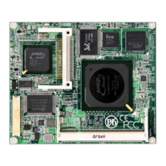
Summary of Contents for Arbor Technology EmETX-a5363
- Page 1 EmETX-a5363 ® AMD Geode™ ETX CPU Module User’s Manual Version 1.2 2010.11 Copyright® 2010 All Rights Reserved...
- Page 2 This page is intentionally left blank.
-
Page 3: Table Of Contents
Index Contents Chapter 1 - Introduction ..........1 1.1 Copyright Notice ..........2 1.2 About this User’s Manual ........2 1.3 Warning..............2 1.4 Replacing the lithium battery ......3 1.5 Technical Support ..........3 1.6 Warranty ............... 4 1.7 Packing List ............5 1.8 Ordering Information ........... - Page 4 Index 3.8 PNP/PCI Configurations ........36 3.9 PC Health Status ..........38 3.10 Load Optimized Defaults ........ 39 3.11 Set Password ..........40 3.12 Save to CMOS and Exit ........41 3.13 Exit Without Saving ......... 42 3.14 BIOS memory mapping ........43 3.15 Award BIOS Post Codes .........
-
Page 5: Chapter 1 Introduction
Introduction Chapter 1 Introduction Chapter 1 - Introduction - 1 -... -
Page 6: Copyright Notice
Introduction 1.1 Copyright Notice All Rights Reserved. The information in this document is subject to change without prior notice in order to improve the reliability, design and function. It does not represent a commitment on the part of the manufacturer. Under no circumstances will the manufacturer be liable for any direct, indirect, special, incidental, or consequential damages arising from the use or inability to use the product or documentation, even if advised of the possibility of such... -
Page 7: Replacing The Lithium Battery
Introduction 1.4 Replacing the lithium battery Incorrect replacement of the lithium battery may lead to a risk of explosion. The lithium battery must be replaced with an identical battery or a battery type recommended by the manufacturer. Do not throw lithium batteries into the trashcan. It must be disposed of in accordance with local regulations concerning special waste. -
Page 8: Warranty
Introduction 1.6 Warranty This product is warranted to be in good working order for a period of two years from the date of purchase. Should this product fail to be in good working order at any time during this period, we will, at our option, replace or repair it at no additional charge except as set forth in the following terms. -
Page 9: Packing List
Introduction 1.7 Packing List 1 x EmETX-a5363 AMD Geode™ ETX ® Module 1 x Driver CD 1 x Quick Installation Guide If any of the above items is damaged or missing, contact your vendor immediately. 1.8 Ordering Information EmETX-a5363VL/ AMD Geode™ LX800 ETX CPU module ®... -
Page 10: Specifications
Introduction 1.9 Specifications Form Factor AMD Geode™ ETX CPU Module ® Processor AMD Geode™ LX800@0.9W 500MHz Chipset AMD Geode™ CS5536 System Memory 1 x 200-pin SO-DIMM up to 1GB DDR SDRAM 2D Graphics Controller integrated in AMD Geode™ VGA Controller LX800 LCD: 24-bit TTL up to 1600 x 1200 (@60Hz) Display... -
Page 11: Board Dimensions
Introduction 1.10 Board Dimensions Top View 68.88 4- ø2.6 2.50 108.00 3.00 114.00 8.15 6.15 1.60 2.80 Unit: mm - 7 -... - Page 12 Introduction 2.50 108.00 3.00 Bottom View 114.00 8.15 6.15 1.60 2.80 Unit: mm 7.50 2.40 111.60 Unit: mm - 8 -...
-
Page 13: Chapter 2 Installation
Installation Chapter 2 Installation Chapter 2 - Installation - 9 -... -
Page 14: Block Diagram
Installation Block Diagram AMD Geode LX800 500MHz CPU Memory Bus 1 x 200-pin DDR SO-DIMM socket USB I/F Analog R.G.B. Geode CS5536 COM1 COM2 AC Link Audio AC’97 Super IO CODEC W83627HG LPT1/ FDD ALC203 LPC I/F IrDA, KB, MS PCI Bus 18-bit LVDS TTl to LVDS... -
Page 15: Connectors
Installation Connectors SODIMM1 - 11 -... -
Page 16: Lcd1: Ttl Lcd Connector
Installation LCD1: TTL LCD Connector Description Description VDD5 VDD5 VDD3 VDD3 N.C. LPD1 LPD0 LPD3 LPD2 LPD5 LPD4 LPD7 LPD6 LPD9 LPD8 LPD11 LPD10 LPD13 LPD12 LPD15 LPD14 LPD17 LPD16 LPD19 LPD18 LPD21 LPD20 LPD23 LPD22 FP_VS DOTCLK FP_HS ENVDD BLON CFD1: Compact Flash Tpe II Socket (Optional) Note:... -
Page 17: Etx1 Connector
Installation ETX1 Connector A1 GND GND A2 A3 PCICLK3 PCICLK4 A4 A5 GND GND A6 A7 PCICLK1 PCICLK2 A8 A9 REQ#3 GNT#3 A10 A11 GNT#2 VCC3 A12 A13 REQ#2 GNT#1 A14 A15 REQ#1 VCC3 A16 A17 GNT#0 N.C A18 A19 VCC VCC A20 A21 SERIRQ REQ#0 A22... -
Page 18: Etx2 Connector
Installation ETX2 Connector B1 GND GND B2 B3 SD14 SD15 B4 B5 SD13 MASTER# B6 B7 SD12 DREQ7 B8 B9 SD11 DACK#7 B10 B11 SD10 DREQ6 B12 B13 SD9 DACK#6 B14 B15 SD8 DREQ5 B16 B17 MEMW# DACK#5 B18 B19 MEMR# DREQ0 B20 B21 LA17 DACK#0 B22... -
Page 19: Etx3 Connector
Installation ETX3 Connector C1 GND GND C2 C3 R B C4 C5 HSY G C6 C7 VSY DDCK C8 C9 N.C DDDA C10 C11 N.C N.C C12 C13 N.C N.C C14 C15 GND GND C16 C17 N.C N.C C18 C19 N.C N.C C20 C21 GND GND C22... -
Page 20: Etx4 Connector
Installation ETX4 Connector D1 GND GND D2 D3 5V_SB PWGIN D4 D5 PS_ON SPEAKER D6 D7 PWERBTN# BATT D8 D9 N.C LILED D10 D11 RSMRST# ACTLED D12 D13 N.C SPEEDLED D14 D15 N.C I2CLK D16 D17 VCC VCC D18 D19 OVCR# N.C D20 D21 N.C I2DAT D22... -
Page 21: The Installation Paths Of Cd Driver
Installation The Installation Paths of CD Driver Driver Path CHIPSET \CHIPSET\AMD\LX \GRAPHICS\AMD\LX AUDIO \AUDIO\AMD\LX \Ethernet\REALTEK\8100C\9x.2K.XP - 17 -... - Page 22 Installation This page is intentionally left blank. - 18 -...
-
Page 23: Chapter 3 - Bios
BIOS Chapter 3 BIOS Chapter 3 - BIOS - 19 -... -
Page 24: Bios Introduction
BIOS 3.1 BIOS Introduction The Award BIOS (Basic Input/Output System) installed in your computer system’s. The BIOS provides for a standard device such as disk drives, serial ports and parallel ports. It also adds password protection as well as special support for detailed fine-tuning of the chipset controlling the entire system. -
Page 25: Standard Cmos Features
BIOS 3.3 Standard CMOS Features “Standard CMOS Features” allows you to record some basic hardware configurations in your computer system and set the system clock and error handling. If the CPU card is already installed in a working system, you will not need to select this option. - Page 26 BIOS IDE Primary HDDs The onboard PCI IDE connectors provide Primary channel for connecting up to two IDE hard disks or other IDE devices. Each channel can support up to two hard disks; the first is the “Master” and the second is the “Slave”. Press <Enter>...
- Page 27 BIOS Halt On This field determines whether or not the system will halt if an error is detected during power up. All errors (default) Whenever the BIOS detects a non-fatal error, the system will stop and you will be prompted. No errors The system boot will not be halted for any error that may be detected.
-
Page 28: Advance Bios Features
BIOS 3.4 Advance BIOS Features First/ Second Boot Device These fields determine the drive that the system searches first for an operating system. The options available include Setting: Floppy, HDD-0, SCSI, CDROM, HDD-1, USB-FDD, USB-ZIP, USB-CDROM, USB-HDD, LAN and Disabled. Boot Other Device It allows the system to search for an OS from other devices other than the ones selected in the First/ Second/ Third Boot Device. -
Page 29: Security Option
BIOS Security Option It allows you to limit access to the System and Setup. When you select System, the system prompts for the User Password every time you boot up. When you select Setup, the system always boots up and prompts for the Supervisor Password only when the Setup utility is called up. -
Page 30: Advanced Chipset Features
BIOS 3.5 Advanced Chipset Features CAS Latency It allows CAS latency time in HCLKs. The system board designer should set the values in this field, depending on the DRAM installed. Do not change the values in this field unless you change specifications of the installed DRAM or CPU. -
Page 31: Flat Panel Configuration
BIOS XOR MB0 Setting: Disabled (Default), Enabled. XOR Bit Select Setting: 18 (Default), 19, 20, 21. Video Memory Size In order to determine how much memory is allocated to the video graphics device. Setting: None, 8M (Default), 16M, 32M, 64M, 128M, 254M. Output display In order to specify the display devices the system is connected to. -
Page 32: Integrated Peripherals
BIOS 3.6 Integrated Peripherals On-Chip IDE Device >>> On-Chip IDE Channel 1 The integrated peripheral controller contains an IDE interface with support for two IDE channels. Select Enabled to activate each channel separately. Setting: Disabled, Enabled (Default). Master/Slave Drive PIO Mode It allows your system HDD controller to run faster. - Page 33 BIOS IDE Primary Master/Slave UDMA It allows your system to improve disk I/O throughput to 33MB/sec with the Ultra DMA33 feature. Setting: Disabled, Auto. IDE DMA Transfer Access Setting: Disabled, Enabled (Default). IDE HDD Block Mode It allows HDD controller to use the fast block mode to transfer data to and from HDD.
- Page 34 BIOS Onboard Serial/Parallel Port It allows you to select the onboard serial and parallel ports with their addresses. Setting: Serial Port 1 3F8/IRQ4 (Default) Serial Port 2 2F8/IRQ3 (Default) Parallel Port 378/IRQ7 (Default) UART Mode Select It determines the UART2 mode in your computer. Setting: IrDA, ASKIR, Normal (Default).
- Page 35 BIOS EPP Mode Select Setting: EPP1.9, EPP1.7 (Default) ECP Mode Use DMA Setting: 1, 3 (Default). IT8888 ISA Decode IO >>> It allows you to use the IT8888 ISA Decode IO menu to set the IO memory range for the onboard ISA. Decode I/O Space 0/ 1/ 2/ 3/ 4/ 5 It allows you to allocate system resources to the ISA bridge and to enable the function correctly.
- Page 36 BIOS Decode I/O Speed 0/ 1/ 2/ 3/ 4/ 5 It allows you to specify the speed of the ISA bus. Setting: Subtractive Speed, Slow Speed, Medium Speed, Fast Speed. Decode I/O Address 0/ 1/ 2/ 3/ 4/ 5 [15:4] It allows you to allocate an address to the ISA bus.
-
Page 37: Onboard Audio
BIOS Decode Memory Speed 0/ 1/ 2/ 3 It allows you to specify the memory speed of the ISA bus. Setting: Subtractive Speed, Slow Speed, Medium Speed, Fast Speed. Decode Memory Addr. 0/ 1/ 2/ 3 [23: It allows you to allocate a memory address to the ISA bus. The address may range from 0001 to 0FFF. -
Page 38: Power Management Setup
BIOS 3.7 Power Management Setup ACPI Function It supports ACPI (Advance Configuration and Power Interface). Setting: Enabled (Default), Disabled. Power Management It allows you to select the type of power saving management modes. Setting: APM Advanced power management (APM) ACPI (Default) Advanced Configuration and Power Interface (ACPI) Modem Use IRQ It sets the IRQ used by the Modem. - Page 39 BIOS Soft-Off by PWR-BTTN It defines the power-off mode when using an ATX power supply. In the Instant Off mode, It allows powering off immediately upon pressing the power button. In the Delay 4 Sec mode, the system powers off when the power button is pressed for more than 4 seconds or enters the suspend mode when pressed for less than 4 seconds.
-
Page 40: Pnp/Pci Configurations
BIOS 3.8 PNP/PCI Configurations PNP OS Installed It allows you to enable the PNP OS Install option if it is supported by the OS installed. Setting: No (Default), Yes. Reset Configuration Data It allows you to determine whether to reset the configuration data or not. Setting: Disabled (Default), Enabled. -
Page 41: Memory Resources
BIOS Memory Resources It allows you to configure the Memory Resources. PCI/VGA Palette Snoop Some non-standard VGA display cards may not show colors properly. It allows you to set whether or not MPEG ISA/VESA VGA cards can display with PCI/VGA. When “Enabled”, a PCI/VGA can display with an MPEG ISA/VESA VGA card. -
Page 42: Pc Health Status
BIOS 3.9 PC Health Status Current CPU Temperature CPU/ MEM VCore - 38 -... -
Page 43: Load Optimized Defaults
BIOS 3.10 Load Optimized Defaults It allows you to load the default values to your system configuration. The default setting is optimal and enabled all high performance features. - 39 -... -
Page 44: Set Password
BIOS 3.11 Set Password Using Password to set a password that will be used exclusively on the system. To specify a password, highlight the type you want and press <Enter>. The Enter Password: message prompts on the screen. Type the password, up to eight characters in length, and press <Enter>. -
Page 45: Save To Cmos And Exit
BIOS 3.12 Save to CMOS and Exit Typing “Y”, you will quit the setup utility and save all the changes into the CMOS memory. Typing “N”, you will return to Setup utility. - 41 -... -
Page 46: Exit Without Saving
BIOS 3.13 Exit Without Saving Typing “Y” will quit the Setup utility without saving the modifications. Typing “N” will return you to Setup utility. - 42 -... -
Page 47: Bios Memory Mapping
BIOS 3.14 BIOS memory mapping Address Device Description E000:0000h - F000:FFFFh System BIOS Area D000:2000h - D000:FFFFh Free space D000:0000h - D000:1FFFh LAN ROM C000:E000h - CF00:FFFFh Free space C000:0000h - C000:DFFFh VGA BIOS A000:0000h - B000:FFFFh VGA RAM 0000:0000h - 9000:FFFFh DOS 640K - 43 -... -
Page 48: Award Bios Post Codes
BIOS 3.15 Award BIOS Post Codes CFh Test CMOS read/write functionality C0h Early chipset initialization: Disable shadow RAM, L2 cache (socket 7 and below), program basic chipset registers Detect memory: Auto detection of DRAM size, type and ECC, auto detection of L2 cache (socket 7 and below) C3h Expand compressed BIOS code to DRAM C5h Call chipset hook to copy BIOS back to E000 &... - Page 49 BIOS Reserved HPM initialization (notebook platform) Reserved Check validity of RTC value; Load CMOS settings into BIOS stack. If CMOS checksum fails, use default value instead; Prepare BIOS resource map for PCI & PnP use. If ESCD is valid, take into consideration of the ESCD's legacy information;...
- Page 50 BIOS Initialize EISA slot Reserved Calculate total memory by testing the last double last word of each 64K page; Program writes allocation for AMD K5 CPU Reserved Reserved 4Ch Reserved 4Dh Reserved Program MTRR of M1 CPU; initialize L2 cache for P6 class CPU & program cacheable range;...
- Page 51 BIOS Reserved Reserved Reserved Enter AWDFLASH.EXE if: AWDFLASH.EXE is found in floppy drive and ALT+F2 is pressed Reserved Detect and install all IDE devices: HDD, LS120, ZIP, CDROM... Reserved Detect serial ports and parallel ports Reserved Reserved Detect and install coprocessor Reserved 7Ch Reserved 7Dh Reserved...
- Page 52 BIOS This page is intentionally left blank. - 48 -...
-
Page 53: Appendix
Appendix Appendix Appendix Appendix - 49 -... -
Page 54: Appendix-A I/O Port Address Map
Appendix Appendix-A I/O Port Address Map Each peripheral device in the system is assigned a set of I/O port addresses which also becomes the identity of the device. The following table lists the I/O port addresses used. Address Device Description EE000000 - EEFFFFFF Advanced Micro Devices Win 2K/XP Graphics Driver... - Page 55 Appendix 00000070 - 00000073 System CMOS/real time clock 00000170 - 00000177 Secondary IDE Channel 000001F0 - 000001F7 Primary IDE Channel 00000274 - 00000277 ISAPNP Read Data Port 00000279 - 00000279 ISAPNP Read Data Port 000002F8 - 000002FF Communications Port 00000376 - 00000376 Secondary IDE Channel 00000378 - 0000037F Printer Port...
-
Page 56: Appendix-B Interrupt Request Lines (Irq)
Appendix Appendix-B Interrupt Request Lines (IRQ) Peripheral devices use interrupt request lines to notify CPU for the service required. The following table shows the IRQ used by the devices on board. Level Function IRQ 01 Standard 101/102-Key or Microsoft Natural PS/2 Keyboard IRQ 03 Communications Port IRQ 04... -
Page 57: Appendix-C Watchdog Timer (Wdt) Setting
Appendix Appendix-C Watchdog Timer (WDT) Setting WDT is widely used for industry application to monitoring the activity of CPU. Application software depends on its requirement to trigger WDT with adequate timer setting. Before WDT time out, the functional normal system will reload the WDT. - Page 58 Appendix AX, 2Eh DX, AX AL, 0F0h DX, AL ; select CRF0 AL, 00h DX, AL ; set CRF0=00h, output AX, 2Eh DX, AX AL, 0F5h DX, AL ; select CRF5, WDT Timer unit AL, 00h ; bit2 =0 ->second ; bit2 =1 -> minute DX, AL ;...
- Page 59 Appendix C Language Code /*----- Include Header Area -----*/ #include "math.h" #include "stdio.h" #include "dos.h" /*----- routing, sub-routing -----*/ void main() outportb(0x2e, 0x87); /* initial IO port twice */ outp ortb(0x2e, 0x87); outportb(0x2e, 0x2B); /* select CR2B */ outportb(0x2e+1, 0x00); /* update CR2B bit4 to 00h */ /* Set PIN89 as WDTO */ outportb(0x2e, 0x07);...
- Page 60 Appendix This page is intentionally left blank. - 56 -...
Need help?
Do you have a question about the EmETX-a5363 and is the answer not in the manual?
Questions and answers