
Related Manuals for Advantech DSPC-8682


Summary of Contents for Advantech DSPC-8682
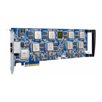
- Page 1 DSPC-8682 Octal-TMS320C6678 DSP PCI-E FLCard H/W Manual Author: Status: Version 1.0 Document ID: Location: Page...
-
Page 2: Table Of Contents
Content 1. GENERAL ......................6 .............................. 6 ENERAL NTRODUCTION ............................. 6 RODUCT PECIFICATIONS DSPC-8682 B ............................. 9 LOCK IAGRAMS DSPC-8682 PCI-E .......................... 10 CARD LACEMENT 2. HARDWARE SPECIFICATION ................11 ................................11 OWER ............................... 11 OWER ISTRIBUTION ............................... 14 OWER UDGET .............................. - Page 3 FIGURE 5: POWER DISTRIBUTION BLOCK DIAGRAM ............... 13 FIGURE 6: DSPC-8682 OVERALL POWER SEQUENCE ................ 15 FIGURE 7: POWER DISTRIBUTION ON DSPC-8682 PCI-E CARD ............16 FIGURE8: DSPC-8682 CARRIER CLOCK FEEDING DIAGRAM .............. 21 FIGURE9: DSPC-8682 RESET BLOCK DIAGRAM ................22 FIGURE10: THE DSP RESET SEQUENCE ON DSPC-8682 ..............
- Page 4 FIGURE31: THE SW1 SCHEMATIC ....................42 FIGURE32: THE SW2 SCHEMATIC ....................44 FIGURE33: DSPC-8682 TOP SIDE ..................... 46 FIGURE34: DSPC-8682 FRONT SIDE ....................46 FIGURE 35: DSPC-8682 BOTTOM SIDE .................... 47 Page...
- Page 5 Table TABLE 1: DSPC-8682 POWER BUDGET .................... 14 TABLE 2: SYSTEM POWER SEQUENCE PARAMETER ................. 16 TABLE 3: CLOCK DOMAINS ......................20 TABLE 4: PCI-E PORT MAPPING ON PEX8748 .................. 25 TABLE5: PCI-E SWITCH LED ......................30 TABLE6: FPGA LED ......................... 30 TABLE7: CN1 PIN ASSIGNMENT ......................
-
Page 6: General
General General Introduction This document is the H/W user manual of DSPC-8682, the PCI-E x8 Full-Length add-on card with octal-TMS320C6678 DSPs. DSPC-8682 is composed of eight TI TMS320C6678 DSPs, one PCI-E GEN3 switch PEX8748, one SRIO GEN2 switch CPS1616 and two RJ45 LAN ports. - Page 7 FPGA XILINX XC3S200AN Handle the DSPs’ interrupt events, booting configurations, power sequences, reset sequences and PHY LED control, programming clock generator of CDCE62005 and the LVDS clock buffers. PCI-express Switch PEX8748 (48 lanes / PCI-E GEN3) Upstream port: PCI-E x8 GEN3 to HOST, Downstream port: PCI-E GEN2x2 4-port to eight DSPs. Ethernet PHY BCM5482S Support 10/100/1000 Mb/s with 1000BASE-T interface.
- Page 8 PMBUS1: UCD9244 PMBUS connector. 560V2_PWR1: XDS560v2 power connector. Indicator Four LEDs, FPGA LED1 to FPGA LED4, are used for the FPGA XC3S200AN debugging. LED D1 indicates the error event of CPS1616. LED D3 indicates the error event of PEX8748. LED D4 indicates the interrupt event of PEX8748. LED SYSPG_D1 indicates that all power rails are stable.
-
Page 9: Dspc-8682 Block Diagrams
DSPC-8682 Block Diagrams The internal connections on DSPC-8682 PCI-E card are described and shown as below figures. The whole system interface block diagram for the DSPC-8682 board is shown as Figure 1 Each TMS320C6678 DSP contains several interfaces such as DDR, HyperLink, Serial RapidIO, PCI-E, and SGMII for Ethernet connection. -
Page 10: Dspc-8682 Pci-Ecard Placement
DSPC-8682 PCI-E card Placement Below figure shows main components on DSPC-8682. It’s only for reference if user needs to learn specific DSP or want to find a key chip on the card during developing. Figure 2: DSPC-8682 PCI-E card Placement... -
Page 11: Hardware Specification
Hardware Specification Power Feed The power source of DSPC-8682 is provided by two power rails, 12V and 3.3V from host, via PCI-E x8 golden finger and 12V from ATX power connector. Power Distribution The major power on DSPC-8682 is illustrated as below Figure3, Figure4 and Figure5. User could refer to DSPC-8682 schematics for more details regarding the power supplies on DSPC-8682. -
Page 12: Figure 4: Power Distribution Block Diagram For Dsp2, Dsp3, Dsp4 And Dsp5
TMS320C6678 TMS320C6678 DSP2 DSP4 DSP2_VartibleCore_1.0V DSP4_VartibleCore_1.0V VCC1P0 Adjus table Core Adjustable Core VCC1P0 1.0V/8A (0.9V – 1.1V) 10A (0.9V – 1.1V) 10A 1.0V/8A DVDD1P8 1.8V/0.416A DVDD1P8 1.8V/0.416A VCC1P5 VCC1P5 1.5V/1.3A 15A Max 15A Max 1.5V/1.3A VCC0P75 0.75V VCC0P75 0.75V UCD74110 UCD74110 DDR4 DDR4... -
Page 13: Figure 5: Power Distribution Block Diagram
3VSB@From PCIE MOSFET VCC3 3V@1.5A PG_VCC3 VCC12 MP28253EL VCC2P5 2.5V@1A Max. Delivery Current : 3A EN_VCC2P5 PG_VCC2P5 APL5912KAC VCC1P8_FPGA 1.8V@1A Max. Delivery Current : 1A 3VSB PG_VCC1P8_FPGA VCC1P2 MP28253EL 1.2V@1.1A Max. Delivery Current : 3A EN_VCC1V2 PG_VCC1P2 APL5912KAC VCC1P2SB 1.2VSB@0.2A Max. -
Page 14: Power Budget
Power Budget The estimated operational power budget of DSPC-8682 is about 152.06W. This value is estimated based on the assumption of the power dissipations and utilizations of the key components. For detailed number, it is summarized in the following table (Table1.DSPC-8682 Power Budget). -
Page 15: Power Sequence
Power Sequence DSPC-8682 consists of many devices on it, including DSP, PCIe switch, SRIO switch, PHY & FPGA etc. Hence, the power sequence is designed to meet all devices’ power-on requirements. And the timing parameters are shown in below table (Table 2.System Power Sequence Parameter) while the power sequence is shown in below figure.( Figure 6.DSPC-8682 overall power sequence). -
Page 16: Figure 7: Power Distribution On Dspc-8682 Pci-E Card
Table 2: System Power Sequence Parameter For the power sequence on each main component are designed based on the specifications of each chipset and shown in below figure (Figure7.Power distribution on DSPC-8682 PCIe card). FPGA XC3S200AN (VCCINT, VCCAUX, and VCCO supplies to the FPGA can be applied in any order) 1.2V/0.069A... -
Page 17: Platform Clock
Platform Clock The DSPC-8682 clocks are generated by the clock synthesizers, crystals and oscillators. Introductions for each clock are described as below. CDCE62005 : It’s a Low-Jitter clock generator with 25.0MHz crystal. It’s programmed to provide 166.66MHZ, 250MHZ and 100MHz with LVDS level for the DSP reference clocks. - Page 18 The platform clock distribution scheme is illustrated as the below Figure (Figure8.DSPC-8682 Carrier Clock Feeding Diagram). Signal Frequency Source Device DSP0_DDR_CLKP TI_CDCLVD110ARHBR 166.67MHz DSP0 DSP0_DDR_CLKN DSP1_DDR_CLKP TI_CDCLVD110ARHBR 166.67MHz DSP1 DSP1_DDR_CLKN DSP2_DDR_CLKP TI_CDCLVD110ARHBR 166.67MHz DSP2 DSP2_DDR_CLKN DSP3_DDR_CLKP TI_CDCLVD110ARHBR 166.67MHz DSP3 DSP3_DDR_CLKN...
- Page 19 Signal Frequency Source Device DSP3_SRIOSGMII_CLKP TI_CDCLVD110ARHBR 250.00MHz DSP3 DSP3_SRIOSGMII_CLKN DSP4_SRIOSGMII_CLKP TI_CDCLVD110ARHBR 250.00MHz DSP4 DSP4_SRIOSGMII_CLKN DSP5_SRIOSGMII_CLKP TI_CDCLVD110ARHBR 250.00MHz DSP5 DSP5_SRIOSGMII_CLKN DSP6_SRIOSGMII_CLKP TI_CDCLVD110ARHBR 250.00MHz DSP6 DSP6_SRIOSGMII_CLKN DSP7_SRIOSGMII_CLKP TI_CDCLVD110ARHBR 250.00MHz DSP7 DSP7_SRIOSGMII_CLKN DSP0_MCM_CLKP TI_CDCLVD110ARHBR 250.00MHz DSP0 DSP0_MCM_CLKN DSP1_MCM_CLKP TI_CDCLVD110ARHBR 250.00MHz DSP1 DSP1_MCM_CLKN DSP2_MCM_CLKP TI_CDCLVD110ARHBR 250.00MHz DSP2...
-
Page 20: Table 3: Clock Domains
Signal Frequency Source Device ICS583_PCIE_REF_CLKP7 IDT_ ICS853S12AKI 100.00MHz DSP7 ICS583_PCIE_REF_CLKN7 ICS583_PCIE_REF_CLKP8 IDT_ ICS853S12AKI PEX8748 100.00MHz ICS583_PCIE_REF_CLKN8 5482S_XTALO BCM5482SHA1KFBG 25.00MHz Crystal 5482S_XTALI XILINX XC3S200AN MAIN_48MHZ_CLK_R 48.00MHz Oscillator FPGA1 PCIE_REF_CLK_P PCI-E Gold Finger IDT_ICS853S12AKI 100MHz PCIE_REF_CLK_N 83PN156_XTAL_OUT ICS83PN156I 25.00MHz Crystal 83PN156_XTAL_IN 83PN156_SRIO_QN 80HCPS1616RMI 156.25MHz Oscillator... -
Page 21: Figure8: Dspc-8682 Carrier Clock Feeding Diagram
100Mhz Diff LVDS DSP0_PCIE_REF_CLKP/N DSP0_PCIE_REF_CLKP/N_LVDS DSP1_PCIE_REF_CLKP/N DSP1_PCIE_REF_CLKP/N_LVDS DSP2_PCIE_REF_CLKP/N DSP2_PCIE_REF_CLKP/N_LVDS DSP3_PCIE_REF_CLKP/N DSP3_PCIE_REF_CLKP/N_LVDS Divider resistor DSP4_PCIE_REF_CLKP/N DSP4_PCIE_REF_CLKP/N_LVDS PCIE_REF_CLK_P/N ICS853S12I DSP5_PCIE_REF_CLKP/N DSP5_PCIE_REF_CLKP/N_LVDS LVPECL DSP6_PCIE_REF_CLKP/N DSP6_PCIE_REF_CLKP/N_LVDS DSP7_PCIE_REF_CLKP/N DSP7_PCIE_REF_CLKP/N_LVDS PEX8748_REF_CLKP/N_LVDS PEX8748_REF_CLKP/N PEX8748 Transfer HCSL Figure8: DSPC-8682 Carrier Clock Feeding Diagram Page... -
Page 22: Reset Block Diagram
Reset Block Diagram DSPC-8682 reset mechanism is shown in Figure 9. DSPC-8682 Reset Block Diagram with below description of the reset sequence on DSPC-8682. The FPGA on the card will do the power-on sequence and make all power rails on the card be ready. -
Page 23: Reset Sequence
DSP power rails (CVDD, CVDD1, DVDD15 and DVDD18), reference clocks (core clock and DDR3 clock) and three reset events (RESETz, PORz and RESETFULLz). User can refer to TMS320C6678 Data Manual on TI webpage for the details. Figure10: The DSP Reset Sequence on DSPC-8682 Page... -
Page 24: Dsp (Ti Tms320C6678) Block Diagram
2.10 SRIO interface For SRIO connection, It’s has two kind of topology to link. The one DSPC-8682 adopts a ring topology to chain eight DSPs by one lane SRIO interface. One SRIO lane is connected to previous DSP while another lane is connected to next DSP on DSPC-8682, e.g. -
Page 25: Pci-Einterface
Figure12: Serial RapidIO Ring 2.11 PCI-E interface DSPC-8682 adopts a star topology to link host platform with two-lane PCIE interface via a PCI-E Gen3 switch, PEX8748. One PCI-E Gen2 port is designed with two Lanes (supports up to 5G baud per lane) connected to each DSP. -
Page 26: Ethernet Mac
BCM5482S by one lane SGMII interface. One SGMII lane is connected to previous DSP while another lane is connected to next DSP on DSPC-8682, e.g. the DSP#0 connects the DSP#1 with x1 SGMII port and connect the DSP#2 with another x1 SGMII port. -
Page 27: Hyperlink Interface
DSPC-8682 PCIE card. There are four-lane SerDes interface designed to operate up to 12.5Gbps per lane. The links of the HyperLink bus on DSPC-8682 are connected of the DSP#0 and the DSP#7as well as the DSP#1 and DSP#6, DSP#2 and DSP#5, DSP#3 and DSP#4) Below figure describes the Hyperlink connection on DSPC-8682. -
Page 28: Fgpa Xc3S200An
2.14 FGPA XC3S200AN For FPGA design, Xilinx XC3S200AN is implemented on DSPC-8682 for the power control, DSP boot configurations, programming clock generators and clock buffers and reset events for DPS farm. With the programmed FPGA on DSPC-8682, below functions are provided. -
Page 29: Figure16: Fpga Connection
XILINX_XC3S200AN VCC3 +V3.3 VCC2P5 HM_ALERT# PG_CVDD0_3 DVDD_1P8 PG_CVDD4_7 Hardware PG_VCC1P0_1 CLK_48M_HM W83795ADG Power VCC1P5 Montor PG_VCC1P0_2 PG_VCC1P5 VCC1P2 Sequences PG_DVDD1P8 SCL_HM Power Group PG_VCC2P5 VCC1P0 Control PG_VCC1P2 PG_VCC3 VCC0P9 VOLTERRA_VT237 x4 SDA_HM PG_VCC0P9 VCC5 PG_VCC5 MPS_MP28253EL x4 Temp_DSP0_3 EN_VCC3 UCD9244 x 2 EN_VCC2P5 Temp_DSP4_7 EN_DVDD1P8... -
Page 30: Leds
2.15 LEDs The locations of the LED indicators on the DSPC-8682 are shown by below figures. User can find the indicators easily for specific purpose. The detail descriptions are listed by following sections. Figure17: TOP Side LED Location There are two LEDs near PEX8748, the details are shown below (Table5) . - Page 31 established. The left side green LED present color when 100 BASE-TX Link is established. If left side LED is dark, it means 10 BASE-T link is established or no link is established. Page...
-
Page 32: Io Connector
IO Connector 3.1 Connector Overview This section describes the pin definition of the connectors on the DSPC-8682 PCIE card. User can have a detail on the pin signals for further use. For more details, please refer to the related documents from the website of the manufacturer. -
Page 33: The Pex8748, Bcm5482S And Cps1616 Boundary Scan Connector
3.2 The PEX8748, BCM5482S and CPS1616 boundary scan connector In this paragraph, we introduce the boundary scan connector for PEX8748, BCM5482S and CPS1616 CN1: The PEX8748, BCM5482S and CPS1616 boundary scan connector VCC3 R134 (106) CHAIN1_JTAG_TRSTN CHAIN1_JTAG_SW_CTRL (98) (103) CHAIN1_JTAG_TDI (98) CHAIN1_JTAG_TDO (106) -
Page 34: Tms320C6678 Boundary Scan Connector
3.3 TMS320C6678 Boundary Scan Connector In this paragraph, we introduce the boundary scan connector from the TMS320C6678 DSP. CN2: TMS320C6678 boundary scan connector VCC3 R126 (106) CONN40_TRSTN JTAG_SW_CTRL (18,106) (18) CONN40_TDO (106) CONN40_TDI (106) CONN40_TMS (106) CONN40_TCK PH_5x2V_S2.00mm 100pF 0402 Figure20: CN2, the Boundary Scan for the DSP farm Define Define... -
Page 35: Figure21: Cn3, Ti 60-Pin Emulation Connector
4.7K DSP0_EMU_18_R DSP0_EMU_18 R797 DSP_GP0_TRST# R842 CONN60_TRSTN_1.8V CONN60_TRSTN_1.8V (106) DSP0_EMU_16_R DSP0_EMU_16 R864 DSP0_EMU_15_R DSP0_EMU_15 R871 DSP0_EMU_13_R R872 DSP0_EMU_13 DSP0_EMU_11_R DSP0_EMU_11 R874 R120 NL/10K 1% DSP0_TCK_RR R875 DSP0_TCKRET DSP0_TCKRET (106) DSP0_EMU_10_R DSP0_EMU_10 R880 DSP0_EMU_08_R DSP0_EMU_08 R876 DSP0_EMU_06_R R885 DSP0_EMU_06 DSP0_EMU_04_R DSP0_EMU_04 R895 (87) TRGRSTZ... -
Page 36: Figure24: The Connection With Ti Xds560V2 Stm Emulator
Pin1 Figure24: The connection with TI XDS560v2 STM Emulator Col / Row EMU18 EMU17 TRST# EMU16 EMU14 EMU15 EMU12 EMU13 EMU11 Reserve TCLKRTN EMU9 EMU10 EMU7 EMU8 EMU5 EMU6 TCLK EMU4 EMU2 EMU3 EMU0 EMU1 TGRST# Table 9: CN3 DSP Emulator Pin Assignments Page... -
Page 37: Rj45 Lan Connector
3.5 RJ45 LAN connector In this paragraph, we introduce the RJ45 connector. CN4: RJ45 connector 5482S_LAN1_SPEED2 5482S_LAN1_SPEED2_R R167 (86) 5482S_LAN1_SPEED2 5482S_LAN1_SPEED1 R918 5482S_LAN1_SPEED1_R (86) 5482S_LAN1_SPEED1 5482S_RJ451_VCC 120_100MHz VCC2P5 0.5A TP0+ (95) 5482S_TRD1_0P 0.1uF TP0- (95) 5482S_TRD1_0N TP1+ (95) 5482S_TRD1_1P 0.1uF TP1- (95) 5482S_TRD1_1N... -
Page 38: Xilinx Xc3S200An Jtag Interface
LED1_ LINK LED2_ LINK LED1_ ACK LED2_ ACK LED1_SPEED2 B13 LED2_SPEED2 LED1_SPEED1 B14 LED2_SPEED1 Table10: CN4 Pin Assignment 3.6 XILINX XC3S200AN JTAG interface In this paragraph, we introduce the connector for Xilinx XC3S200AN JTAG interface. CN5: XILINX XC3S200AN JTAG interface 0.1uF 16V 3VSB FPGA_JTAG_TCK... -
Page 39: Dc 12V Atx Power Connector
3.7 DC 12V ATX power connector In this paragraph, we introduce the 4-pin 12V ATX connector used to support 12V current rating for DSPC-8682. VCC12_ATX C2531 C663 C661 10uF 10uF 0.1uF ATX_3x2H_4.2mm <Characteristic> Figure27: CN6, 12V connector Define Table12: CN6 Pin Assignment... -
Page 40: Fan Connector
3.8 FAN connector In this paragraph, we introduce the FAN connector. CN7: FAN connector FAN CNN1 30_100MHz C2569 C668 10uF 0.1uF WB_3V_2.0mm R1488 4.7K BAS32L 300mA R1472 FAN_SPEED1 R1446 Figure28: CN7, FAN connector Define Fan speed Table13: CN7 Pin Assignment Page... -
Page 41: Fan Connector
3.9 FAN connector In this paragraph, we introduce the FAN connector. CN8: FAN connector FAN CNN2 B108 30_100MHz C2574 C2571 10uF 0.1uF WB_3V_2.0mm R679 4.7K BAS32L 300mA R1464 FAN_SPEED2 R1463 Figure29: CN8, FAN connector Define Fan speed Table14: CN8 Pin Assignment Page... -
Page 42: Jumper And Switch Setting
DSP farm by the FPGA. Below figure shows the position of the 4-bit sliding switch. Figure30: The SW1 on DSPC-8682 PCIe Card Below figure shows the sliding switch circuit and notes the bit number for use. VCC3V3_FPGA... -
Page 43: Table15: The Sw1 Setting Table
This mode is booting DSP from PCIE interface. SW1.bit[4:2] : others- reserved for future use. The default setting of the switch (SW1) on DSPC-8682 is 0x0011b (bit[4:1]: ON, ON, OFF, OFF) for little endian data format and EEPROM boot from 0x51h. -
Page 44: Figure32: The Sw2 Schematic
4.2 S-RIO port wide switch There is one 4-bit sliding switch (SW2) on the board to set the SRIO configuration. The default routing table was flashed on EEPROM is SRIO 2x. (It need to re-flash EEPROM if need to change the setting from 2x to 1x.) Below figure shows the position of the 4-bit sliding switch. -
Page 45: Table16: The Sw2 Setting Table
The settings of Jumper and switch for DSPC-8682 are described as below table. Configuration Bit4 Bit3 Bit2 Bit1 Description QCF[1], QCF[3], The SRIO ports of CPS1616 QCF[5], QCF[7] configure to 2x. (default) (0000) The SRIO ports of CPS1616 QCF[1], QCF[3], configure to 1x. -
Page 46: Mechanical Drawing
Mechanical Drawing Figure33: DSPC-8682 TOP side Figure34: DSPC-8682 Front Side Page... -
Page 47: Figure 35: Dspc-8682 Bottom Side
Figure 35: DSPC-8682 Bottom Side Page...
Need help?
Do you have a question about the DSPC-8682 and is the answer not in the manual?
Questions and answers