Sign In
Upload
Download
Table of Contents
Contents
Add to my manuals
Delete from my manuals
Share
URL of this page:
HTML Link:
Bookmark this page
Add
Manual will be automatically added to "My Manuals"
Print this page
×
Bookmark added
×
Added to my manuals
Manuals
Brands
Clevo Manuals
Laptop
P650SE
Service manual
Clevo P650SE Service Manual
Hide thumbs
1
2
3
4
5
6
7
8
9
10
Table Of Contents
11
12
13
14
15
16
17
18
19
20
21
22
23
24
25
26
27
28
29
30
31
32
33
34
35
36
37
38
39
40
41
42
43
44
45
46
47
48
49
50
51
52
53
54
55
56
57
58
59
60
61
62
63
64
65
66
67
68
69
70
71
72
73
74
75
76
77
78
79
80
81
82
83
84
85
86
87
88
89
90
91
92
93
94
95
96
97
98
99
100
101
102
103
104
105
106
107
108
109
110
111
112
113
114
115
116
117
118
119
120
121
122
123
124
125
126
page
of
126
Go
/
126
Contents
Table of Contents
Bookmarks
Table of Contents
Instructions for Care and Operation
Power Safety
Battery Precautions
System Startup
Table of Contents
Introduction
Overview
Specifications
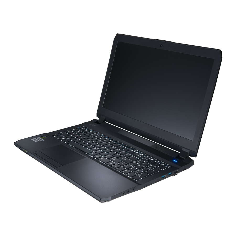
External Locator - Top View with LCD Panel Open
External Locator - Front & Right Side Views
External Locator - Left Side & Rear View
External Locator - Bottom View
Mainboard Overview - Top (Key Parts)
Mainboard Overview - Bottom (Key Parts)
Mainboard Overview - Top (Connectors)
Mainboard Overview - Bottom (Connectors)
Disassembly
Overview
Maintenance Tools
Connections
Maintenance Precautions
Disassembly Steps
Removing the Keyboard
Removing the Battery
Removing the Hard Disk Drive
Removing the System Memory (RAM)
Removing the M.2 SSD Module
Removing the Wireless LAN Module
Wireless LAN, Combo, 3G & LTE Module Cables
Removing and Installing the 3G/SATA Module
Part Lists
Part List Illustration Location
Bottom
Main Board
Hdd
Lcd
Schematic Diagrams
Processor 1/7-DMI, FDI, PEG
Processor 2/7- CLK, MISC
Processor 3/7- (DDR3L
Processor 4/7- Display
Processor 5/7- Power
Processor 6/7- POGND
Processor 7/7- RSVD
Ddr3 Cha So-Dimm_0
Ddr3 Cha So-Dimm_1
Ddr3 Chb So-Dimm_0
Ddr3 Chb So-Dimm_1
Panel, Inverter
Rtd2136N-Cg
Mini DP Port D
Mini DP Port B
HDMI Connector
VGA PCI Express
VGA Frame Buffer Partition
Frame Buffer Partition a
Frame Buffer Partition B
Frame Buffer Partition A_B
GPU Frame Buffer Partition
Frame Buffer Partition C
Frame Buffer Partition D
Frame Buffer Partition C_D
GPU Decoupling
DACA Interface XTAL
IFP I/O Interface
Misc - GPIO, I2C and ROM
GPU NVVDD, FBVDDQ, and GND
Lynx 1/9
Lynx 2/9
Lynx 3/9
Lynx 4/9
Lynx 5/9
Lynx 6/9
Lynx 7/9
Lynx 8/9
Lynx 9/9
USB3.0 + Esata Combo
USB Charger
M.2 3G + M.2 Sata
Wlan+Bt, Pcie4X Ssd
Realtek ALC892
Tpa2008D2
Subwoofer
Kbc-Ite It8587
Tpm, CCD, Tp
Fan, LID, KB, LED, G Sensor
Connector
Ddr 1.35V / 0.75Vs, Pch 1.5V
Vdd3, Vdd5
5V, 5Vs, 3.3V, 3.3Vs, 3.3Va
1.05 Series
Ac_In, Charger
POWER V-Core1
Pex_Vdd, 3V3_Aon, 3V3_Run
NVVDD Phase 1 & 2
Fbvddq
Audio Board
Power Board
HDD Board
LED Board
Finger Sensor Board
Click Board
USB Board 1/4
USB Board 2/4
USB Board 3/4
USB Board 4/4
USB Board 4/4
Power Board
LED Board
Updating the FLASH ROM BIOS
Download the BIOS
Unzip the Downloaded Files to a Bootable CD/DVD or USB Flash Drive
Set the Computer to Boot from the External Drive
Use the Flash Tools to Update the BIOS
Restart the Computer (Booting from the HDD
Advertisement
Quick Links
1
Specifications
2
Mainboard Overview - Top (Key Parts)
3
Removing the Keyboard
4
Removing the M.2 Ssd Module
5
Use Flash Tools to Update BIOS
Download this manual
P650SE / P651SE
Table of
Contents
Previous
Page
Next
Page
1
2
3
4
5
Advertisement
Table of Contents
Need help?
Do you have a question about the P650SE and is the answer not in the manual?
Ask a question
Questions and answers
Related Manuals for Clevo P650SE
Laptop Clevo P651SE Service Manual
(126 pages)
Laptop Clevo P650RA Service Manual
(132 pages)
Laptop Clevo P650HS Service Manual
(148 pages)
Laptop Clevo P650HP6 Service Manual
(134 pages)
Laptop Clevo P650SA Service Manual
(126 pages)
Laptop Clevo P650SG Service Manual
(126 pages)
Laptop Clevo P651SG Service Manual
(126 pages)
Laptop Clevo P670SG Service Manual
(130 pages)
Laptop Clevo P640RF Series Service Manual
(25 pages)
Laptop Clevo P640RF Service Manual
(112 pages)
Laptop Clevo P6x0Hx User Manual
(368 pages)
Laptop Clevo P670SE Service Manual
(130 pages)
Laptop Clevo P670RG Series Service Manual
(134 pages)
Laptop Clevo P671RG Service Manual
(134 pages)
Laptop Clevo P670SA Service Manual
(126 pages)
Laptop Clevo P670RE Service Manual
(134 pages)
This manual is also suitable for:
P651se
Table of Contents
Save PDF
Print
Rename the bookmark
Delete bookmark?
Delete from my manuals?
Login
Sign In
OR
Sign in with Facebook
Sign in with Google
Upload manual
Upload from disk
Upload from URL


Need help?
Do you have a question about the P650SE and is the answer not in the manual?
Questions and answers