Table of Contents
Advertisement
SERVICE MANUAL
Ver 1.0 1999.03
NTSC MODEL : DCR-TRV410/TRV510
PAL MODEL
: DCR-TRV410E/TRV510E
MICROFILM
DCR-TRV410/TRV410E/
TRV510/TRV510E
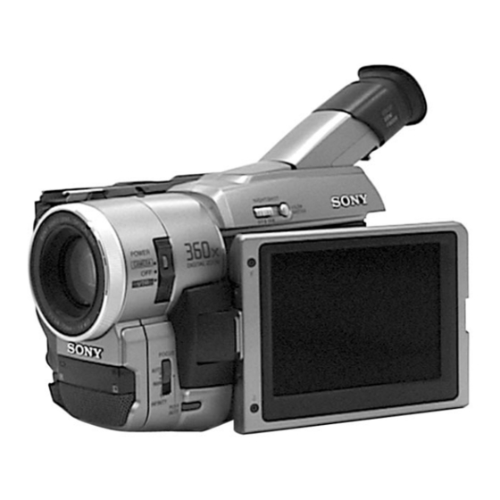
Photo: DCR-TRV510
For MECHANISM ADJUSTMENT, refer to
the "8mm Video MECHANICAL
ADJUSTMENT MANUAL
SPECIFICATIONS
DIGITAL VIDEO CAMERA RECORDER
RMT-814
US Model
Canadian Model
DCR-TRV510
AEP Model
UK Model
DCR-TRV410E/TRV510E
E Model
Hong Kong Model
Tourist Model
DCR-TRV410/TRV410E
Australian Model
Chinese Model
DCR-TRV410E
B800 MECHANISM
" (9-973-801-11).
• Abbreviation
HK : Hong Kong model
JE
: Tourist model
AUS : Australian model
CN : Chinese model
Advertisement
Table of Contents


Need help?
Do you have a question about the Digital8 DCR-TRV410 and is the answer not in the manual?
Questions and answers