Table of Contents
Advertisement
Quick Links
PCI/104-Express QSeven™ BASED SINGLE
Revision
Date
A
07/16/2014
FOR TECHNICAL SUPPORT
PLEASE CONTACT:
support@diamondsystems.com
BOARD COMPUTER
PCI/104-Express SBC with AMD Fusion G-T40E
and Integrated Data Acquisition
Rev A: July 2014
Comment
Initial Release
Copyright 2014
Diamond Systems Corporation
555 Ellis Street
Mountain View, CA 94043 USA
Tel 1-650-810-2500
Fax 1-650-810-2525
Advertisement
Table of Contents

Related Manuals for Diamond Systems PCI/104-Express QSeven


Summary of Contents for Diamond Systems PCI/104-Express QSeven
- Page 1 PCI/104-Express QSeven™ BASED SINGLE BOARD COMPUTER PCI/104-Express SBC with AMD Fusion G-T40E and Integrated Data Acquisition Rev A: July 2014 Revision Date Comment 07/16/2014 Initial Release Copyright 2014 FOR TECHNICAL SUPPORT Diamond Systems Corporation PLEASE CONTACT: 555 Ellis Street Mountain View, CA 94043 USA support@diamondsystems.com...
-
Page 2: Table Of Contents
www.diamondsystems.com CONTENTS Important Safe Handling Information ......................4 Introduction ...............................6 Functional Block Diagram ..........................8 Board Diagram ..............................9 Connector and Jumper Lists ........................11 I/O Connectors ............................11 Configuration Jumpers ..........................11 I/O Connectors ............................... 12 External Battery (J1) ........................... 12 PCI Bus (J2) ............................... 12 Input Power (J4) ............................ -
Page 3: Www.diamondsystems.com Page
13.2 Configure DIO Port Command ........................47 13.3 DIO Read ..............................48 13.4 DIO Output ..............................48 13.5 EEPROM Read............................49 13.6 EEPROM WRITE............................49 13.7 MTBF POWER CYCLE ..........................50 13.8 Watchdog Timeout Set ..........................51 13.9 Watchdog Trigger ............................52 13.10 Watchdog Read ............................ -
Page 4: Important Safe Handling Information
The list here describes common causes of failure found on boards returned to Diamond Systems for repair. This information is provided as a source of advice to help you prevent damaging your Diamond Systems (or any vendor’s) embedded computer boards. - Page 5 Overvoltage on analog input – If a voltage applied to an analog input exceeds the design specification of the board, the input multiplexor and/or parts behind it can be damaged. Most of our boards will withstand an erroneous connection of up to 35V on the analog inputs, even when the board is powered off, but not all boards, and not in all conditions.
-
Page 6: Introduction
2. INTRODUCTION The Quantum SBC family integrates a QSeven™ CPU computer-on-module (COM) plus a full analog and digital data acquisition circuit into a PCI/104-Express small form factor single board computer (SBC). It is available in the following model: Processor Speed Operating Model Memory... - Page 7 Up to 4 programmable PWM output lines Enhanced output current capability: +24mA maximum Bus Interfaces PCI-104 stackable I/O PCIe/104 stackable I/O 1 PCIe MiniCard socket Battery Backup Quantum contains a backup battery for the real-time clock and BIOS settings. The battery is directly soldered to the board and provides a minimum 7 year backup lifetime at 25°C.
-
Page 8: Functional Block Diagram
3. FUNCTIONAL BLOCK DIAGRAM Functional Block Diagram www.diamondsystems.com Quantum SBC User Manual Rev A Page 8... -
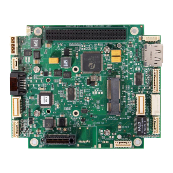
Page 9: Board Diagram
4. BOARD DIAGRAM The diagram below shows the board layout, including connectors and mounting holes. J5/J6 Quantum SBC Connector Location -- Top View www.diamondsystems.com Quantum SBC User Manual Rev A Page 9... - Page 10 Quantum SBC Connector Location -- Bottom View with QSeven COM Attached www.diamondsystems.com Quantum SBC User Manual Rev A Page 10...
-
Page 11: Connector And Jumper Lists
5. CONNECTOR AND JUMPER LISTS 5.1 I/O Connectors Connector Function External battery PCI bus LCD backlight A Input power Display port HDMI port USB1 host/client port SATA PCIe MiniCard / mSATA LCD interface channel B (LVDS format) LCD interface channel A (LVDS format) Data acquisition I/O Ethernet Audio... -
Page 12: I/O Connectors
Connector J1 is used to connect an optional external battery to replace the on-board backup battery. The on- board battery provides about 7 years of lifetime at an ambient temperature of 25⁰C. For longer lifetime an external battery of 3.3V 10% may be connected to this connector. Diamond Systems’ cable part number 6980511 mates with this connector. -
Page 13: Input Power (J4)
Quantum SBCs accept a wide-range input DC/DC power supply. This circuit accepts input voltages in the range of +6-32VDC. All other required voltages are generated on board. Each pin is rated at 3A max. Diamond Systems’ cable part number 6980510 mates with this connector. -
Page 14: Hdmi (J6)
Connector J9 is used to connect a VGA monitor. Although the DDC serial detection pins are present, a 5V power supply is not provided, and the legacy “Monitor ID” pins are also not used. Diamond Systems’ cable part number 6980507 mates with this connector. -
Page 15: Sata (J10)
Connector type: Standard 2mm single row straight pin header with gold flash plating. Connector: JST BM12B-GHS-TBT 1x12 vertical SMT 6.7 SATA (J10) This connector avails the SATA connection on the carrier boards. Ground SATA 1 TX+ SATA 1 TX- Ground SATA 1 RX- SATA 1 RX+ Ground... -
Page 16: Lvds Lcd Interface (J12, J13)
Connector J13 is used to connect LVDS LCD Channel A. Connector J12 is used to connect LVDS LCD Channel B. Voltage selection for LCD can be configured on JP7. If needed, the LCD backlight can be connected to connector JP3. Diamond Systems’ cable part number 6981211 mates with these connectors for LCD connection. J13, LCD Channel A... -
Page 17: Lcd Backlight (J3, J24)
6.10 LCD Backlight (J3, J24) Connector J3 provides the backlight power for LCD Channel A Connector. J24 provides the backlight power for LCD Channel B and control for an optional LCD panel. Diamond Systems’ cable part number 6981210 mates with this connector. -
Page 18: Ethernet (J15)
Quantum provides an HDA audio circuit based on the Realtek ALC262 audio chip. The circuit offers stereo line in, stereo line out, and mono mic in connections. Diamond Systems’ cable part number 6980508 provides the 3.5 mm output and input jacks for Lineout, Mic and Line in connection. -
Page 19: Pcie/104 (J20)
6.14 PCIe/104 (J20) The PCIe/104 (J20) connector is a 1-bank version of the PCIe/104 connector, providing only the first bank of pins numbered 1-52. It offers up to two PCIe x1 lanes from ports 2 and 3 of the QSeven module (third and fourth lanes) plus up to two USB ports from ports 6 and 7 of the QSeven module (seventh and eighth ports). -
Page 20: Ps/2 Mouse And Keyboard (J21)
J7 interfaces to USB port 1. USB 2.0 provides a 480Mbps maximum data transfer rate. The shield pin on each connector is tied to system ground. Diamond Systems’ cable part number 6980504 mates with these connectors for Host. Diamond Systems’ cable part number 6980505 mates with these connectors for Client. -
Page 21: Usb (J25, J27)
There are two serial port connectors with identical pin outs. Ports 1-2 are on J26 connector and port 3 is on the bottom side right angled J29 connector. RS-422 and RS-485 pin outs apply only to ports 1 and 2. Diamond Systems’... -
Page 22: Utility Connector (J30)
6.19 Utility Connector (J30) The pin out of the utility connector is shown below along with the corresponding QSeven module connector pin. Diamond Systems’ cable number 6980509 mates with these connectors. QSeven Pin Signal Signal QSeven Pin Reset- Pwr Switch-... -
Page 23: Configuration Jumpers
7. CONFIGURATION JUMPERS The Quantum SBC contains the following configuration jumper blocks. The diagram below shows the default jumper settings. Jumper Description Battery PCI voltage configuration LCD backlight power COM 1/2 RS-232/422/485 configuration COM 1/2 RS-422/485 termination configuration LCD supply channel A & B www.diamondsystems.com Quantum SBC User Manual Rev A Page 23... -
Page 24: Battery Configuration (Jp1)
7.1 Battery configuration (JP1) Jumper block JP1 configures the battery voltage supply. Battery Jumper JP1 VBAT_IN VCC_RTC Pins 1-2 Function Jumper VIO_RTC = 3V No jumper VCC_RTC = 0V 7.2 PCI voltage configuration (JP2) Jumper block JP2 configures the voltage supply for PCI/104 add on modules. VIO_PCI Jumper JP2 VIO_PCI 3.3V... -
Page 25: Rs-232/422/485 Configuration (Jp4)
7.4 RS-232/422/485 Configuration (JP4) Use JP4 to set COM1 and COM 2 in RS-232/422/485 modes. RS-232/422/485 Jumper JP4 W_DISABLE GROUND MODE 0 GROUND MODE 2 GROUND PIC_MCLR_RESET PIC_MCLR_RC MODE 0 MODE 2 Function 3-4 jumper (Default) 5-6 Open - No jumper RS-232 Mode ( Default) (Default) 3-4 Open - No jumper... -
Page 26: Lcd Power (Jp7)
7.6 LCD Power (JP7) Jumper block JP7 configures the voltage supply for the LCD. There are labels on the board representing the jumper configurations. Available options are +3.3V input or +5V. LCD Power JP7 VLCD_ A 3.3V 3.3V VLCD_ B Function VLCD_ A = 5V VLCD_ A =3.3 (Default) -
Page 27: System Resources
8. SYSTEM RESOURCES The table below lists the default system resources utilized by the circuits on Quantuam SBC. Device I/O Address ISA IRQ ISA DMA 0x3F8 – 0x3FF – Serial Port COM1 0x2F8 – 0x2FF – Serial Port COM2 0x3E8 – 0x3EF –... -
Page 28: Video Features
If you are using DOS, the optimum CRT resolution is 640x480. This same advice may apply for a text-based Linux environment as well. Diamond Systems cable number 6980507 is used to connect a monitor to connector J9. It provides a standard DB15 female connector for a CRT. -
Page 29: Display Port (J5)
Diamond Systems offers cable part number 6981210 with the correct connector type and pin out to match the backlight power connector on Quantum SBC. The other end may need to be changed to work with your LCD backlight inverter. -
Page 30: Updating The Bios
10. UPDATING THE BIOS The BIOS image is programmed into the Quantum SBC by using the SPIFLASH utility program. 1. Create a DOS bootable mass storage device such as a USB memory stick. 2. Copy the desired BIOS image file to the boot device. 3. -
Page 31: Bios Functions
12. BIOS FUNCTIONS The BIOS on the Quantum SBC provides access to many valuable features. These instructions show how to enter the BIOS, set up features, and restore the BIOS to its default settings. The BIOS Setup utility controls BIOS settings and configures various system features. The system settings are stored in the system’s BIOS ROM. -
Page 32: Key Commands
12.2 Key Commands The BIOS Setup utility relies on a keyboard to receive user’s instructions. Use the following keys to use the utility. Note a “WARNING” shows in the left pane onscreen when making any change to the BIOS settings. 12.3 The Menus The Quantum SBC features the BIOS Setup with six menus, which are explained hereafter in this chapter. -
Page 33: Main
12.3.1 Main The Main menu displays some important BIOS and memory information and features the settings of System Date and System Time. The displayed info is: The featured settings are: www.diamondsystems.com Quantum SBC User Manual Rev A Page 33... -
Page 34: Advanced
12.3.2 Advanced Use the Advanced menu to control the system’s PCI, ACPI, IDE, USB and Super I/O. The featured settings and submenus are: www.diamondsystems.com Quantum SBC User Manual Rev A Page 34... - Page 35 PCI Subsystem Settings This submenu configures PCI, PCI-X and PCI Express. The featured settings and submenus are: ACPI Settings ACPI Settings configure the system’s ACPI (Advanced Configuration and Power Interface). The featured settings are: www.diamondsystems.com Quantum SBC User Manual Rev A Page 35...
- Page 36 IDE Configuration Select IDE Configuration to view the system’s status of IDE, i.e. the integrated device interface, a type of disk- drive interface in which the controller electronics reside on the drive itself to eliminate the need for a separate adapter card.
- Page 37 SCH3114 Super I/O Configuration SCH3114 Super I/O Configuration is a submenu to configure the system’s Super IO chip SMSC SCH3114 to optimize the serial ports on the system. The featured submenus are: www.diamondsystems.com Quantum SBC User Manual Rev A Page 37...
-
Page 38: Chipset
12.3.3 Chipset This menu configures the system’s chipset features including bus speed management, graphics and the access to the system memory. The chipset also coordinates the communications with the PCI bus. The featured submenus are North Bridge, North Bridge LVDS Config Select, and South Bridge which are explained in the following of this section. - Page 39 GFX Configuration This submenu features the following settings to configure the system’s graphics: www.diamondsystems.com Quantum SBC User Manual Rev A Page 39...
- Page 40 Memory Configuration This submenu features the following settings to configure the system’s memory: Socket 0 Information Socket 0 Information enables viewing the CPU’s Socket 0 information such as the starting/ending address and the presence or absence of memory modules in the DIMM slots. www.diamondsystems.com Quantum SBC User Manual Rev A Page 40...
- Page 41 North Bridge LVDS configuration Select This submenu features the following settings to configure the INT15 options for the LVDS: South Bridge Select this submenu to view the south bridge’s CIM version and to configure its features. www.diamondsystems.com Quantum SBC User Manual Rev A Page 41...
- Page 42 SB SATA Configuration Use this submenu to configure the system’s SATA feature by the following settings: SB USB Configuration Use this submenu to configure the system’s USB features: www.diamondsystems.com Quantum SBC User Manual Rev A Page 42...
-
Page 43: Boot
12.3.4 Boot The Boot menu configures how to boot the system by defining boot device priority. The settings are: www.diamondsystems.com Quantum SBC User Manual Rev A Page 43... -
Page 44: Security
12.3.5 Security The Security menu sets up an administrator password to limit access to the BIOS Setup utility. Users will be asked for the password each time he/she tries to access the BIOS Setup utilities. The setting is: www.diamondsystems.com Quantum SBC User Manual Rev A Page 44... -
Page 45: Save & Exit
12.3.6 Save & Exit The Save & Exit menu features a handful of commands to launch actions from the BIOS Setup utility regarding saving changes, quitting the utility and recovering defaults. The settings are: www.diamondsystems.com Quantum SBC User Manual Rev A Page 45... -
Page 46: Pic Microcontroller
PIC MICROCONTROLLER The Quantum SBC contains a PIC microcontroller that is used to provide various functions including serial port configuration, general purpose I/O lines, A/D lines, pulse width modulators, generate wake events, and others. This section describes the command sets that can be used to communicate with the PIC controller. The list below describes the constants that have been used in this section. -
Page 47: Are You There
13.1 Are you there Command Description: Byte Length Value and Description MESSAGE_SIG: Message signature COMMAND_AREYOU: Command id for the “are you there command” 0: No extra data sent Response: Byte Length Value and Description MESSAGE_SIG: Message signature COMMAND_RECEIVER_AREYOUTHERE Specifies the length of the buffer as 1 byte long Version Number of the firmware Comments: This command is used to retrieve the firmware version running on the target system. -
Page 48: Dio Read
13.3 DIO Read Command: Byte Length Value and Description MESSAGE_SIG: Message signature COMMAND_DIO_READ: Command id for the message Response: Byte Length Value and Description MESSAGE_SIG: Message signature COMMAND_RECEIVER_DIODATA: Command id for the message 2: Indicating 2 bytes data The state of all the DIO pins from 0 to 9 Comments: This command reads the data from all the pins starting from 0 and ending with 9. -
Page 49: Eeprom Read
13.5 EEPROM Read Command: Byte Length Value and Description MESSAGE_SIG: Message signature COMMAND_READ_EPROM: Command id of the message 2: Indicating the 2 byte address to be read from the EEPROM Contains the address to be read Response: Byte Length Value and Description MESSAGE_SIG: Message signature COMMAND_RECEIVER_EPROMDATA: Indicating the following data is from reading EEPROM data 1: Indicating one byte of data to be read... -
Page 50: Mtbf Power Cycle
Comments: This command is used to write data to the EEPROM. The first four bytes will contain the data, just like other commands, only the command id and length will be different. The firmware has to know the address of the memory location where data will be written and the data itself. -
Page 51: Watchdog Timeout Set
13.8 Watchdog Timeout Set Command: Byte Length Value and Description MESSAGE_SIG: Message signature COMMAND_WATCHDOG_SET: Sets the watchdog timeout to predefined values 1: Indicating 1 byte of data follows The time value set depending on the following set of values: Value Time interval 1 sec 2 sec... -
Page 52: Watchdog Trigger
13.9 Watchdog Trigger Command: Byte Length Value and Description MESSAGE_SIG: Message signature COMMAND_WATCHDOG_TRIGGER 0: Indicating no data is sent Response: Byte Length Value and Description MESSAGE_SIG: Message signature COMMAND_RECEIVER_ACK: Command id for the message Return status command Operation completed successfully 1: Some problem in the operation Comments: The first three bytes contains data just like the previous commands. -
Page 53: Mtbf Power Data
Response: Byte Length Value and Description MESSAGE_SIG: Message signature COMMAND_RECEIVER_WATCHDOG_SETTINGS: Response ID 0: Indicating no data is sent The time value set depending on the following set of values: Value Time interval 1 sec 2 sec 4 sec 8 sec 16 sec 32 sec 1 min. -
Page 54: Rtc Read
13.12 RTC Read Command: Byte Length Value and Description MESSAGE_SIG: Message signature COMMAND_RTC_READ 0: Indicating no data is sent Response: Byte Length Value and Description MESSAGE_SIG: Message signature COMMAND_RECEIVER_RTC_DATA: Indicating the command to process 7: Specifying 7 bytes following 0 – 99 specifying the year’s last two digits 1 –... -
Page 55: Rtc Write
13.13 RTC Write Command: Byte Length Value and Description MESSAGE_SIG: Message signature COMMAND_RTC_WRITE 7: Specifying 7 bytes following this 0 – 99 specifying the year’s last two digits 1 – 12 specifying Month: 1 for January, 3 for March, 11 for November, and so on 1 –... -
Page 56: Set Com Mode
13.14 Set COM Mode Command: Byte Length Value and Description MESSAGE_SIG: Message signature COMMAND_SET_COM_MODE 1: Indicating 1 more byte to be read Indicates RS-232 protocol used Indicates RS-485 protocol used 3: SPI (Serial Peripheral Interface) protocol to be used Response: Byte Length Value and Description... -
Page 57: Read Analog Data
13.16 READ ANALOG DATA Command: Byte Length Value and Description MESSAGE_SIG: Message signature COMMAND_ANALOG_READ: Command ID 0: Indicating no data Response: Byte Length Value and Description MESSAGE_SIG: Message signature COMMAND_RECEIVER_ANALOG_DATA: Response ID 8: Indicating 8 bytes of data 8 bytes of data buffer containing the analog values for channels 0 to 3 Comments: This command retrieves the analog voltage values of channels 0 to 3. -
Page 58: Board Voltages
13.17 BOARD VOLTAGES Command: Byte Length Value and Description MESSAGE_SIG: Message signature COMMAND_BOARD_VOLTAGE: Command ID 0: Indicating no data Response: Byte Length Value and Description MESSAGE_SIG: Message signature COMMAND_RECEIVER_BOARD_VOLTAGE: Command ID 10: Indicating 10 bytes of data Comments: This command retrieves the analog voltage values of channels 6 to 10. The response consists of eight bytes of data which contain the analog voltage for channels 6 to 10 in hex. -
Page 59: Pwm Control
13.18 PWM CONTROL Command: Byte Length Value and Description MESSAGE_SIG: Message signature COMMAND_CONFIG_PWM: Command ID 4: Indicating 4 bytes of data 4 bytes of data: channel number, 2 bytes of frequency, duty cycle percentage between 0 to 100 Response: Byte Length Value and Description MESSAGE_SIG: Message signature... -
Page 60: Read Dio Config
13.19 READ DIO CONFIG Command: Byte Length Value and Description MESSAGE_SIG: Message signature COMMAND_CONFIG_READ_DIOPORT : Command ID 0: Indicating no data Response: Byte Length Value and Description MESSAGE_SIG: Message signature COMMAND_RECEIVER_CONFIG_READ_DIOPORT : Command ID 2: Indicating 2 bytes of data Comments: This command reads the configuration direction for all the pins starting from pin 0 and going to pin 9. -
Page 61: System Reset
14. SYSTEM RESET The Quantum SBC contains a soft reset switch, SW1, and hard reset switch, SW2, to reset the system under defined conditions. Reset occurs when any of the following occurs. User causes reset with SW1 or SW 2 Input voltage drops below 4.75V A system reset will also cause a reset to any installed add on modules. -
Page 62: Application Navigation
15.2 Application Navigation Figure 2: Main UI The application is created as a tabbed dialog based user interface. Each page in the application performs related task of a particular module. For sequential navigation between the pages the Previous and Next button can be used. -
Page 63: Are You There
15.3 Are You There Figure 3: Are You There screen The “Are You There” page gives information regarding the version of the firmware which is built into the target system. To get the information click on the “Are you there” button and the corresponding message will be displayed on the bottom section of the window. -
Page 64: Digital I/O
15.4 Digital I/O Figure 4: Digital I/O screen This section deals with digital input and output of the target system. There are two main operations can be performed on the digital I/O port; configure, and toggling a pin state from HIGH to LOW or LOW to HIGH. There are two columns: The first column consists of buttons to configure the corresponding DIO pin as IN/OUT direction. -
Page 65: Eeprom Access
15.5 EEPROM Access Figure 5: EEPROM Access screen This module performs operations on the EEPROM of the target system. EEPROM is the non-volatile memory module of the target system. If the user wants to store data that persists after power off of the system then this module should be used. -
Page 66: Analog Data
15.6 Analog Data Figure 6: Analog Data section This section reads data from an analog channel at regular intervals and displays the data in Voltage in the “Voltage” column and in hex value in the “Data” column. The interval for successive readings can be set using the “Enter delay”... -
Page 67: Mtbf Data
15.7 MTBF Data Figure 7: MTBF Data Section This section contains information regarding start up information. The power cycle data box shows the number of times a reset of the watchdog timer occurred. To get the data click on the “Read Data” the counter data will be displayed in the counter field. -
Page 68: Watchdog
15.8 Watchdog Figure 8: Watchdog section The watchdog module is used for recovering from firmware errors, for example if the firmware gets stuck while performing an operation. If the watchdog is enabled, it will restart the device after there is a watchdog time out and the device will again start to function. -
Page 69: Pwm
15.9 PWM Figure 9: PWM section The pulse width modulator module (PWM) is used to generate signals with various time periods and frequency. There are four channels each of which has a textbox for frequency and a track bar for setting the duty cycle. The duty cycle can be changed dynamically by sliding the track bar when the pulse width modulator is enabled. -
Page 70: Rtc/Calendar
15.10 RTC/Calendar Figure 10: RTC/Calendar section This module can be used for setting the real time clock of the CPU and also to generate an alarm pulse at a particular time. The “RTC Data” section consists of Date and Time setting options. The date format is mm/dd/yy and the time format is “hour:min:sec”. -
Page 71: Communication Mode
15.11 Communication Mode Figure 11: Communication Mode section This section is used to set a particular communication protocol. Select the mode from the “Communication Mode” combo box and then click on “Set Mode” button to set the communication mode. On a successful operation, the following message will be displayed in the “Acknowledgement messages”... -
Page 72: Board Voltages
15.12 Board Voltages Figure 12: Board Voltages section This module reads and displays voltages from channel AN6 to AN10 at a regular interval of 2 seconds. Channel Voltage Vin ( +6 to 32VDC) 2.5V 1.5V AN10 www.diamondsystems.com Quantum SBC User Manual Rev A Page 72... -
Page 73: I/O Cables
16. I/O CABLES Diamond Systems offers Cable Kit CK-QUA-01 with cables for all I/O connectors on the board except the LCD and backlight. Some cables are also available separately. Quantum SBC Cable Kit, CK-QUA-01 Photo Cable Part Quantum SBC Number... -
Page 74: Specifications
17. SPECIFICATIONS 17.1 Processor Section (All Models) QSeven COM 1GHz AMD Fusion G-T40E On-board flash 4GB MLC flash BIOS AMI PnP Flash BIOS Cooling Heat sink SDRAM memory 2GB 1.3MHz DDR3L SDRAM soldered on board Display type 18 or /24-bit dual-channel LVDS LCD VGA CRT Display Port Display resolution... -
Page 75: Data Acquisition Section
17.2 Data Acquisition Section Analog Inputs Number of channels 4 single-ended Resolution 12-bit Input ranges Unipolar: 0-3.3V Maximum input voltage +3.3V for linear operation Digital I/O Number of I/O lines Compatibility 3.3V Input voltage Low: 0V min, 0.8V max High: 2.0V min, 4.25V max Input current +/-10μA max...
Need help?
Do you have a question about the PCI/104-Express QSeven and is the answer not in the manual?
Questions and answers