Table of Contents
Advertisement
Quick Links
init
ETX 3.0 Computer-On-Module Based on Intel
Revision
Date
1.1
7/15/09
1.3
8/17/09
FOR TECHNICAL SUPPORT
PLEASE CONTACT:
support@diamondsystems.com
ETX-N270
Comment
Initial release
Minor update
®
Atom N270
Copyright 2009
Diamond Systems Corporation
1255 Terra Bella Ave.
Mountain View, CA 94043 USA
Tel 1-650-810-2500
Fax 1-650-810-2525
www.diamondsystems.com
Advertisement
Table of Contents

Related Manuals for Diamond Systems ETX-N270


Summary of Contents for Diamond Systems ETX-N270
- Page 1 ETX 3.0 Computer-On-Module Based on Intel Atom N270 Revision Date Comment 7/15/09 Initial release 8/17/09 Minor update Copyright 2009 FOR TECHNICAL SUPPORT Diamond Systems Corporation PLEASE CONTACT: 1255 Terra Bella Ave. Mountain View, CA 94043 USA support@diamondsystems.com Tel 1-650-810-2500 Fax 1-650-810-2525 www.diamondsystems.com...
-
Page 2: Table Of Contents
CONTENTS IMPORTANT SAFE-HANDLING INFORMATION ......................3 INTRODUCTION ..............................4 Features .................................4 FUNCTIONAL OVERVIEW ..........................6 Block Diagram ...............................6 Board Dimensions, Mounting Holes, and Connectors...................7 Bus and Interface Connector Summary ......................9 ETX Bus Connectors .............................9 Other Interface Connectors ...........................9 GETTING STARTED ............................10 ETX Development Kits ..........................11 Configuring the Hardware ........................... -
Page 3: Important Safe-Handling Information
The list here describes common causes of failure found on boards returned to Diamond Systems for repair. This information is provided as a source of advice to help you prevent damaging your Diamond (or any vendor’s) embedded computer boards. -
Page 4: Introduction
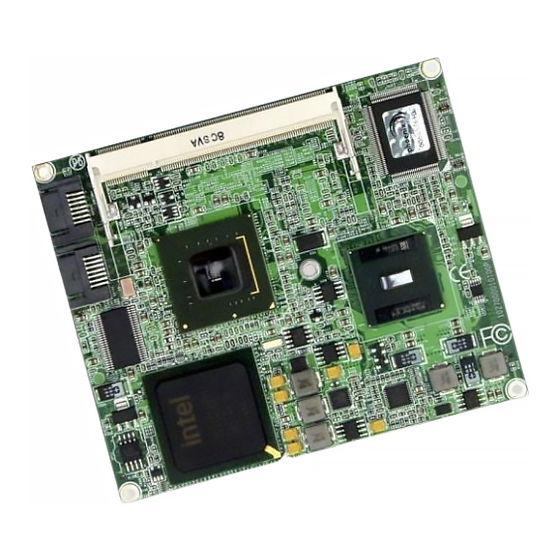
1. INTRODUCTION The ETX-N270 is a highly integrated computer-on-module (COM) based on the low power, high performance Intel Atom N270 processor clocked at 1.6GHz. The module provides an SO-DIMM socket for up to 2GB of DDR2 DRAM, and provides interface controllers for high-resolution CRT and LVDS-interfaced displays, 10/100Mbps Ethernet, SATA and IDE storage devices, USB 2.0, audio, serial, parallel, and PS/2 ports. - Page 5 USB: 4 USB 2.0 ports Other: SMbus, I C, IrDA serial interfaces PC speaker interface Watchdog timer; supports 255-level reset Dual system expansion buses: 16-bit ISA bus 32-bit PCI bus; supports 4 PCI masters Size: ETX 3.0 compliant form-factor (physical and electrical) 4.5 x 3.7 inches (95mm x 114mm) Input voltage: System power: +5V DC +/-5%...
-
Page 6: Functional Overview
2. FUNCTIONAL OVERVIEW 2.1 Block Diagram Figure 1 shows the ETX-N270 COM’s functional blocks, ETX bus, and peripheral interface signals. Figure 1: Functional Block Diagram ETX-270 User Manual 1.3 www.diamondsystems.com Page 6... -
Page 7: Board Dimensions, Mounting Holes, And Connectors
2.2 Board Dimensions, Mounting Holes, and Connectors The two diagrams below show the mechanical dimensions of the ETX-N270’s board outline and five mounting holes, as well as the position of all connectors on both the top and bottom sides of the board. - Page 8 Figure 3: Board Layout – Bottom ETX-270 User Manual 1.3 www.diamondsystems.com Page 8...
-
Page 9: Bus And Interface Connector Summary
2.3 Bus and Interface Connector Summary The ETX-N270 has seven interface connectors, as listed in the tables below. With the exception of SDVO1, these connectors are defined in accordance with the ETX 3.0 Computer-on-Module (COM) Specification. Signal functions relating to all of the module’s interface connectors are discussed in greater detail in Section 4 of this document. -
Page 10: Getting Started
3. GETTING STARTED This section of the ETX-N270 User Manual covers basic hardware setup, power connection, system boot-up, and initial software configuration. First-time ETX-N270 users normally receive the product as part of one of Diamond’s Development Kits, which provide everything needed to ensure rapid application development. -
Page 11: Etx Development Kits
Using the four long screws provided with the heat-spreader (or heatsink), secure the heat-spreader (or heatsink) to the corresponding standoffs located in the four corners of the top of the ETX-N270 module. If the ETX module is to being installed in an enclosure, align the heat-spreader’s (or heatsink’s) corner mounting ETX-270 User Manual 1.3... -
Page 12: Booting The System
The Award BIOS provides a Setup utility for specifying system configuration and settings. Pressing the <Del> key shortly after power is applied to the ETX-N270 launches the BIOS Setup utility. Watch for the following message: Press <DEL> to Enter Setup The BIOS Setup utility’s main menu provides access to the following configuration and settings pages, along with... -
Page 13: Advanced Chipset Features
3.4.3 Advanced Chipset Features From this setup page you can configure the size of the video controller’s on-chip frame buffer, set up the controller’s DVMT (Dynamic Video Memory Technology) mode and memory size, and specify what type of display will be used as the system’s boot-up console output device. DVMT is an advanced video controller function that dynamically allocates system memory to be used as video memory in order to efficiently use of available resources to maximize graphics performance. -
Page 14: Pnp/Pci Configuration
Drivers for Windows XP and Linux 2.6, if required, are included on the Software and Documentation CD that is provided along with the ETX-N270 or in its Development Kit. To locate the ETX-N270 module’s software drivers on the CD, view the index.html file in the CD’s root directory, locate “Computer-on-Modules,” and then click on “ETX-COMs.”... -
Page 15: Interface Connector Details
4. INTERFACE CONNECTOR DETAILS This section describes the functions available on all of the ETX-N270’s bus and I/O interface connectors. The ETX 3.0 specification, which provides more detail regarding the signals present on the ETX1, ETX2, ETX3, and ETX4 connectors, is available from the ETX Industrial Group’s website (http://www.etx-ig.de/specs/specs.php). -
Page 16: Etx1 Connector
4.1 ETX1 Connector The 100-pin, high-density ETX1 connector implements the board’s PCI bus, USB, and audio signals, as indicated in the table below. Further information regarding each of these signal groups follows the table. (Note: Pins designated “RESERVED” should be left unconnected.) PCICLK3 PCICLK4 SERR#... -
Page 17: Pci Bus Signals
4.1.1 PCI bus signals This set of pins implements the module’s PCI expansion bus. For further information regarding the functions of the PCI bus signals, refer to the PCI Bus Specification, available from the PCI Special Interest Group (http://www.pcisig.com/specifications). Signal Name Signal function Direction PCICLK1-4... -
Page 18: Usb Signals
4.1.2 USB signals These pins provide connections to the board’s four USB channels. For further information regarding the functions of the USB signals listed above, refer to the USB 2.0 Specification, available from the USB Implementers Forum (http://www.usb.org). Signal Name Signal Function Direction USB0+... -
Page 19: Miscellaneous Functions
4.1.4 Miscellaneous functions These pins carry power and ground signals and an interrupt request as indicated. Signal Name Signal Function Direction +5V ±5% DC power input Power ground +3.3V ± 5% supply generated on the ETX module, for powering external devices (500mA max. external load) RESERVED Do not connect SERIRQ... -
Page 20: Etx2 Connector
4.2 ETX2 Connector The 100-pin, high-density ETX2 connector implements the board’s ISA bus signals, as indicated in the table below. For further information on the module’s ISA bus signals, refer to the ETX 3.0 Specification. SD14 SD15 IRQ5 SD13 MASTER# IRQ6 SD12 DREQ7... -
Page 21: Etx3 Connector
4.3 ETX3 Connector The 100-pin ETX3 connector implements VGA, LCD (LVDS), TV-video, serial, parallel, floppy, mouse, and keyboard signals. Because pins 51-100 are shared between floppy and parallel port functions, dual signal assignments are indicated in the illustration below. Further information regarding each of these signal groups follows. -
Page 22: Analog Video Output
4.3.1 Analog video output These pins provide video, clock, and sync information for display on analog CRTs, or on LCD flat panels that are compatible with analog CRT timings, as indicated. Signal Name Signal Function Direction Horizontal sync Vertical sync Red video output Green video output Blue video output... -
Page 23: Lcd Interface
4.3.3 LCD interface These pins carry data for graphical display on an LCD panel, as indicated. Signal Name Signal Function Direction BIASON Controls display contrast voltage DIGON Controls digital power to LCD BLON# Controls backlight power to LCD LCD0-LCD19 LVDS channel data 0-19 DETECT# Panel hot-plug detection FPDDC_CLK DDC... -
Page 24: Keyboard, Mouse, And Infrared Transceiver Interfaces
4.3.5 Keyboard, mouse, and infrared transceiver interfaces These pins carry data and clock signals associated with the board’s PS2 keyboard and mouse ports. Additionally, transmit and receive data to/from an IR device, can be routed as indicated. Signal Name Signal Function Direction KBDAT Data to/from keyboard. -
Page 25: Floppy Drive Interface
4.3.7 Floppy drive interface These pins carry data and control information to/from the board’s floppy drive controller, as indicated. Signal Name Signal Function Direction LPT/FLPY# Interface configuration input RESERVED Do not connect DENSEL Diskette data density select INDEX# Index hole indicator TRK0# Track 0 indicator Write-protect indicator... -
Page 26: Miscellaneous Functions
4.3.8 Miscellaneous functions These pins carry power and ground signals and a GPIO signal, as indicated. Signal Name Signal Function Direction +5V ±5% DC power input Power ground In/Out RESERVED Do not connect LTGIO0 General purpose I/O In/Out ETX-270 User Manual 1.3 www.diamondsystems.com Page 26... -
Page 27: Etx4 Connector
4.4 ETX4 Connector The 100-pin ETX4 connector implements the board’s IDE, Ethernet, and a number of other signals, as indicated in the table below. Further information regarding each of these signal groups follows the table. SIDE_IOW# PIDE_IOR# 5V_SB PWGIN SIDE_DRQ PIDE_IOW# PS_ON# SPEAKER... -
Page 28: Ide Interfaces
4.4.1 IDE interfaces These pins carry data and control information to/from the board’s IDE drive controller, as indicated. Signal Name Signal Function Direction PIDE_D0-15 Primary IDE ATA bidirectional data bus In/Out PIDE_A0-2 Primary IDE ATA address bus PIDE_CS1# Primary IDE chip select 1 PIDE_CS3# Primary IDE chip select 3 PIDE_DRQ... -
Page 29: Ethernet Port
4.4.2 Ethernet port The ETX-N270’s 10/100Mbps Ethernet LAN interface signals on connector ETX4 require the use of an external 1:1 transformer. The ETX 3.0 specification provides further details regarding the transformer’s requirements. Signal Name Signal Function Direction TXD#, TXD Transmit data differential pair... -
Page 30: Miscellaneous Signals
4.5 SATA Connectors The ETX-N270 provides two SATA (Serial ATA) drive interfaces on a pair of 7-pin connectors located on the top side of the board. The position and pinout of each of these connectors is compliant with the ETX 3.0 Specification. -
Page 31: Sdvo Connector
4.6 SDVO Connector A low-profile 30-pin connector on the bottom of the ETX-N270 contains the set of SDVO (Serial Digital Video Out) signals generated by the ETX-N270’s IHC7-M chip. SDVO, a high-speed serial digital video interface developed by Intel, is a standard feature of many of Intel’s newest PCI Express-enabled graphics controllers. -
Page 32: Appendix: System Resources Reference
5. APPENDIX: SYSTEM RESOURCES REFERENCE 5.1 BIOS Memory Mapping Address Device Description E000:0000h - F000:FFFFh System BIOS Area D000:2000h - D000:FFFFh Free space D000:0000h - D000: FFFh LAN ROM C000:E000h - CF00:FFFFh Free space C000:0000h - C000:DFFFh VGA BIOS A000:0000h - B000:FFFFh VGA RAM 0000:0000h - 9000:FFFFh DOS 640K... -
Page 33: I/O Port Address Map
5.2 I/O Port Address Map Each peripheral device in the system is assigned a set of I/O port addresses, which also become the identity of the device. The following table lists the I/O port addresses used: Address Device Description 00000000 - 00000007 DMA Controller 00000000 - 00000CF7 PCI bus... - Page 34 000002E8 - 000002EF Communications Port (COM4) 000002F8 - 000002FF Communications Port (COM2) 00000378 - 0000037F Printer Port (LPT ) 000003B0 - 000003BB Mobile Intel 94 Express Chipset Family 000003C0 - 000003DF Mobile Intel 94 Express Chipset Family 000003E8 - 000003EF Communications Port (COM3) 000003F6 - 000003F6 Primary IDE Channel...
-
Page 35: Interrupt Request (Irq) Lines
5.3 Interrupt Request (IRQ) Lines Peripheral devices use interrupt request lines to notify CPU when services are required. The table below lists the interrupt request channels used by the ETX-N270’s onboard devices. IRQ Level Function IRQ 01 Standard 0 / 02-Key or Microsoft Natural PS/2 Keyboard... -
Page 36: Bios Post Codes
5.4 BIOS POST Codes The POST codes used by the ETX-N270’s on-board BIOS appear in the table below. Code Function Test CMOS read/write functionality Early chipset initialization: Disable shadow RAM, L2 cache (socket 7 and below), program basic chipset registers... - Page 37 Program chipset default values into chipset. Chipset default values are MODBINable by OEM customers Reserved Initial Early_Init_Onboard_Generator switch Reserved Detect CPU information including brand, SMI type (Cyrix or Intel) and CPU level ( 86 or 686) Reserved Initial interrupts vector table. If no special specified, all H/W interrupts are directed to SPURIOUS_INT_HDLR &...
- Page 38 Reserved Test 82 4 Reserved Test 82 9 interrupt mask bits for channel Reserved Test 92 9 interrupt mask bits for channel 2 Reserved Test 82 9 functionality Reserved Initialize EISA slot Reserved Calculate total memory by testing the last double last word of each 64K page; Program writes allocation for AMD K CPU Reserved Program MTRR of M CPU;...
- Page 39 Initialize Init_Onboard_Super_IO switch; Initialize Init_Onboard_AUDIO switch Reserved Okay to enter Setup utility Reserved Initialize PS/2 mouse Reserved Prepare memory size information for function call: INT h ax=E820h Reserved Turn on L2 cache Reserved Program chipset registers according to items described in Setup and Auto-Configuration table Reserved Assign resources to all ISA PnP devices;...
- Page 40 Call chipset power management hook: Recover the text fond used by EPA logo (not for full screen logo), If password is set, ask for password Save all data in stack back to CMOS Initialize ISA PnP boot devices Final USB initialization; NET PC: Build SYSID structure; Switch screen back to text mode; Set up ACPI table at top of memory;...
Need help?
Do you have a question about the ETX-N270 and is the answer not in the manual?
Questions and answers