Table of Contents
Advertisement
Quick Links
NEPTUNE Single Board Computer
EPIC Form-factor Embedded Computer with Integrated Data
Revision
Date
1.5
9/08/2009
2.0
5/13/14
2.1
5/15/15
FOR TECHNICAL SUPPORT
PLEASE CONTACT:
support@diamondsystems.com
Acquisition and Configurable CPU
Comment
Initial release
New AMD G-Series models
New Intel Bay Trail E3845 models
Copyright
Diamond Systems Corp.
555 Ellis Street
Mountain View, CA 94043 USA
Tel 1-650-810-2500
Fax 1-650-810-2525
www.diamondsystems.com
2015
Advertisement
Table of Contents

Related Manuals for Diamond Systems NEPTUNE


Summary of Contents for Diamond Systems NEPTUNE
- Page 1 NEPTUNE Single Board Computer EPIC Form-factor Embedded Computer with Integrated Data Acquisition and Configurable CPU Revision Date Comment 9/08/2009 Initial release 5/13/14 New AMD G-Series models 5/15/15 New Intel Bay Trail E3845 models Copyright 2015 FOR TECHNICAL SUPPORT Diamond Systems Corp.
-
Page 2: Table Of Contents
Software and Documentation CD ...................... 20 System Setup ............................. 21 3.2.1 Installing the Flashdisk ........................21 3.2.2 Installing the Neptune Panel I/O Board ..................... 22 3.2.3 Connecting display, keyboard, and mouse peripherals ..............22 3.2.4 Connecting Power ..........................23 Booting the System ............................ 23 Demonstrating Data Acquisition Operation .................... - Page 3 5.8.1 D/A Range ............................62 5.8.2 D/A Polarity ............................63 5.8.3 D/A Clear Select ..........................63 Neptune Baseboard I/O Register Map ......................64 Overview ..............................64 Neptune Baseboard I/O Register Summary ....................66 6.2.1 Write Register Definitions ........................66 6.2.2 Read Register Definitions ........................
- Page 4 12.1 Analog Inputs ............................117 12.2 Analog Outputs ............................117 12.3 Programmable Digital I/O Port ........................117 12.4 Optoisolated Inputs and Outputs ......................117 12.5 Counter/Timers ............................117 13. Mating Connector Reference ........................118 www.diamondsystems.com Neptune User Manual 2.1 Page...
-
Page 5: Important Safe-Handling Information
The list here describes common causes of failure found on boards returned to Diamond Systems for repair. This information is provided as a source of advice to help you prevent damaging your Diamond (or any vendor’s) embedded computer boards. - Page 6 Overvoltage on digital I/O line — The digital circuitry can be damaged if a digital I/O signal is connected to a voltage above the Neptune’s maximum specified voltage. On most of our boards the acceptable range of voltages connected to digital I/O signals is 0-5V, and they can withstand about 0.5V beyond that (-0.5 to 5.5V) before being damaged.
-
Page 7: Introduction
Neptune is offered in a range of models that vary according to the choice of ETX CPU Module, on-board SO- DIMM SDRAM capacity, +5V input or variable-input DC/DC supply, and choice of operating temperature. -
Page 8: Neptune Baseboard Features
EPIC SBC dimensions and mounting holes 1.2 Software Compatibility Neptune’s operating system compatibility depends on both the Neptune baseboard and the specific ETX CPU module attached to it. The baseboard has been qualified for use with the following operating systems: Windows XP, Windows XP Embedded SP2 Linux v2.6.23... -
Page 9: Thermal Considerations And Heatspreader
1.4 Panel I/O Board Option The ETX module’s I/O signals are available on header connectors along the edges of the Neptune baseboard. A Panel I/O Board is available that plugs into the Neptune baseboard and routes these to standard PC-style peripheral interface connectors. -
Page 10: Functional Overview
2. FUNCTIONAL OVERVIEW 2.1 Block Diagrams Figure 1 shows Neptune’s functional blocks, including circuitry contained on both the Neptune baseboard and the ETX CPU module. As indicated in the block diagram, the baseboard circuitry primarily comprises the data acquisition subsystem, gigabit Ethernet controller, DC/DC power supply, and I/O interfaces, while the ETX module integrates the system’s core embedded PC functionality. - Page 11 Figure 2: Typical ETX CPU Module Functional Block Diagram www.diamondsystems.com Neptune User Manual 2.1 Page...
-
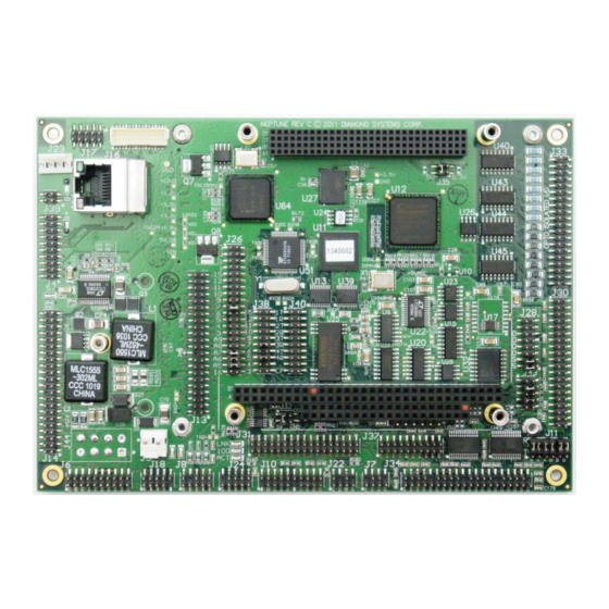
Page 12: Board Diagrams
2.2 Board Diagrams Figures 3 and 4 illustrate the location of connectors and jumpers on the top and bottom side of the Neptune baseboard. The ETX CPU module attaches on the baseboard’s bottom side, as indicated in Figure 3. Figure 3: Neptune Top View www.diamondsystems.com... - Page 13 Figure 4: Neptune Bottom View www.diamondsystems.com Neptune User Manual 2.1 Page...
-
Page 14: Interface Connector Summary
The table indicates which connectors mate with the optional Neptune Panel I/O Board (discussed elsewhere in this section), which provides standard PC-style I/O connectors. Alternatively, Diamond offers an optional Neptune Cable Kit (discussed in Section 5), which provides mating cable assemblies for most of Neptune’s I/O interface connectors. -
Page 15: Configuration Jumper Summary
2.4 Configuration Jumper Summary The Neptune baseboard’s configuration jumper blocks are listed below. Details regarding the use of these jumpers appear in Section 5 of this document. Jumper Description Serial I/O TTL/RS-232 Selection DMA / IRQ / Address Bus Configuration... -
Page 16: Getting Started
Turn on the monitor and plug in the AC Adapter. At this point, Neptune should boot-up to a Linux prompt. The above steps will be discussed in detail, after the brief overview of the Neptune Development Kit and its contents that follows. -
Page 17: Introducing The Neptune Development Kit
3.1 Introducing the Neptune Development Kit The Neptune Development Kit provides everything required for Neptune-based rapid application development. The photos and table below identify the boards, cables, and other items included in the kit. The fifteen Neptune Development Kit items pictured above are identified below. -
Page 18: Neptune Cable Kit
3.1.1 Neptune Cable Kit The Neptune cable kit (part number C-NPT-KIT) provides convenient access to all of Neptune’s I/O features. The kit’s cables are shown in the photo below and are identified in the table that follows. The components of the Neptune Cable Kit are listed below. -
Page 19: Neptune Panel I/O Board
3.1.2 Neptune Panel I/O Board The Neptune Panel I/O Board mates with the bank of connectors located along the side of the Neptune baseboard, as shown in the figures below. The board provides standard connector access for many of Neptune’s PC-style interfaces, a reset button, and a power LED. -
Page 20: 512Mb Flashdisk With Linux
An AC Adapter (P/N PS-5V-04), included in the Neptune Development Kit, converts a 110VAC to 240VAC power source to 5VDC suitable for powering a Neptune SBC. The AC Adapter’s power output cable is equipped with a connector that mates with the Neptune baseboard’s ATX-style input power connector (J44). -
Page 21: System Setup
3. Attach the female IDE connector on the flashdisk to the IDE connector J13 on the Neptune board. 4. Fasten the flashdisk in place by inserting one 2-56x pan head screw from the solder side of the Neptune board into the round spacer. -
Page 22: Installing The Neptune Panel I/O Board
2. Screw a pan head Phillips 4-40 screw through each of the two mounting holes from the top (component side) of the Panel I/O Board into the 7 mm round spacer provided on the top of the Neptune board. 3.2.3 Connecting display, keyboard, and mouse peripherals Neptune provides both VGA monitor and LVDS flat panel display interfaces. -
Page 23: Connecting Power
Connect the power output cable from the AC Adapter (P/N PS-5V-04) to its mating connector (J44) on the Neptune baseboard. At this point — with the flashdisk, Panel I/O Board, and AC Adapter installed as described above — your Neptune setup should appear as shown below. -
Page 24: Demonstrating Data Acquisition Operation
3.4 Demonstrating Data Acquisition Operation The Linux installed on the flashdisk contains software demonstration programs for Neptune’s data acquisition features. You may access the directory of these programs by typing: >cd /home/NEPTUNE The source code, makefile, and executables of the demonstration programs reside in this directory. Each demonstration program executable (and its source code) appears in its own directory. -
Page 25: Additional System Configuration
The Neptune ETX CPU module’s BIOS ROM provides a wide range of configuration options. When you power up Neptune, you can immediately enter the BIOS “Setup” utility (prior to OS boot-up) in order to adjust BIOS settings to match your system’s peripheral devices and other requirements, and to configure various other hardware and software parameters. -
Page 26: Installing The Flashdisk Programmer Board
Note: The 44-pin connectors (J1, J2, and J3) and mating cables carry +5V power, but the 40-pin connector (J4) and mating cable do not. J5 and J6 on the FDPB or J13 on the Neptune may be used to provide power to an IDE device when the device is attached to the 40-pin J4 connector on the FDPB using the Auxiliary Power Cable (DSC# 6981006) provided with the Neptune Development Kit. -
Page 27: Interface Connector Details
This set of three connectors accommodates the addition of either PC/104 (ISA bus only), PC/104-Plus (ISA and PCI buses), or PCI-104 (PCI bus only) modules on top of the Neptune baseboard. Specifications and other details on all three of these expansion module standards are available from the website of the PC/104 Consortium (http://www.pc104.org). - Page 28 IOR- SD10 DRQ6 SA16 DACK3- SD11 DACK7- SA15 DRQ3 SD12 DRQ7 SA14 DACK1- SD13 SA13 DRQ1 SD14 MASTER- SA12 REFRESH- SD15 SA11 SYSCLK Key (no pin) SA10 IRQ7 IRQ6 IRQ5 IRQ4 IRQ3 DACK2- BALE www.diamondsystems.com Neptune User Manual 2.1 Page...
-
Page 29: Pc/104-Plus Pci Bus (J3)
4.1.2 PC/104-Plus PCI Bus (J3) The Neptune baseboard’s PC/104-Plus PCI expansion bus signals are generated by the ETX CPU module, and are essentially identical in function and signaling to a normal PC motherboard’s 32-bit PCI bus except for the physical connector, a 120-pin header (J3) arranged as four 30-pin rows. Several additional pins on the PC/104- Plus connectors implement added grounds and keys. -
Page 30: Etx Utility (J4)
4.2 ETX Utility (J4) The Neptune baseboard provides a 20-pin header with access to the ETX Utility signals listed in the table below. Note: The signals on this connector’s pins are defined by the ETX CPU module. Please refer to the particular ETX module’s user manual for further details on the definition and utilization of these signals. -
Page 31: Variable Input Power (J5)
Ground 4.4 Panel I/O Board Input Power (J6) This connector provides power input from a connector located on the Neptune I/O Panel. This provides a means to power Neptune through the I/O Panel when it is packaged within an enclosure. -
Page 32: Keyboard And Mouse Ports (J7)
4.5 Keyboard and Mouse Ports (J7) Connector J7 provides signals for connection of PS/2-interfaced keyboard and mouse peripherals. This connector also mates with Neptune’s optional Panel I/O Board, resulting in its signals being routed to standard PC-style connectors. Note: The signals on this connector’s pins are defined by the ETX CPU module. Please refer to the particular ETX module’s user manual for further details on the definition and utilization of these signals. -
Page 33: Vga Display (J8)
4.6 VGA Display (J8) Connector J8 provides signals for connecting a standard VGA monitor. This connector also mates with Neptune’s optional Panel I/O Board, resulting in the VGA signals being routed to a standard PC-style connector. Note: The signals on this connector’s pins are defined by the ETX CPU module. Please refer to the particular ETX module’s user manual for further details on the definition and utilization of these signals. -
Page 34: Usb 2.0 (J10)
Connector J10 provides the data signals and power for USB ports 0–3. Each USB port supports 480 Mbps maximum transfer rates and is compliant with the USB 2.0 specification. This connector also mates with Neptune’s optional Panel I/O Board, resulting in the USB ports being routed to standard PC-style connectors. (not used) -
Page 35: Compactflash (J12)
Connector J12 — located on the bottom side of the Neptune Baseboard — is a standard 50-pin CompactFlash socket. The socket connects to Neptune’s primary IDE channel, and is configured such that the CF card is the system’s primary Master IDE device. -
Page 36: Ide (J13, J14)
CompactFlash disk on connector J12. Refer to the ETX CPU module’s user manual for further details on the signals associated with these two connectors. Reset- IDEIOW- IDEIOR- IORDY DACK- IRQ5 (not used) CBLID CS1- CS3- LED- (not used) www.diamondsystems.com Neptune User Manual 2.1 Page... -
Page 37: Lcd Lvds Interface (J16)
Connector J16 provides access to LVDS LCD display interface signals that originate on the ETX CPU module that is attached to the Neptune baseboard. Note: The signals on this connector’s pins are defined by the ETX CPU module. Please refer to the particular ETX module’s user manual for further details on the definition and utilization of these signals. -
Page 38: Lcd Lvds Control (J17)
Flat panel backlight power control VGA_DET- Flat panel hot plug detection DISP_DIGON Flat panel digital power control JILI_CLK Flat panel parameter EEPROM I C clock JILI_DAT Flat panel parameter EEPROM I C data Ground www.diamondsystems.com Neptune User Manual 2.1 Page... -
Page 39: Audio (J18)
4.12 Audio (J18) Audio connectivity is provided by connector J18. This connector also mates with Neptune’s optional Panel I/O Board, resulting in the audio signals being routed to standard PC-style connectors. Note: The signals on this connector’s pins are defined by the ETX CPU module. Please refer to the particular ETX module’s user manual for further details on the definition and utilization of these signals. -
Page 40: Utility (J22)
4.13 Utility (J22) Neptune’s Utility connector provides signals for connection of an external speaker, “power good” input, and an ATX-style power button. This connector also mates with Neptune’s optional Panel I/O Board, resulting in its signals being routed to functions on the I/O panel. -
Page 41: Hdd Power (J23)
Ground 4.15 ETX Ethernet (J24) A 10/100 Ethernet connection is provided by connector J24. This connector also mates with Neptune’s optional Panel I/O Board, resulting in the Ethernet interface being routed to a standard PC-style connector. Note: The signals on this connector’s pins are defined by the ETX CPU module. Please refer to the particular ETX module’s user manual for further details on the definition and utilization of these signals. -
Page 42: Analog I/O (J30)
(and other on-board ground/0V references). Do not assume that these grounds are floating, and do not apply a high-voltage input (relative to the power input ground) to these ground signals or to any other board I/O pin. www.diamondsystems.com Neptune User Manual 2.1 Page... -
Page 43: Digital I/O (J31)
4.17 Digital I/O (J31) Connector J31 provides the data acquisition subsystem’s programmable digital I/O signals. The signal functions are defined in the table that follows. DIN0/CLK0 DIN1/GATE0 DOUT0/CTROUT0 DOUT2/CTROUT2 AD_RCB DOUT1/SHOUT DIN3/EXTCLK DIN2/EXTGATE +5V out www.diamondsystems.com Neptune User Manual 2.1 Page... - Page 44 Pin to control gating of counters 0 and 1 for A/D timing +5V out Switched +5V power output. Caution: Do not connect this pin to an external power supply! Digital ground (0V - reference); used for digital circuitry only www.diamondsystems.com Neptune User Manual 2.1 Page...
-
Page 45: Optoisolated I/O (J33)
B5_IN A6_IN B6_IN A7_IN B7_IN Signal Definition VCC0_OUT – VCC7_OUT External voltage GND0_OUT – GND7_OUT Ground OUT0_OUT – OUT7_OUT Optoisolated outputs A0_IN, B0_IN External voltage input pairs, into FPGA . . . A7_IN, B7_IN www.diamondsystems.com Neptune User Manual 2.1 Page... -
Page 46: Com1-Com4 (J34)
Optional termination resistors for RS-422 and RS-485 operation are also selectable via jumper-group J45 (see Section 5 of this document). Connector J34 mates with Neptune’s optional Panel I/O Board, resulting in the COM1 and COM2 signals being routed to standard PC-style serial connectors. -
Page 47: Pin Assignment
Input RTSn Request to Send pin 7 Output TXDn Transmit Data pin 3 Output CTSn Clear to Send pin 8 Input DTRn Data Terminal Ready pin 4 Output Ring Indicator pin 9 Input Ground www.diamondsystems.com Neptune User Manual 2.1 Page... -
Page 48: Pin Assignment
TXD/RXD-1 COM2: TXD/RXD+2 TXD/RXD-2 COM3: TXD/RXD+3 TXD/RXD-3 COM4: TXD/RXD+4 TXD/RXD-4 Signal Definition DE-9 Pin Direction TXD/RXD+n Differential Transceiver Data (HIGH) pin 2 bidirectional TXD/RXD-n Differential Transceiver Data (LOW) pin 7 bidirectional Ground (not connected) www.diamondsystems.com Neptune User Manual 2.1 Page... -
Page 49: Pin Assignment
RXD+1 COM2: TXD+2 TXD-2 RXD-2 RXD+2 COM3: TXD+3 TXD-3 RXD-3 RXD+3 COM4: TXD+4 TXD-4 RXD-4 RXD+4 Signal Definition DE-9 Pin Direction TXD+n/TXD-n Differential transmit data Output RXD+n/RXD-n Differential receive data Input Ground (not connected) www.diamondsystems.com Neptune User Manual 2.1 Page... -
Page 50: Com5-Com6 (J37)
Connector J37 provides connectivity for serial I/O ports COM5 and COM6, which are associated with a controller on the Neptune Baseboard. RS-232 or TTL signal levels may be independently selected for these ports using jumper block J11. Unlike COM1-COM4, these two ports do not support RS-422 or RS-485 interface protocols. -
Page 51: Gigabit Led Connector (J39)
Activity LED- Speed LED 1000-/100+ Speed LED 1000+/100- 4.22 ATX-style Input Power (J44) Neptune can be connected to an external power supply via connector J44. Refer to the table below for a description of each pin’s function. PS_ON +5V standby... -
Page 52: Atx-Style Input Power Considerations
4.22.1 ATX-style Input Power Considerations The Neptune baseboard and its attached ETX CPU module can be operated from a power supply voltage of +4.75 to +5.25 VDC supplied via its ATX-style power input connector (J44), with a few restrictions. The “+12V in” power supply input provides a “pass through” power option for use with various peripherals and add-on modules. -
Page 53: Sata (Sata1, Sata2)
Connector LPC1 is located on the top of the AMD ETX computer-on-module. It is a Hirose FPC12-14P-P0.5 connector with the pin out as shown below. LAD0 LAD1 LAD2 LAD3 LFRAME# INT_SERIRQ BUF_PLT_RST# PCLK_CONN +3.3V +3.3V www.diamondsystems.com Neptune User Manual 2.1 Page... -
Page 54: Ddi (Ddi1)
Connector DDI1 is located on the top of the AMD ETX computer-on-module. It is a Hirose FH12-26S-0.5SH connector with the pin out as shown below. DDI_TX0+ DDI_TX0- DDI_TX1+ DDI_TX1- DDI_TX2+ DDI_TX2- DDI_TX3+ DDI_TX3- DDI_AUX+ DDI_AUX- DDI_HPD SMB_DAT SMB_CLK +3.3V +3.3V www.diamondsystems.com Neptune User Manual 2.1 Page... -
Page 55: Configuration Jumper Details
5. CONFIGURATION JUMPER DETAILS This section describes the use of the Neptune Baseboard’s configuration jumper options and indicates the default settings when appropriate. 5.1 Serial I/O TTL/RS-232 Selection (J11) Jumper J11 is used for selecting either RS-232 or TTL levels for serial ports COM5 and COM6, connector J34. -
Page 56: Dma Level Configuration
Jumper J26 pins, labeled 15, 12, 11, 10, 9, 7, 6, 5, 4, and 3 are used for IRQ level configuration for data acquisition IRQ. Jumper the pin for the desired IRQ level; the pin label corresponds to the IRQ level. The figure below shows an example of setting IRQ level 10. Default setting: IRQ 10. www.diamondsystems.com Neptune User Manual 2.1 Page... -
Page 57: Base Address Selection
1A0h 1C0h 1E0h 200h 220h 240h 260h 280h 2A0h 2C0h 2E0h 300h In (default) 320h 340h 360h 380h 3A0h 3C0h 3E0h The figure below shows an example of setting a base address of 240h. www.diamondsystems.com Neptune User Manual 2.1 Page... -
Page 58: Bus Width Selection
Use jumper J26, pin labeled 16, to select the desired bus width. Bus Width Pin 16 8-bit 16-bit 5.3 Single-ended/Differential Selection (J28) Use jumper J28, pins labeled D, S, to configure single-ended and differential operation, as shown in the figure below. Default setting: Single-ended www.diamondsystems.com Neptune User Manual 2.1 Page... -
Page 59: Dio Pull-Up/Pull-Down Selection (J32)
Default setting: DIO pull-down 5.5 PCI Voltage Selection (J35) Jumper J35, as shown in the figure below, is used to configure either +5V or +3.3V PCI voltage operation. Default setting: 5V PCI Voltage Selection www.diamondsystems.com Neptune User Manual 2.1 Page... -
Page 60: Irq Selection (J38)
The jumper corresponding to the desired IRQ number must be installed for the interrupts to work on the serial ports. For example, if all the ports are to be used at IRQ5, the jumper labeled IRQ5 must be installed. Pin Label The figure below shows an example of selecting IRQ3. www.diamondsystems.com Neptune User Manual 2.1 Page... -
Page 61: Com1-Com4 / Cf Configuration (J40)
In RS-422 or RS-485 serial networks, termination resistors are normally installed at the endpoints of the cables to minimize reflections on the lines. The Neptune baseboard provides 150Ω resistors for this purpose. To enable resistor termination for a port, install jumpers in locations T and R of the configuration jumper block for the port, as shown below. -
Page 62: Dac Configuration (J43)
D/A range, programmable Unipolar/bipolar D/A clear select Default settings: “5” and ”B” jumpers installed 5.8.1 D/A Range The illustrations below show the D/A range selection options for jumper J43. Default setting: +/-5V range jumper (“5”) installed www.diamondsystems.com Neptune User Manual 2.1 Page... -
Page 63: D/A Polarity
The illustrations below show the polarity selection options for J43. Default setting: Bipolar jumper (“B”) installed 5.8.3 D/A Clear Select Jumper the “R” pin pair for clear select, as shown in the figure below. Default setting: D/A Clear/Select jumper (“R”) not present www.diamondsystems.com Neptune User Manual 2.1 Page... -
Page 64: Neptune Baseboard I/O Register Map
6. NEPTUNE BASEBOARD I/O REGISTER MAP 6.1 Overview The Neptune baseboard occupies 24 bytes in the system I/O address space. Registers 12 through 15 provide paged windows for access to additional registers without requiring additional I/O address space. The following table summarizes the register functions and base address offsets for each page. Detailed bit-by-bit descriptions for each function follow thereafter. - Page 65 Page 6 — CPLD I/O Window (Enhanced Feature Page) Base + Write Function Read Function Page 6 is a window to the CPLD I/O. This page should not be accessed in normal operation. Refer to the CPLD Specification for details. www.diamondsystems.com Neptune User Manual 2.1 Page...
-
Page 66: Neptune Baseboard I/O Register Summary
6.2 Neptune Baseboard I/O Register Summary 6.2.1 Write Register Definitions Base + Main Register Set --Start A/D Conversion-- DOUT2 DOUT1 DOUT0 DACH1 DACH0 DASIM DAGEN DA11 DA10 FIFOEN SCANEN FIFORST - RESETA RESETD INTRST ADINTE DINTE TINTE RSVD1 DMAEN CLKEN... -
Page 67: Read Register Definitions
Page 6 — CPLD I/O Window (Enhanced Feature Page) This page is a window to the CPLD I/O. Refer to the CPLD specification for details. Note: Page 4, Enhanced Feature Page, is not supported on Neptune. 6.2.2 Read Register Definitions... - Page 68 Page 6 — CPLD I/O Window (Enhanced Feature Page) This page is a window to the CPLD I/O. Refer to the CPLD specification for details. Note: Page 4, Enhanced Feature Page, is not supported on Neptune. www.diamondsystems.com Neptune User Manual 2.1...
-
Page 69: Neptune Baseboard I/O Register Description
6.3 Neptune Baseboard I/O Register Description Note: In the register descriptions below, writes to undefined bits have no effect. Reads of undefined bits return zeroes. Registers 0–11 Base+0 (Write) Start A/D Conversion Bit: Name: ADSTART ADSTART Writing any value to this register starts an A/D conversion, unless a conversion is already in progress (AD_BUSY high). - Page 70 MSB is written (see below, Base+5), the value written to that register, along with the value written to this register, are simultaneously written to the D/A chip’s load register for the selected channel. See Base+5, write for more details. www.diamondsystems.com Neptune User Manual 2.1 Page...
- Page 71 DIN2–J31, pin 32. Gate for counters 1 and 2 when GT12EN = 1 (Base+10 bit 0) DIN1–J31, pin 26. Gate for counter 0 when GT0EN = 1 (Base+10 bit 2) DIN0–J31, pin 25. Clock for counter 0 when SRC0 = 1 (Base+10 bit 1) www.diamondsystems.com Neptune User Manual 2.1 Page...
- Page 72 FIFO Depth Read-back (bit 8): Bit: Name: This register provides the current FIFO depth in the enhanced mode. In the normal mode, this register is not used. FIFO depth (bit 9). (See FIFO Threshold: Base+6, below) www.diamondsystems.com Neptune User Manual 2.1 Page...
- Page 73 This register provides the current FIFO depth corresponding to the number of samples in the FIFO. FD8-FD1 The current FIFO depth. It must be noted that the FIFO depth is the actual depth and not a number shifted as in case of the FIFO threshold. www.diamondsystems.com Neptune User Manual 2.1 Page...
- Page 74 1 = FIFO has overflowed; data has been lost. This flag is cleared on the next successful A/D read. 0 = FIFO has not overflowed since the last A/D data read. FIFOEN FIFO enable read-back. SCANEN Scan enable read-back. PAGE Read-back of the current page register setting. See register Base+8 below. www.diamondsystems.com Neptune User Manual 2.1 Page...
- Page 75 Notice that bit 2 is an enhanced feature bit. Writing to the page bits will not generate a board reset or interrupt reset, as long as those bits are kept at 0 in the data written to this register. www.diamondsystems.com Neptune User Manual 2.1 Page...
- Page 76 ADCH4-0 Current A/D channel; this is the channel currently selected on board and is the channel that will be used for the next A/D conversion (unless a new value is written to the low channel register). www.diamondsystems.com Neptune User Manual 2.1 Page...
- Page 77 Counter 2 is in turn driven by counter 1, which is driven by the clock selected by bit FREQ12 in Base+10 below. 0 = External trigger: Falling edges on the DIN3/EXTCLK pin on the I/O header generate A/D conversions. www.diamondsystems.com Neptune User Manual 2.1 Page...
- Page 78 0 = No interrupt request. DMAEN Read-back of control register bit defined, above. Read-back of P2 register bit defined at Base+8/write. CLKEN Read-back of control register bit defined, above. CLKSEL Read-back of control register bit defined, above. www.diamondsystems.com Neptune User Manual 2.1 Page...
- Page 79 (gate mode). J31 pin 32 is connected to a 10KΩ pull-up resistor. 0 = The interrupt operation begins immediately once it is set up and the selected clock source begins, with no external triggering or gating. www.diamondsystems.com Neptune User Manual 2.1 Page...
- Page 80 Note: On power-up or system reset, the board is configured for A/D bipolar mode, input range = ±5V, and gain = 1, corresponding to all zeros in this register. www.diamondsystems.com Neptune User Manual 2.1 Page...
- Page 81 SCINT1-0 Read-back of control bit described, above. Only available if enhanced features are enabled. RANGE Read-back of control bit described, above. ADBU Read-back of control bit described, above. G1-0 Read-back of control bit described, above. www.diamondsystems.com Neptune User Manual 2.1 Page...
-
Page 82: Register Definitions
CTR2D2 CTR2D1 CTR2D0 CRT2D7-0 Counter 2 data. Base+15 (Read/Write) 82C54 Control: Bit: Name: SC1-0 Counter select. RW1-0 Read/write mode. M2-0 Timer mode. Binary Coded Decimal counter. Note: For more information refer the 82C54 datasheet. www.diamondsystems.com Neptune User Manual 2.1 Page... -
Page 83: Register Definitions
DIO C7-0 on connector J31 will be set to the values in this register. When the port is in input mode, the register will read back logic levels on pins DIO BC-0. C7-C0 Port C data. www.diamondsystems.com Neptune User Manual 2.1 Page... -
Page 84: Register Definitions
Page 3 Register Definitions These registers are used to control the auto-calibration process. For user software-controlled auto-calibration, these registers are used by the Universal Driver software or the user’s software to manage the calibration process. www.diamondsystems.com Neptune User Manual 2.1 Page... - Page 85 1 = Enable cal mux and disable user analog input channels. 0 = Disable cal mux and enable user inputs. TDACEN TrimDAC Enable. Writing 1 to this bit initiates a transfer to the TrimDAC (used in the autocalibration process). www.diamondsystems.com Neptune User Manual 2.1 Page...
- Page 86 Writing 0xA7 to this register disables all enhanced features. (This is the default power-on state). Any enhanced feature currently running halts and internally clears all enhanced registers to their default state. Also, the A/D FIFO depth is set to 512. Example: outp(Base+15, 0xA7) ; Disable enhanced features www.diamondsystems.com Neptune User Manual 2.1 Page...
-
Page 87: Register Definitions
DACA7-0 LSB of address to store D/A code in D/A waveform buffer. Base+13 (Write) Waveform Buffer Address (MSB): Bit: Name: DACA9 DACA8 DACA9-8 MSB of address to store D/A code in D/A waveform buffer. www.diamondsystems.com Neptune User Manual 2.1 Page... - Page 88 WGSTRT Force the waveform generator to increment one frame. Note: Only one bit can be set to 1 at a time. Bits are processed from the MSB to the LSB. The first 1 bit determines which command is executed. www.diamondsystems.com Neptune User Manual 2.1 Page...
-
Page 89: Registers 16-23
8-byte boundaries. Necessary bits = 0 1 0 1 0 0 0 = 28 Hex An easy way to generate these bits is to divide the I/O address by 8 or shift right 3 places. www.diamondsystems.com Neptune User Manual 2.1 Page... - Page 90 OPTO_I7 OPTO_I6 OPTO_I5 OPTO_I4 OPTO_I3 OPTO_I2 OPTO_I1 OPTO_I0 OPTO-10 Optoisolated I/O input data –OPTO_I7 Optoisolated Output Data Read-back: Base+19 (Read) Bit: Name: OPTO_I7 OPTO_I6 OPTO_I5 OPTO_I4 OPTO_I3 OPTO_I2 OPTO_I1 OPTO_I0 OPTO-10 Optoisolated I/O input data –OPTO_I7 www.diamondsystems.com Neptune User Manual 2.1 Page...
- Page 91 When reading from the EEPROM, the address to read from is first written to Base+20. The program must then monitor the BUSY bit in Base+20. When the BUSY bit is 0, the program may read valid EEPROM data from this register. www.diamondsystems.com Neptune User Manual 2.1 Page...
- Page 92 Serial port registers accessed using Base+16 and Base +17 The Neptune baseboard contains nine additional registers for selecting the address and interrupt level for serial ports COM3 – COM6. These registers are accessed indirectly through the address pointer register at Base+16.
- Page 93 REGISTER # 8 Bit No. COM4 COM4 COM3 COM3 COM2 COM2 COM1 COM1 Name CFG1 CFG0 CFG1 CFG0 CFG1 CFG0 CFG1 CFG0 CFG1 CFG0 PROTOCOL RS-232 RS-422 RS-485 with Echo RS-485 without Echo www.diamondsystems.com Neptune User Manual 2.1 Page...
-
Page 94: Analog I/O Operation
16-bit binary number. The maximum value of a 16-bit binary number is 2 - 1, so the full range of numerical values that you can get from a Neptune baseboard analog input channel is 0 - 65535. The smallest change in input voltage that can be detected is 1/(2 ), or 1/65536, of the full-scale input range. -
Page 95: Ranges And Resolutions
Therefore, two different formulas are needed to convert the A/D value back to a voltage, one for bipolar ranges, and one for unipolar ranges. To convert the A/D value to the corresponding input voltage, use the following formulas, depending on bipolar or unipolar mode of operation. www.diamondsystems.com Neptune User Manual 2.1 Page... - Page 96 Given, Input range is 0–10V and A/D code is 17761. Therefore, Input voltage = (17761 + 32768) / 65536 * 10V = 7.7103V. For a unipolar input range, 1 LSB = 1/65536 * Full-scale voltage. www.diamondsystems.com Neptune User Manual 2.1 Page...
- Page 97 Input Voltage for Formula 0-5V Range -32768 0.0000V -32767 1 LSB (V / 65536) 0.153 mV / 2 - 1 LSB 4.99985V 5.0000V / 2 + 1 LSB 5.00015V 32767 - 1 LSB 9.9998V www.diamondsystems.com Neptune User Manual 2.1 Page...
-
Page 98: A/D Sampling Methods
7.4.1 Sampling Modes There are several different A/D sampling modes available on a Neptune baseboard. The desired mode is selected with the FIFOEN and SCANEN bits at the FIFO Control register (Base+7), and the ADINTE bit in the Interrupt Control register (Base+9). -
Page 99: Fifo Description
Generally, the fastest sustainable interrupt rate on the ISA bus running DOS is around 40,000 per second. Since the Neptune baseboard can sample up to 250,000 times per second, the FIFO is needed to reduce the interrupt rate at high speeds. When the interrupt routine runs, it reads multiple samples from the FIFO. -
Page 100: A/D Conversion
Wait for analog input circuit to settle Initiate an A/D conversion Wait for the conversion to finish Read the data from the board Convert the numerical data to a meaningful value Each of these steps is discussed in detail, below. www.diamondsystems.com Neptune User Manual 2.1 Page... -
Page 101: Select The Input Channel
7.5.1 Select the Input Channel The Neptune baseboard contains a channel counter circuit that controls which channel is sampled on each A/D conversion command. The circuit uses two channel numbers called the low channel and high channel. These are stored in the A/D Low Channel and A/D High Channel registers (Base+2 and Base+3). The circuit starts at the low channel and automatically increments after each A/D conversion until the high channel is reached. -
Page 102: Select The Input Range
Alternatively, the value can be read as one 16-bit value, which is preferred since this method increases overall system bandwidth while reading data from the FIFO. For example: Data = inpw(base); // Where the MSB and LSB are read in one access www.diamondsystems.com Neptune User Manual 2.1 Page... -
Page 103: Convert The Numerical Data To A Meaningful Value
A/D channel range (low channel, high channel). On Neptune, the channel numbers range from 0 to 31. Some channel numbers may not be available, depending on the single-ended/differential configuration mode as explained on page 11. During interrupt- based A/D conversions, the channels being sampled must be consecutive in number. To sample only a single channel, set the low channel and high channel to the same channel number. -
Page 104: D/A Conversion
7.6 D/A Conversion Neptune uses a 4-channel 12-bit D/A converter (DAC) to provide four analog outputs. A 12-bit DAC can generate output voltages with the precision of a 12-bit binary number. The maximum value of a 12-bit binary number is - 1, so the full range of numerical values that the DACs support is 0–4095. -
Page 105: Full-Scale Range Selection
Full-scale Range Selection The D/A converter chip on Neptune requires two references, one for the low end and one for the high end of the range. The high end can be set to 5V, 10V, or Programmable, and the low end can be either 0V (for unipolar output ranges) or minus the high-end voltage. - Page 106 Round this up to 3277. (Binary value = 1100 1100 1101) Compute LSB and MSB. LSB = 3277 & 255 = 205 (Binary value = 1100 1101) MSB = int(3277/256) = 12 (Binary value = 1100) www.diamondsystems.com Neptune User Manual 2.1 Page...
- Page 107 //select page 3 outp(Base + 15, 0xA6); //enable enhanced features outp(Base + 4, LSB); outp(Base + 5, MSB); Monitor DACBUSY bit in the Status/Auxiliary Digital Input register (Base + 4). while (inp(Base + 4) & 0x80); www.diamondsystems.com Neptune User Manual 2.1 Page...
-
Page 108: Waveform Generator
4 bit depth value of waveform buffer WGCH1-0 Number of codes to output in each frame WGINC Increment by one frame WGRST Reset the waveform generator WGPS Pause/Stop the waveform generator WGSTRT Begin or resume waveform generator www.diamondsystems.com Neptune User Manual 2.1 Page... -
Page 109: Programming The D/A Waveform Generator
Input source is set on using the Waveform Generator Control register (Base+14) WGSRC0 and WGSRC1 bits. The number of the code per frame determines the number of buffer values that will be output per frame. Each code is determined by the value set at its address. www.diamondsystems.com Neptune User Manual 2.1 Page... -
Page 110: Start D/A Waveform Generator
Background The Neptune auto-calibration circuit uses an octal 8-bit TrimDAC IC to provide small adjustments to the offset and gain at various points in the circuit. Four of the DACs are used for the A/D calibration, and the other four are used for the D/A. -
Page 111: Performing Auto-Calibration With Software
Performing Auto-calibration with Software The Universal Driver software (v6.00 or later) provides two functions, dscADAutocal() and dscDAAutocal() API support for Neptune board, which can be called from within a user program to calibrate the board at any time. 8. DIGITAL I/O OPERATION... -
Page 112: Mode 0 Digital I/O
OUT1/SHOUT (pin 30) — This pin is always the value written to OUT1 bit of the Auxiliary digital Output register (Base+1). OUT0/CTROUT0 (pin 27) — The function of this pin is determined by OUT0EN bit of the Counter/Timer and DIO Control register (Base+10). www.diamondsystems.com Neptune User Manual 2.1 Page... -
Page 113: Inputs
DIO Control register (Base+10). When used as a clock for Counter 0, the rising edge is active. 8.3 Optoisolated I/O The Neptune baseboard provides 8 optoisolated (opto) I/O lines for achieving isolation. These signals are available on connector J33. The optoisolated I/O circuit is accessed through the read/write register Base+19 in page 0. -
Page 114: Counter/Timer Operation
9. COUNTER/TIMER OPERATION The Neptune baseboard’s counter/timer circuit emulates an 82C54 counter/timer chip, providing three 16-bit counter/timers. The control registers associated with D/A conversions are provided below for reference. The registers for counter/timer are in Page 0. Base + CTR0D7... -
Page 115: Counter/Timer Access And Programming
ETX COM module’s User Manual. 11. EEPROM OPERATION Neptune provides an EEPROM for storage of the address and interrupt level settings for each serial port. The EEPROM is pre-programmed with the factory default values indicated in the following table. -
Page 116: How To Use The Eeprom
Read data from the EEPROM Data register (Base+21). 11.2.3 EEPROM Reload Operation Set the RELOAD bit in the Reload Command register (Base+22) to initiate Reload operation. Monitor the BUSY bit in the EEPROM Busy Status register (Base+20) until it is 00. www.diamondsystems.com Neptune User Manual 2.1 Page... -
Page 117: Data Acquisition Subsystem Specifications
8 inputs: 5-24V 8 outputs: 5-24V 12.5 Counter/Timers Clock source: 10MHz on-board clock or external signal A/D pacer clock: 24-bit down counter (2 82C54 counters cascaded) General purpose: 16-bit down counter (1 82C54 counter) www.diamondsystems.com Neptune User Manual 2.1 Page... -
Page 118: Mating Connector Reference
The following table lists the on-board connectors and optional interface cables associated with the each of the Neptune baseboard’s I/O interfaces and expansion buses. Note: Ready-to-use interface cables for all of Neptune’s I/O connectors are available through the optional Neptune Cable Kit (Diamond part number C-NPT-KIT). Cable drawings are available on request from Diamond technical support.
Need help?
Do you have a question about the NEPTUNE and is the answer not in the manual?
Questions and answers