Advertisement
One Technology Way • P.O. Box 9106 • Norwood, MA 02062-9106, U.S.A. • Tel: 781.329.4700 • Fax: 781.461.3113 • www.analog.com
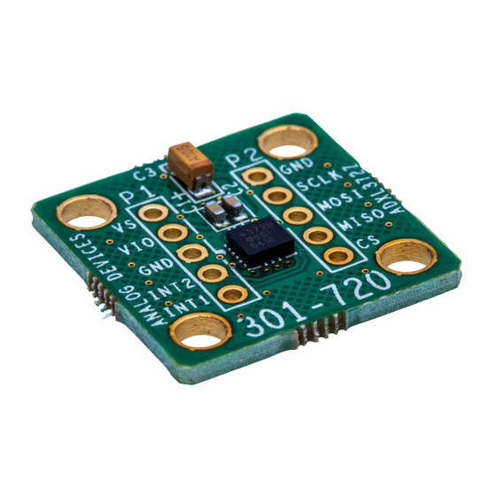
3-Axis, ±200 g Digital Accelerometer Evaluation Board
GENERAL DESCRIPTION
The
EVAL-ADXL375Z
is a simple evaluation board that allows
quick evaluation of the performance of the
digital accelerometer. The
EVAL-ADXL375Z
0.1 inch spaced vias, for population of a 4-pin and 5-pin header,
for access to all power and signal lines. The vias or headers
allow the evaluation board to be attached to a prototyping
board (breadboard) or attached to the PCB in an existing
system. Four holes are provided for mechanical attachment
of the
EVAL-ADXL375Z
to the application. An external host
processor is required for communication to the part.
The dimensions of the
EVAL-ADXL375Z
with mounting holes set 15 mm × 15 mm at the corners of the
printed circuit board (PCB).
CIRCUIT DESCRIPTION
The schematic of the
EVAL-ADXL375Z
See the
ADXL375
data sheet for configuration of the
accelerometer after it is connected to the application host
processor.
The PCB layout of the
EVAL-ADXL375Z
The
EVAL-ADXL375Z
has three factory installed capacitors for
bypass: two 100 nF capacitors and a 10 μF capacitor. C1 and C2
are V
bypass capacitors to reduce analog supply noise and C3,
S
located between V
and GND, is provided to reduce digital
DD I/O
clocking noise.
HANDLING CONSIDERATIONS
The
EVAL-ADXL375Z
is not reverse polarity protected. Reversing
the V
or V
supply and GND pins can cause damage to the
S
DD I/O
ADXL375.
Dropping the
EVAL-ADXL375Z
several thousand g's of acceleration, which may exceed the data
sheet absolute maximum limits. See the
for more information.
PLEASE SEE THE LAST PAGE FOR AN IMPORTANT
WARNING AND LEGAL TERMS AND CONDITIONS.
ADXL375
3-axis
has two sets of
are 20 mm × 20 mm
is shown in Figure 2.
is shown in Figure 1.
on a hard surface can generate
ADXL375
data sheet
EVAL-ADXL375 User Guide
EVALUATION BOARD SCHEMATIC
V
DD I/O
C3
0.1µF
GND
C2
10µF
0.1µF
V
S
CS
Rev. 0 | Page 1 of 2
EVAL-ADXL375Z
EVAL-ADXL345Z
SCL
VIO
VIO
SDA
GND
GND
345C
375Z
SDO
CS
CS
INT1
VS
VS
INT2
Figure 1. Physical Layout
ADXL375
TOP VIEW
(Not to Scale)
1
13
14
2
12
3
11
+x
4
10
+y
+z
C1
5
9
6
7
8
Figure 2. Schematic
UG-598
SCL/SCLK
SDA/SDI/SDIO
SDO/
ALT ADDRESS
INT1
INT2
Advertisement
Table of Contents

Related Manuals for Analog Devices EVAL-ADXL375


Summary of Contents for Analog Devices EVAL-ADXL375
- Page 1 EVAL-ADXL375 User Guide UG-598 One Technology Way • P.O. Box 9106 • Norwood, MA 02062-9106, U.S.A. • Tel: 781.329.4700 • Fax: 781.461.3113 • www.analog.com 3-Axis, ±200 g Digital Accelerometer Evaluation Board GENERAL DESCRIPTION EVAL-ADXL375Z EVAL-ADXL345Z EVAL-ADXL375Z is a simple evaluation board that allows...
- Page 2 By using the evaluation board discussed herein (together with any tools, components documentation or support materials, the “Evaluation Board”), you are agreeing to be bound by the terms and conditions set forth below (“Agreement”) unless you have purchased the Evaluation Board, in which case the Analog Devices Standard Terms and Conditions of Sale shall govern. Do not use the Evaluation Board until you have read and agreed to the Agreement.
Need help?
Do you have a question about the EVAL-ADXL375 and is the answer not in the manual?
Questions and answers