
Related Manuals for JAI AT-200GE


Summary of Contents for JAI AT-200GE
- Page 1 User Manual AT-200GE Digital 3CCD Progressive Scan RGB Color Camera Document Version: Ver.1.0 AT-200GE_Ver.1.0_Dec09 1014E-0912...
-
Page 2: Warranty
JAI Ltd., Japan and may only be used by the purchasers of the product. JAI Ltd., Japan makes no warranty for the use of its product and assumes no responsibility for any errors which may appear or for damages resulting from the use of the information contained herein. - Page 3 Supplement The following statement is related to the regulation on “ Measures for the Administration of the control of Pollution by Electronic Information Products “ , known as “ China RoHS “. The table shows contained Hazardous Substances in this camera. mark shows that the environment-friendly use period of contained Hazardous Substances is 15 years.
-
Page 4: Table Of Contents
JAI GigE Vision Camera operation manuals ... - 4 - Ⓡ Introduction ... - 4 - Before using GigE Vision camera ... - 5 - Software installation ... - 6 - Camera Operation ... - 6 - 1. General ... - 6 - 2. - Page 5 9.2.4 Calculation of Data Transfer Rate ... - 26 - 9.2.5 Note for 100BASE-TX connection ... - 27 - 9.3. Basic Functions ... - 27 - 9.3.1 Basic construction ... - 27 - 9.3.2 Modes of Operation ... - 28 - 9.3.3 Partial scan (Fast Dump ON) ...
-
Page 6: Jai Gige Vision Ⓡ Camera Operation Manuals
JAI SDK & Control Tool User Guide JAI SDK Getting Started Guide User’s manual is available at JAI SDK & Control Tool User Guide and JAI SDK Getting Started Guide are provided with the JAI SDK which is available at www.jai.com. Introduction GigE Vision is the new standard interface using Gigabit Ethernet for machine vision applications and it was mainly set up by AIA (Automated Imaging Association) members. -
Page 7: Before Using Gige Vision Camera
Before using GigE Vision camera All software products described in this manual pertain to the proper use of JAI GigE Vision cameras. Product names mentioned in this manual are used only for the explanation of operation. Registered trademarks or trademarks belong to their manufacturers. -
Page 8: Software Installation
The latest version of this manual can be downloaded from: www.jai.com The latest version of the JAI GigE Vision SDK & Control Tool for the AT-200GE can be downloaded from: www.jai.com For camera revision history, please contact your local JAI distributor. -
Page 9: Main Features
Analog iris video output for lens iris control LVAL synchronous/asynchronous operation (auto-detect) Comprehensive software tools and SDK for Windows XP/Vista (32 bit “x86” and 64 bit “x64” JAI SDK Ver. 1.2.1 and after ) - 7 -... -
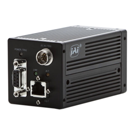
Page 10: Locations And Functions
4. Locations and Functions 4.1. Locations and Functions 1. Lens mount 2. CCD sensor 3. RJ-45 connector 4. 12-pin connector 5. D-sub 9-pin connector 6. LED 7. LINK 8. ACT 9.Holes for RJ-45 thumbscrews 10.Mounting holes *1) Note: Applicable C-mount lens should be designed for 3-CCD cameras. C-mount lens must be less than 4mm. -
Page 11: Rear Panel Indicator
4.2. Rear panel indicator The rear panel mounted LED provides the following information: Amber: Power connected - initiating Steady green : Camera is operating in Continuous mode Flashing green : The camera is receiving external trigger Ethernet connector indicates, Steady green : 1000 Base-T has been connected ... -
Page 12: Pin Assignment
Fig. 3. 12-pin connector. 5.2. Digital Output Connector for Gigabit Ethernet Type: RJ-45 HFJ11-1G02E-L21RL or equivalent The AT-200GE cameras also accept industrial RJ-45 connectors with thumbscrews. This assures that the connector does not come undone in tough industrial environments. Please recommended industrial RJ-45 connectors. -
Page 13: D-Sub 9Pin Connector (For Gpio)
5.3. D-Sub 9pin connector (For GPIO) Type : DD-09SSG Fig. 5.D Sub 9pin connector LVDS In 1- LVDS In 1+ TTL IN 1 TTL Out 1 TTL OUT 2 Note1) Can be changed by DIP switch (SW600). 5.4. DIP switch DIP switches are located on circuit boards. -
Page 14: Sw-100
5.4.2 SW-100 This switch can select the type of the signal which is output through 12-pin #10. The factory default is TTL (XEEN) and it can be changed to Open collector (EEN). Functions EEN output select Fig.7. SW100 ( 5.4.3 SW-700 This DIP switch can select OPT IN or Iris video output through pin#3 and #4 of the HIROSE 12 pin connector. -
Page 15: Input And Output Circuits
6. Input and output circuits This chapter introduces the basic diagram and bit allocation of digital output. 6.1. Iris video output This signal can be used for lens iris control In Continuous and RCT modes. The signal is NUM luminance signal and passes through the gain circuit. -
Page 16: Auto Iris Video Output Level
6.4. Auto iris video output level This video output signal is NUM luminance signal and does not have SYNC. It is available only in Continuous mode and RCT mode. It is also not available in partial scan mode. This signal is not affected by the gain control. CCD out Analog Out 200mV... -
Page 17: Gpio (General Purpose Inputs And Outputs)
7. GPIO (General purpose inputs and outputs) In chapter 7, there are some examples of settings. The values shown in these examples may need to be adjusted to fit the pixel clock specifications of this particular model. 7.1. Overview All input and output signals pass through the GPIO (General Purpose Input and Output) module. The GPIO module consists of a Look-Up Table (LUT –... -
Page 18: 12-Bit Counter
AT-200GE 7.1.2 12-bit Counter The camera pixel clock (37.125 MHz) can be used as a source. The counter has a “Divide by N”, where N has the range 1 through 4096, allowing a wide range of clock frequencies to be programmed. -
Page 19: Recommended External Output Circuit Diagram For Customer
7.2.2 Recommended External Output circuit diagram for customer Fig.15. External Output Circuit, OPT OUT 1 and 2 7.2.3 Optical Interface Specifications The relation of the Input signal and the output signal through the optical interface is as follows. Time Delay Rising TDR(µs) Rising Time RT(µs) -
Page 20: Inputs And Outputs Table
7.3. Inputs and outputs table Trigger Trigger × LVAL IN × DVAL IN × FVAL IN × EEN IN ○ OPT IN 1 ○ OPT IN 2 ○ TTL IN ○ LVDS IN ○ Soft Trigger 0 ○ Soft Trigger 1 ○... -
Page 21: Configuring The Gpio Module (Register Settings)
7.4. Configuring the GPIO module (register settings) 7.4.1 Input/Output Signal Selector GPIO is used to determine which signal is assigned which terminal. For the details, please refer to Register Map, Digital I/O, Acquisition and Trigger Control and Pulse Generator. Line Selector Line Source Line Polarity 7.4.2 12-bit counter... -
Page 22: Pulse Generators (20-Bit X 4)
“N“. The delay value is N x (1/ 25000). In the above example, the N is “0” which is no delay. The length, in this case, is 102 clocks. These settings can be achieved by using the JAI Control Tool which is the part of the JAI SDK. End Point... -
Page 23: Gpio Programming Examples
7.5. GPIO programming examples 7.5.1 GPIO Plus PWC shutter Example: 136µs unit pulse width exposure control (PWC). Pixel clock is 37.125MHz. 5049 clocks (5149-100) equals 136µs. Address 0xA040 0xB090 ① 0xB000 ② 0xB004 0xB008 0xB00C 0xB010 0xB014 0xB018 0xB060 ③ Digital I/O(GPIO) setting LVAL IN DVAL IN... -
Page 24: Internal Trigger Generator
7.5.2 Internal Trigger Generator Create a trigger signal and trigger the camera Address Register 0xA040 Trigger Mode 0xB000 Clock Choice ① 0xB004 Counter Dividing Value 0xB008 Length Counter 0 0xB00C Start point Counter 0 0xB010 Repeat Count 0 0xB014 End point Counter 0 0xB018 Counter Clear 0 0xB060... -
Page 25: Gige Vision Streaming Protocol (Gvsp)
As for the sensors in the AT-200GE, the following pixel types supported by GVSP are available. With regard to the details of GVSP, please refer to the GigE Vision Specification available from the AIA (www.machinevisiononline.org). -
Page 26: Gvsp_Pix_Rgb10V1_Packed (Rgb 32Bit Output)
9. Functions and Operations 9.1. GigE Vision Standard Interface The AT-200GE is designed in accordance with the GigE Vision standard. Digital images are transmitted over Cat5e or Cat6 Ethernet cables. All camera functions are also controlled via the GigE Vision interface. -
Page 27: Guide Line For Network Settings
Regarding data transfer rate, a larger packet size produces a slightly lower data transfer rate. The AT-200GE can support a maximum of 16020 byte packets provided the NIC being used has a Jumbo Frames function with a setting of a 16020 bytes or larger. -
Page 28: Calculation Of Data Transfer Rate
G=ROUNDUP{A*B*C/8/(E-36)}+2 Where, The following table shows bits per pixel (Item C) which depends on the pixel format. Pixel format RGB8 RGB10V1Packed RGB10V2Packed Calculation example: AT-200GE Pixel type RGB8 Item Image Width Image Height Bits per Pixel Frame Rate Packet Size Number of Packets (including Data Leader &... -
Page 29: Note For 100Base-Tx Connection
9.3. Basic Functions 9.3.1 Basic construction The AT-200GE is a 3CCD camera equipped with F4, 1/1.8-inch prism optics. Red, green and blue color signals are taken from each 2 megapixel CCD which are filtered to the red, green and blue spectral wavelengths. A 32-bit microprocessor controls all functions in the AT-200GE camera. -
Page 30: Modes Of Operation
Full scan Fig.22 Partial scan conceptual drawing The partial scan mode for the AT-200GE is variable. The first line and the last line to be read out can be set. The variable scan read out is connected with the ROI settings. - Page 31 Image Height Image start line / end line Image starts at 1st line How to calculate total line number and frame rate in variable partial scan mode Frame rate (fps) = Horizontal frequency(19.276KHz) / Total lines Total lines = ①OB period + ②Fast Dump period in the upper part of the frame (L) + ③Effective image period (L) + ④Fast dump period in the lower part of frame + ⑤Blank period (L) Where,...
-
Page 32: Vertical Binning (Vb)
Off (No V Binning)) 2:1 V Binning 9.3.5 Electronic shutter (SM) The AT-200GE has the following shutter modes. Programmable Exposure (PE) The setting command is PE and the exposure time can be controlled from 0L to 1252L in 1 LVAL units (51.88µs). -
Page 33: Auto Shutter
For an example, refer to 7.5.1 GPIO Plus PWC shutter Auto shutter The AT-200GE has an automatic shutter function which sets the video at an appropriate level depending on illumination. Auto shutter range : 1/15 sec to 1/250 sec 9.3.6 Auto-detect LVAL-sync / async accumulation... -
Page 34: Pre-Processing Functions
9.4. Pre-processing functions 9.4.1 Shading compensation The AT-200GE implements a digital shading compensation circuit for the white shading which could be caused in the prism or optical system. The whole image is divided horizontally and vertically and uses the center level as the reference. -
Page 35: White Balance
The pre-set white balance can be set to 4000K, 4600K or 5600K. The white balance of the AT-200GE is set under 7800K lighting in factory. When the camera is started up the first time, it is white balanced to 7800K and R and B gain settings are 0. -
Page 36: Blemish Compensation
The knee compensation circuit maintains linear output up to a knee point and compresses the level after the knee point. This is set by a knee slope function. The AT-200GE supports up to 200% signal compression by knee slope. Factory default is OFF. -
Page 37: Other Functions
9.5. Other functions 9.5.1 Test pattern generator (Address 0xA13C) The AT-200GE has an internal test pattern generator. These signals are output as the last process of the digital signal processing circuit and can be used for adjustment of the related system. -
Page 38: Sensor Layout And Timing
9.6. Sensor Layout and timing 9.6.1 CCD Sensor Layout Reserve 1248 1688 Optical Black Lines Active Pixels 1624(H)x1236(V) Optical Black Lines 1926Clock 1624 Read Out(Horizontal) Fig.34 CCD sensor layout - 36 - Read Out blank (Vertical) Reserve 1252 1236 blank... -
Page 39: Horizontal Timing (Normal Continuous Mode)
9.6.2. Horizontal timing (Normal continuous mode) 9.6.3 Vertical timing (Normal continuous mode) F V A L L V A L S U B E x p o s u r e P e r i o d E E N X E E N (Hi rose 12pi n) 1 0 L... -
Page 40: Horizontal Timing (Partial Scan Mode)
AT-200GE 9.6.4 Horizontal timing (Partial scan mode) Fig.37 Horizontal timing (Partial scan, the same as normal continuous) 9.6.5 Vertical timing (Partial scan mode) Fig.38 Vertical timing (Example:1/8 partial scan setting) - 38 -... -
Page 41: Horizontal Timing (Vertical Binning Mode)
Partial scan Effective lines examples 9.6.6 Horizontal timing (Vertical binning mode) Fig. 39 Horizontal timing for V binning. Total lines Horizontal Frequency 19.276 KHz 19.276 KHz 19.276 KHz 19.276 KHz - 39 - Frame rate 21.87 fps 27.69 fps 45.67 fps 68.11 fps... -
Page 42: Vertical Timing (Vertical Binning Mode)
9.6.7 Vertical timing (vertical binning mode) F VAL L VAL S UB Exposure period XEEN ( Hi rose 12pi n) 1 2 3 4 5 DATA out DVAL ▪ 1L=1LVAL period (57.54μs) ▪ OB=Optical black 9.7. Operating Modes - Timing 9.7.1 Continuous operation For applications not requiring asynchronous external triggering, this mode should be used. -
Page 43: Edge Pre-Select Trigger Mode (Eps)
9.7.2 Edge Pre-select Trigger Mode (EPS) An external trigger pulse initiates the capture, and the exposure time (accumulation time) is the fixed shutter speed set by programmable exposure or Exposure Time Abs. The accumulation can be automatically set either LVAL synchronous or LVAL asynchronous in relation to FVAL and trigger timing. - Page 44 EPS timing LVAL sync details Ext. Trigger FVAL LVAL XEEN ( Hir ose 12pi n) Exposure Period Exposure Delay t 1+1L( M ax) DATA out Fig.42 EPS timing LVAL async details Ext . Tr i g FVAL LVAL XEEN ( Hi r os e 12pi n) Exposure Exposure delay 9.
-
Page 45: Pulse Width Control Trigger Mode
9.7.3 Pulse Width Control Trigger Mode In this mode the accumulation time is equal to the trigger pulse width. Here it is possible to have a long time exposure. The accumulation can be automatically set either LVAL synchronous or LVAL asynchronous in relation to FVAL and trigger timing. The maximum recommended exposure time is <2 seconds. -
Page 46: Pwc Timing - Lval Sync Details
PWC timing - LVAL sync details Fig.45 Pulse Width Control LVAL SYNC details PWC timing - LVAL async details Ext . Tr i g FVAL LVAL XEEN ( Hi r os e 12pi n) ( Expos ur e) Del ay of Expos ur e St ar t 9. -
Page 47: Reset Continuous Trigger (Rct)
After the trigger pulse is input, a fast dump read out is performed. In the AT-200GE, this period is 7.31ms which is 141L. The exposure time is determined by the pre-set shutter speed. If no further trigger pulses are applied, the camera will continue in normal mode and the video signal is not output. -
Page 48: Sequential Trigger Mode (Eps)
9.7.5 Sequential Trigger Mode (EPS) This mode allows the user to define a preset sequence of up to 10 images, each with its own ROI, Shutter and Gain values. As each trigger input is received, the image data with the preset sequence is output as described below. -
Page 49: Delayed Readout Eps And Pwc Modes (Eps And Pwc)
Ethernet Interface. By the falling edge of the soft trigger 1, the image data is output. The AT-200GE has up to 4 frames to store, and the stored image data can be output at the consecutive timing of trigger 1. -
Page 50: Smearless Mode
AT-200GE 9.7.7 Smearless mode This function can be used to reduce the smear coming from bright areas of the image. This is effective for both EPS and PWC trigger modes. Before accumulation starts, the charge that is stored in the pixel is dumped by a high-speed transfer. This can reduce the smear that appears above the bright area but smear below the area is unaffected. -
Page 51: Optical Black Transfer Mode
Fast Dump (Partial Scan) Vertical Binning Note: The menu for ON or OFF of OB transfer mode is found in the Image Format Control section of the JAI SDK Camera Control Tool. OB Transfer Mode ON 1624 1236 1624 1624... -
Page 52: Multi Roi Mode (Multi Region Of Interest)
9.7.9 Multi ROI mode (Multi Region of Interest) In this trigger mode, up to 5 ROIs located on one image can be output by one trigger input. By using this mode, the data stream can be smaller. Each ROI can be overlapped. Please note that if the accumulated data size is bigger than the data size of 1 frame, the frame rate will be reduced. -
Page 53: External Appearance And Dimensions
AT-200GE 10. External Appearance and Dimensions Note: Rear protrusion on C-mount lens must be less than 4.0mm Fig. 52 Outline. - 51 -... -
Page 54: Specifications
11. Specifications 11.1. Camera sensitivity response Fig.53 AT-200GE Camera Sensitivity Response Wave length (nm) AT-200GE Camera sensitivity response - 52 -... -
Page 55: Specification Table
LVAL accumulation Smear less mode OB transfer mode Event message Video output connector Control interface AT-200GE 1/1.8 inch F4.0 prism Progressive 15.4 frames/second (1252 lines per frame) 37.125 MHz 19.276 kHz (1926 clk per line) 17.381 kHz (2136 clk per line) 3 x 1/1.8”... - Page 56 Note 1: Partial scan and vertical binning can not be used at the same time. Partial scan has a priority. Note 2: Above specifications are subject to change without notice Note 3: Specifications are valid after a 30 min. warm up period. AT-200GE Shutter, gain, black level, trigger mode, read out mode, GPIO setup, ROI (GenICam mandatory functions) Packet size, delayed (frame) read-out, inter-packet delay Jumbo frame can be set at max.
-
Page 57: Register Map
The content of this register map is also found in the XML file, as stipulated by the GenICam standard. Device Information Display Name Address (JAI Control Tool) 0x0048 Device Vendor Name DeviceVendoeName 0x0068... - Page 58 Binning Vertical BinningVertical 0xA13C Test Image Selector TestImageSeleector 0xA41C OB Transfer Enable OBTransferEnable Acquisition and Trigger Control Display Name Address (JAI Control Tool) 0xA604 Acquisition Mode AcquisitionMode 0xA414 Acquisition frame rate AcquisitionFrameRate 0xA000 Shutter mode ShutterMode 0xA008 Exposure Time Raw...
-
Page 59: Video Control
Trigger 0xA04C Smearless Enable SmearlessEnable LVAL Sync/Async 0xA048 LVALSyncAccumulation Accumulation Video Control Display Name Address (JAI Control Tool) 0xA050 Analog All AnalogAll 0xA054 Analog Red AnalogRed AT-200GE 25 to 64953( OFF) 25 to 64953( OFF) 25 to 64953( OFF) 0=Continuous trigger... - Page 60 Status of video processing StatusOfProcessing 0xA0D4 AWB Area Enable AWBAreaEnable 0xA17C Color Matrix Mode ColrMatrixMode AT-200GE -200 ~ 300 0 ~ 65535 0 ~ 65535 0~ 65535 Bit 16-19 AGC Area Size Bit 24-27 AGC Area Size Bit 20-23 AGC Area...
-
Page 61: Digital Processing
MatrixGB 0xA198 Matrix BR MatrixBR 0xA19C Matrix BR MatrixBG 0xA1A0 Matrix BB MatrixBB Digital Processing Display Name Address (JAI Control Tool) 0xA0F0 Gamma Set(RGB) GammaSet[RGB] Shading Correction 0xA11C ShadingCorrectionEnable Enable 0xA120 Shading Correction Mode ShadingCorrectionMode 0xA128 Blemish Reduction Enable BlemishReductionEnable... - Page 62 0xA1D0 Noise Reducer NoiseReducer 0xA1D4 Noise Reducer Threshold NoiseReducerThershold 0xA1E0 Center Marker CenterMarker Digital IO Display Name Address (JAI Control Tool) 0xA600 User Output Selector UserOutputSelector Line Selector 0xB070 Line1 Line1-TTL Out 1 Line Selector 0xB078 Line2 Line2-Optical Out 1...
-
Page 63: Pulse Generator
Line8 Line8-LVDS In Line Mode LineMode Line Format LineFormat 0xB0B0 Line status Pulse Generator Display Name Address (JAI Control Tool) 0xB004 Clock Pre-scaler ClockPreScaler 0xB008 Pulse Generator Length 0 PulseGeneratorLength0 Pulse Generator Start PulseGeneratorStartPoint 0xB00C Point 0 Pulse Generator Repeat... - Page 64 Sequence Acquisition Mode Display Name Address (JAI Control Tool) Sequence Selector SequenceSelector Sequence Exposure Time SequenceExposureTimeRa Raw to Red wRed Sequence Exposure Time SequenceExposureTimeRa 0xC000 Raw to Green wGreen Sequence Exposure Time SequenceExposureTimeRa Raw to Blue wBlue Sequence Master Gain...
- Page 65 GigE Transport Layer Display Name Address (JAI Control Tool) 0xA418 Payload size PayloadSize GigE Major Version GevVersionMajor 0x0000 GigE Minor Version GevVersionMinor GevDeviceModeIsBigEndia Is Big Endian 0x0004 GevDeviceModeCharacter Character set 0x0008 MAC address GevMacAddress GevSupportedIPConfigura Support LLA tionLLA GevSupportedConfigurati 0x0010...
- Page 66 Packet Size GevSCPSPacketSize 0x0D04 Do Not Fragment GevSCPSDoNotFragment 0x0D08 Packet Delay GevSCPD Strem Channel 0x0D18 GevSCDA Destination Address AT-200GE 0 ~4294967295 Timestamp tick frequency is 0 if timestamp is not supported. Command 2 Command 1 High 0:Open Access 1:Exclusive 2:Control 3:Exclusive Control 1476 ~16020...
-
Page 67: Event Generation
LUT Controls Display Name Address (JAI Control Tool) 0xA200 LUT Enable LUTEnable 0xD000 LUT Value (Red) LUTValue[Red] 0xD7FC 0xD800 LUT Value(Green,Bayer or Monochrome) LUTValue[Green] 0xDFFC 0xE000 LUT Value (Blue) LUTValue[Blue] 0xD7FC Event Generation Display Name Address (JAI Control Tool) Event Selector... -
Page 68: Appendix
AT-200GE Appendix 1. Precautions Personnel not trained in dealing with similar electronic devices should not service this camera. The camera contains components sensitive to electrostatic discharge. The handling of these devices should follow the requirements of electrostatic sensitive components. Do not attempt to disassemble this camera. -
Page 69: Caution When Mounting The Camera
5. Exportation When exporting this product, please follow the export regulation of your own country. 6. References 1. This manual and datasheet for AT-200GE can be downloaded from www.jai.com 2. Camera control software can be downloaded from www.jai.com 5.0mm ± 0.2mm 5.0mm ± 0.2mm... -
Page 70: Change History
Change history Date Revision Dec 2009 Changes New release - 68 -... -
Page 71: User's Record
Company and product names mentioned in this manual are trademarks or registered trademarks of their respective owners. JAI A-S cannot be held responsible for any technical or typographical errors and reserves the right to make changes to products and documentation without prior notification.
Need help?
Do you have a question about the AT-200GE and is the answer not in the manual?
Questions and answers