
Subscribe to Our Youtube Channel
Related Manuals for ADLINK Technology PCIe-9842


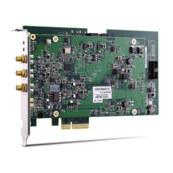
Summary of Contents for ADLINK Technology PCIe-9842
- Page 1 PCIe-9842 200 MS/s 14-Bit 1-CH High-Speed PCI Express Digitizer User’s Manual 2.00 Manual Rev. February 13, 2011 Revision Date: 50-11040-1000 Part No: Advance Technologies; Automate the World.
- Page 2 Trademarks NuDAQ, NuIPC, DAQBench are registered trademarks of ADLINK TECHNOLOGY INC. Product names mentioned herein are used for identification pur- poses only and may be trademarks and/or registered trademarks...
- Page 3 Address: 5215 Hellyer Avenue, #110, San Jose, CA 95138, USA Tel: +1-408-360-0200 Toll Free: +1-800-966-5200 (USA only) Fax: +1-408-360-0222 Email: info@adlinktech.com ADLINK Technology (China) Co., Ltd. Address: (201203) 300 Fang Chun Rd., Zhangjiang Hi-Tech Park, Pudong New Area, Shanghai, 201203 China Tel: +86-21-5132-8988 Fax:...
- Page 4 Address: 84 Genting Lane #07-02A, Cityneon Design Centre, Singapore 349584 Tel: +65-6844-2261 Fax: +65-6844-2263 Email: singapore@adlinktech.com ADLINK Technology Singapore Pte. Ltd. (Indian Liaison Office) Address: No. 1357, "Anupama", Sri Aurobindo Marg, 9th Cross, JP Nagar Phase I, Bangalore - 560078, India Tel: +91-80-65605817 Fax: +91-80-22443548 Email:...
-
Page 5: Table Of Contents
Table of Contents List of Tables................iii List of Figures ................ iv 1 Introduction ................ 1 Features................2 Applications ................. 2 Specifications............... 3 Analog Input ..............3 Timebase ................ 3 Triggers ................4 Aux Digital I/O ..............5 Data Memory ..............6 Onboard Reference ............ - Page 6 Post-Trigger or Delay-Trigger Acquisition with Re-Trigger ........... 28 Data Transfers ..............29 AUX DIO ................31 4 Calibrations ............... 33 Calibration Constant ............33 Auto-Calibration ..............34 Important Safety Instructions..........35 Table of Contents...
-
Page 7: List Of Tables
List of Tables Table 1-1: Analog Input ............. 3 Table 1-2: Timebase ..............3 Table 1-3: Triggers ..............4 Table 1-4: Aux Digital I/O ............5 Table 1-5: Data Memory ............6 Table 1-6: Onboard Reference ..........6 Table 1-7: General Information ..........7 Table 2-1: Connector Types ............ - Page 8 Figure 1-1: PCIe-9842 Product Image ......... 1 Figure 1-2: DAQPilot ..............10 Figure 1-3: DAQMaster .............. 11 Figure 2-1: PCIe-9842 Mechanical Dimensions (units in mm)... 15 Figure 3-1: PCIe-9842 Block Diagram ........19 Figure 3-2: Analog Input Signal Path ......... 20 Figure 3-3: Basic Acquisition Timing of Digitizer......
-
Page 9: Introduction
For applications that require data to be acquired and transferred in real-time, PCIe-9842 is designed on the PCI Express x4 bus as the interface. When signal is converted from analog to digital data, data will be transferred to host system memory continuously due to PCI Express high bandwidth features. -
Page 10: Features
1.1 Features Up to 200MS/s sampling rate High resolution 14-Bit ADC ±1V Input range with 50Ω input impedance and DC couple Up to 100 MHz bandwidth for analog input High dynamic performance, up to 70 dB SNR with 10 MHz ... -
Page 11: Specifications
1.3 Specifications 1.3.1 Analog Input Specification Value Number of Channels 1 single-ended channel Connector SMA Screw Type Input Impedance 50Ω ± 2% Input Coupling Input Signal Range ±1.0 V Overvoltage Protection ±5 V ADC Resolution 14 bits, 1 in 16,384 Offset Error ±1 mV Gain Error... -
Page 12: Triggers
1.3.3 Triggers Specifications Value Software trigger Trigger Source External digital trigger Post-Trigger, delay-trigger Trigger Mode Re-trigger for all trigger modes External Digital Trigger Input Compatibility 3.3 V TTL, 5 V tolerant Input High Threshold (V 2.0 V Input Low Threshold (V 0.8 V Maximum Input Overload -0.5 V to+5.5 V... -
Page 13: Aux Digital I/O
1.3.4 Aux Digital I/O Specification Value Static DIO interface Aux DIO Function Synchronized digital input interface IO Compatibility 3.3V TTL Input Level High (VIH) 2.0V minimum Input Level Low (VIL) 0.8V maximum Output Level High (VOH) 2.4V minimum Output Level Low (VOL) 0.2V maximum Output Driving Capability ±12 mA... -
Page 14: Data Memory
1.3.5 Data Memory Specification Value Onboard Memory 16K samples Data Transfer Type Scatter-gather DMA transfer Table 1-5: Data Memory 1.3.6 Onboard Reference Specification Value Recommend Warm-Up Time 15 minutes Reference Voltage +5.000 V Reference Temp. Coeff. ppm/°C <±5.0 ppm/°C Table 1-6: Onboard Reference Introduction... -
Page 15: General Information
1.3.7 General Information Specification Value Environment Ambient temperature: 0°C to +50°C Operating Environment Relative humidity: 10% to 90% non-condensing Ambient temperature: -20°C to +80°C Storage Temperature Relative humidity: 10% to 90% non-condensing Physical PCI-E: Standard PCI Express short length card PCB Dimension (not including connector) 106.7 mm (H) X 174.6 mm(W) -
Page 16: Software Support
LabVIEW® and MATLAB®. ADLINK also pro- vides ActiveX component ware measurement, breakthrough proprietary software applications. All software options are included in the ADLINK All-in-One CD. Supported Operating System Windows 7/Vista/XP Linux Recommended Application Environments VB.NET/VC.NET/VB/VC++/BCB ... -
Page 17: Wd-Dask
DAQPilot is a driver and SDK with a graphics-driven interface for various application development environments. DAQPilot comes as ADLINK's commitment to provide full support to its comprehen- sive line of data acquisition products and is designed for the nov- ice to the most experienced programmer. -
Page 18: Figure 1-2: Daqpilot
Figure 1-2: DAQPilot You can download and install DAQPilot at: http://www.adlinktech.com/TM/DAQPilot.html Introduction... -
Page 19: Daqmaster
1.4.4 DAQMaster ADLINK DAQMaster is a smart device manager that opens up access to ADLINK data acquisition and test and measurement products. DAQMaster delivers all-in-one configurations and pro- vides you with a full support matrix to properly and conveniently configure ADLINK Test and Measurement products. - Page 20 Introduction...
-
Page 21: Getting Started
Anti-static mat The ADLINK PCIe-9842 digitizer cards are electro-static sensitive equipment that can be easily damaged by static electricity. The equipment must be handled on a grounded anti-static mat. The operator must wear an anti-static wristband, grounded at the same point as the anti-static mat. -
Page 22: Package Contents
Warning:DO NOT install or apply power to equipment that is dam- aged or if there is missing/incomplete equipment. Retain the shipping carton and packing materials for inspection. Please contact your ADLINK dealer/vendor immediately for assis- tance. Obtain authorization from your dealer before returning any product to ADLINK. -
Page 23: Device Layout And I/O Connectors
2.3 Device Layout and I/O Connectors Connectors for AUX DIO Figure 2-1: PCIe-9842 Mechanical Dimensions (units in mm) Getting Started... -
Page 24: Table 2-1: Connector Types
The connector types and functions are described as follows. Mark on Name Type Remark Faceplate ON status for card registered to system LED1 Green OFF Status for card released from system BLINK status for Acquisition on- LED2 Blue going OFF status for Acquisition stop Analog Input Analog input channel... -
Page 25: Table 2-2: Auxiliary Digital I/O
The PCIe-9842 includes a connector for auxiliary DIO functions. This digital IO port serves as two functions: general purpose DIO and synchronized DI. For more detail operation of AUX DIO func- tion, please refer to Section 3. The following table depicts the pin define of this connector. -
Page 26: Installing The Module
2.4 Installing the Module To install the card: 1. Turn off the system/chassis and disconnect the power plug from the power source. 2. Remove the system/chassis cover. 3. Select the PCI slot that you intend to use, then remove the bracket opposite the slot, if any. 4. -
Page 27: Operation Theory
Operation Theory The operation theory of the PCIe-9842 is described in this chapter, including the control and setting of ADC sampling, trigger sources, trigger modes and data transfer. 3.1 Functional Block Diagram Aux DIO Port TRG IN FPGA FIFO Interface... -
Page 28: Basic Ai Acquisition
3.2 Basic AI Acquisition In this section, we are going to explain the basic acquisition timing. 3.2.1 Analog Input Path The following figure shows the block diagram of the analog input path of a digitizer. The input channel is terminated with 50 Ω input impedance. -
Page 29: Basic Acquisition Timing
3.2.2 Basic Acquisition Timing The PCIe-9842 begins acquisition process when it receives a trig- ger event. The trigger event comes from software command or external digital trigger. The Timebase is a clock that sent to the ADC and the acquisition engine for essential timing functionality. -
Page 30: Figure 3-4: Different Sampling Rate By Setting Different Scan Interval Counters
Trigger TIMEBASE ScanIntrv = 1 ScanIntrv = 2 DATA ScanIntrv = 3 Acquisition starts right after this clock edge Acquisition In Progress Figure 3-4: Different Sampling Rate by Setting Different Scan Interval Coun- ters Counter Name Length Valid Value Description Scan Interval Counter This counter is a Timebase divider to... -
Page 31: Ai Data Format
3.2.3 AI Data Format The ADC data of the PCIe-9842 is on the 14 MSB of the 16-bit A/D data. The 2 LSB of the 16-bit A/D data should be truncated by soft- ware when SDI function does not enable. When SDI function enabled, the 2 LSB, bit 0 and bit 1, represent the SDI0 and SDI1, respectively. -
Page 32: Synchronous Digital Input
3.2.4 Synchronous Digital Input The PCIe-9842 has two synchronous digital input channels, SDI0 an SDI1. These two digital input lines can be sampled synchro- nously with Timebase clock for mixed signal applications. Thus the data transfer can up to 200 Mbit/s when using internal 200 MS/s Timebase clock. -
Page 33: Trigger Sources
3.3 Trigger Sources The PCIe-9842 supports trigger signal from software command and external digital signal. When the PCIe-9842 receives a trigger, a sequence of acquisition operation begins. A software trigger is generated by a software command through API. The trigger asserts right after executing the specific API func- tion. -
Page 34: Trigger Modes
Use post-trigger acquisition when you want to collect data after the trigger event, as illustrated in Figure 3-7. When the operation starts, PCIe-9842 waits for a trigger event. Once it receives the trigger signal, the acquisition begins. Data generates from ADC and being transferred to system memory continuously. -
Page 35: Delay Trigger Acquisition
3.4.2 Delay Trigger Acquisition Use delay-trigger acquisition to delay the data collection after the trigger event, as illustrated in Figure 3-8. When PCIe-9842 receives trigger event, it waits a certain delay time and then begins acquisition. The delay time is specified by a 16-bit counter value so that the maximum delay time is the period of TIMEBASE X (2 - 1), while the minimum delay is the period of Timebase. -
Page 36: Post-Trigger Or Delay-Trigger Acquisition
3.4.3 Post-Trigger or Delay-Trigger Acquisition with Re- Trigger Use post-trigger or delay trigger acquisition with re-trigger function to collect data after several trigger events, as illustrated in Figure 3-9. You can program the number of triggers then the digitizer will acquire a specific sample data each time a trigger is accepted. -
Page 37: Data Transfers
One of the most important features of the PCIe-9842 is its PCI Express x4 interface. PCIe-9842 equips a 200MS/s high sampling rate ADC, it generates 400MByte data rate per second. Therefore it is very useful to have high bandwidth bus interface when stream- ing data from ADC to system memory. -
Page 38: Figure 3-10: Data Transfers
In a multi-user or multi-tasking OS, such as Microsoft Windows, Linux, and so on, it is difficult to allocate a large continuous mem- ory block. Therefore, the bus controller provides DMA transfer with scatter-gather function to link non-continuous memory blocks into a linked list so users can transfer large amounts of data without being limited by memory limitations. -
Page 39: Aux Dio
3.6 AUX DIO The PCIe-9842 features an auxiliary digital IO port. The auxiliary digital IO is software configurable for two functions: General purpose digital IO When configured as general purpose digital IO port, there are 8 digital lines for digital IO. Each line can be configured its direc- tion as input or output by software. - Page 40 Operation Theory...
-
Page 41: Calibrations
The PCIe-9842 is factory calibrated before shipment by writing the associated calibration constants to the onboard EEPROM. Every time the system boot up, the PCIe-9842 driver will load these cali- bration constants that minimize the error in analog input path and analog output circuit. -
Page 42: Auto-Calibration
EEPROM. Before user begins the auto-calibration procedure, it is recommended to warm up the PCIe-9842 for at least 15 minutes. Please remove cables before an auto-calibration procedure is initi- ated. -
Page 43: Important Safety Instructions
Important Safety Instructions For user safety, please read and follow all instructions, WARNINGS, CAUTIONS, and NOTES marked in this manual and on the associated equipment before handling/operating the equipment. Read these safety instructions carefully. Keep this user’s manual for future reference. ... - Page 44 Never attempt to fix the equipment. Equipment should only be serviced by qualified personnel. A Lithium-type battery may be provided for uninterrupted, backup or emergency power. RISK OF EXPLOSION IF BATTERY IS REPLACED BY AN INCORECT TYPE. DISPOSE OF USED BATTERIES ACCORDING TO THEIR INSTRUCTIONS.
Need help?
Do you have a question about the PCIe-9842 and is the answer not in the manual?
Questions and answers