Sign In
Upload
Manuals
Brands
ADLINK Technology Manuals
PCI Card
PCI-9524
User Manuals: ADLINK Technology PCI-9524 DAQ
Manuals and User Guides for ADLINK Technology PCI-9524 DAQ. We have
1
ADLINK Technology PCI-9524 DAQ manual available for free PDF download: User Manual
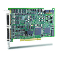
ADLINK Technology PCI-9524 User Manual (98 pages)
24-Bit Precision Load Cell Input Card
Brand:
ADLINK Technology
| Category:
PCI Card
| Size: 2 MB
Table of Contents
Revision History
2
Preface
3
Copyright 2008 ADLINK TECHNOLOGY INC
3
Environmental Responsibility
3
Trademarks
3
Using this Manual
5
Conventions
6
Acronyms & Terminology
7
Reference Documentation
10
Getting Service
11
Table of Contents
13
List of Figures
17
1 Introduction
21
Figure 1-1: PCI-9524 Product Image
21
Applications
22
Features
22
Specifications
23
Table 1-1: -3Db Small Signal Bandwidth: (Typical, 25°C)
24
Table 1-2: System Noise (Including Quantization, Typical, 25°C)
24
Table 1-3: Transducer Input Impedance
25
Table 1-4: Transducer CMRR (DC to 60 Hz, Typical 25°C)
25
Table 1-5: Settling Error: (Typical, 25°C)
26
Table 1-6: Programmable Input Range and Gain
27
Table 1-7: -3Db Small Signal Bandwidth Vs. Input Range
27
Table 1-8: -3Db Small Signal Bandwidth Vs. Sampling Rates, in ±10V Range
28
Figure 1-2: Effective-Number-Of-Bits Vs. Gain
29
Figure 1-3: RMS Noise in ΜV Vs. Gain
29
Figure 1-4: Spectral Response ±10V Range, 0.996094 Hz Sine Wave, -1 Db FS
30
Figure 1-5: Spectral Response ±5V Range, 0.996094 Hz Sine Wave, -1 Db FS
30
Figure 1-6: Spectral Response ±2.5V Range, 0.996094 Hz Sine Wave, -1 Db FS
31
Figure 1-7: Spectral Response ±1.25V Range, 0.996094 Hz Sine Wave, -1 Db FS
31
Figure 1-8: Frequency Response Sampling at 30,000 SPS
32
Figure 1-9: Frequency Response Sampling at 15,000 SPS
32
Figure 1-10: Frequency Response Sampling below 15,000 SPS
33
Table 1-10: General Purpose CMRR (DC to 60 Hz, Typical, 25°C)
33
Table 1-9: General Purpose Input Impedance
33
Table 1-11: Settling Error: (Typical, 25ºC)
34
Software Support
39
2 Getting Started
41
Installation Environment
41
Package Contents
42
ADLINK Technology Inc. PCI
43
PCI-9524 Layout
43
Figure 2-1: PCI-9524 PCB Layout and Mechanical Drawing
43
Installing the Card
44
PCI Configuration
45
3 Signal Connections
47
Connectors & Pin Assignments
47
Figure 3-1: CN1 Connector & Pin Assignments
47
Figure 3-2: CN2 Connector & Pin Assignments
49
Figure 3-3: SSI Connector & Pin Assignments
51
Table 3-1: I/O Signal Descriptions
52
Analog Input Signal Connections
53
Signal Sources
53
Input Configurations
54
Figure 3-4: Connecting to a Four-Terminal Load-Cell Transducer Using a Four-Wire Connection
54
Figure 3-5: Connecting to a Six-Terminal Load-Cell Transducer Using a Six-Wire Connection
55
Figure 3-6: Connecting to a Four-Terminal Load-Cell Transducer Using a Six-Wire Connection
56
Figure 3-7: Ground-Referenced Source and Differential Input
57
Figure 3-8: Floating Source and Differential Input
57
Isolated Digital Signal Connection
58
Signal Sources and Terminal Devices
58
Connecting To/From External Encoders
60
Figure 3-9: Connecting to an External Encoder
60
With Npn Sink Drivers
60
Figure 3-10: Connecting to an External Encoder
60
With Pnp Source Drivers
60
Figure 3-11: Connecting to an External Encoder with Push-Pull Source Drivers
61
Figure 3-12: Connecting to an External Encoder with Differential Line-Drivers
61
Connecting to External Servo Amplifiers
62
Figure 3-13: Connecting to an External Servo-Amplifier with Opto-Coupler Inputs
62
Figure 3-14: Connecting to an External Servo-Amplifier with Differential Line-Receivers
62
Interfacing Isolated DO with External Loads
63
Figure 3-15: Connecting to an External Resistive Load from the Isolated DO Sink Driver
63
Figure 3-16: Connecting to an External Inductive Load from an Isolated DO Sink Driver
64
Interfacing Isolated DI with External Devices
65
Figure 3-17: Connecting to a Low-Side Push Button
65
Figure 3-18: Connecting to an External Sink Driver
66
4 Operation Theory
67
PCI-9524 Function Diagram
67
Figure 4-1: PCI-9524 Function Diagram
67
Analog Input Channels
68
Signal Acquisition and Processing Flow
68
Figure 4-2: Signal Acquisition and Data Processing Flow for Transducer Input Channels
68
How to Define a 1 in 200,000 Count Resolution
69
Data Rate Versus Sampling Rate
71
Auto-Scan, Multiplexing and Settling Time
71
Power Line Noise Rejection
73
Table 4-1: Data Rates Vs. Multiplexing, Auto-Zero & ADC Sampling Rates, in Samples-Per-Second (SPS)
73
Excitation and Remote-Sensing
74
Figure 4-3: SINC Filter Power Line Noise Rejection at 60 Hz Multiples
74
Thermal EMF, 1/F Noise and Auto-Zero
75
Table 4-2: Temperature Coefficient of Different Metal Junctions
76
Figure 4-4: the Effect of Auto-Zero on Thermal Noise and 1/F Noise, ADC Running at 60 SPS
77
Warm-Up Requirement
78
Post-Processing IIR Digital Filter
78
Figure 4-5: Digital Filter Tap Length Effects on Signal Frequency Responses
79
10RAW Data Format
81
Table 4-3: Default Threshold Values (ADC Counts) Vs. ADC Sampling Rates
81
Table 4-4: RAW Data Format
81
11AD Data Format
82
Table 4-5: Bipolar Analog Input Ranges and Output Digital Codes for Transducer Input Channels
83
Table 4-6: Bipolar Analog Input Ranges and AD Codes for General Purpose Input Channels
83
12Data Transfer Modes
84
Figure 4-6: Linked List of PCI Address DMA Descriptors
85
13Trigger Modes
86
Figure 4-7: Post Trigger
86
D/A Conversion
87
Isolated Encoder Input Channels
87
Table 4-7: Bipolar Output Code Table
87
Figure 4-8: X4 Encoder Mode
88
Isolated Pulse-Command Generator
89
Isolated Digital I/O
89
Isolated Digital Inputs
90
Isolated Digital Outputs
90
Trigger Sources
90
Software-Trigger
90
External Digital Trigger
90
Pulse Comparator Trigger
91
Figure 4-9: External Digital Trigger
91
Position Comparator Trigger
92
5 Calibration
93
Loading Calibration Constants
93
Auto-Calibration
94
Saving Calibration Constants
94
Important Safety Instructions
95
Warranty Policy
97
Advertisement
Advertisement
Related Products
ADLINK Technology NuDAQ PCI-9111DG
ADLINK Technology NuDAQ PCI-9111HR
ADLINK Technology NuDAQ PCI-9114DG
ADLINK Technology NuDAQ PCI-9114HG
ADLINK Technology NuDAQ PCI-9812/10
ADLINK Technology NuDAQ PCI-9810
ADLINK Technology NuDAQ PCI-9812
ADLINK Technology NuDAQ PCI-9112
ADLINK Technology NuDAQ PCI-7396
ADLINK Technology PCI-7234
ADLINK Technology Categories
Computer Hardware
Motherboard
PCI Card
Control Unit
Desktop
More ADLINK Technology Manuals
Login
Sign In
OR
Sign in with Facebook
Sign in with Google
Upload manual
Upload from disk
Upload from URL