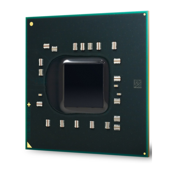
Intel Core 2 Duo Processor User Manual

Intel Core 2 Duo Processor User Manual

Development kit with ddr3 system memory
Hide thumbs Also See for Core 2 Duo Processor:
Table of Contents

Advertisement

®
TM
Intel
Core
2 Duo Processor
®
and Intel
GM45 Express Chipset
(with DDR3 System Memory)
Development Kit User's Manual
September 2008
Document Number: 320249-001

Advertisement

Table of Contents
loading

Summary of Contents for Intel Core 2 Duo Processor

  • Page 1 ® Intel Core 2 Duo Processor ® and Intel GM45 Express Chipset (with DDR3 System Memory) Development Kit User’s Manual September 2008 Document Number: 320249-001...
  • Page 2 Contact your local Intel sales office or your distributor to obtain the latest specifications and before placing your product order. Copies of documents which have an order number and are referenced in this document, or other Intel literature may be obtained by calling 1-800-548-4725 or by visiting Intel's website at http://www.intel.com.
  • Page 3: Table Of Contents

    Contents Introduction .....................8 Content Overview...................8 Text Conventions ...................9 Glossary of Terms and Acronyms ............10 Development Kit Technical Support ............14 1.4.1 Online Support................14 1.4.2 Additional Technical Support .............14 Related Documents................15 1.5.1 Ordering Hard Copies of Documents...........15 Getting Started....................17 Overview ....................17 Development Kit Contents ..............17 Additional Required Hardware (Not Included in the Development Kit)...18 Additional Required Software (Not included in the Development Kit) ....
  • Page 4 Rework to Change Eaglemont Card from HDMI to Display Port ..60 A.3.2 AUX Pull Down Rework.............62 Intel® High Definition Audio Interposer Card (Mott Canyon 4) (Not Included)63 A.4.1 Mott Canyon 4 Jumper Settings ..........64 ExpressCard Module Interposer (Duck Bay 3) (Not Included) ......66 PCI Express Mini Card Interposer (Upham IV) (Not Included)......67...
  • Page 5 Appendix C Programming System BIOS Using a Flash Programming Device ......74 Appendix D CPU Thermal Solution (Heatsink) Installation ............75 Figures Figure 1. Development Board Block Diagram............25 Figure 2. Silver Cascade Development Board Components ........46 Figure 3. Back Panel Connectors ...............48 Figure 4.
  • Page 6 Table 1. Text Conventions ..................9 Table 2. Definitions of Terms ................10 Table 3. Acronyms ..................11 Table 4. Related Documents ................15 Table 5. Intel Literature Centers................15 Table 6. Development Board Feature Set Summary ..........26 Table 7. TV–Out Connections ................32 Table 8. PCI Express Ports................33 Table 9.
  • Page 7: Revision History

    Revision History Document Revision Description Revision Date Number Number 320249 Public launch release September 2008 Note: The differences between the Pillar Rock (DDR2) and Silver Cascade (DDR3) User Guides are in the DDR2 vs. DDR3 memory controller interface, the Configuration Jumpers and Switches Settings Table and the Development Board Components Table.
  • Page 8: Introduction

    It gives a descript ion of jumper settings and functions. The chapter also explains the use of the programming headers. Appendix A, “Add-In Cards” – This appendix contains information on add-in cards available from Intel that can be used with the development board. Development Kit User’s Manual...
  • Page 9: Text Conventions

    Appendix D, “CPU Thermal Solution (Heatsink) Installation Instructions” — This ® appendix gives detailed installation instructions for the Intel Core 2 Duo processor heatsink. Text Conventions...
  • Page 10: Glossary Of Terms And Acronyms

    The development board has such a port and it is located on the rear of the board between the two USB connectors. IMVP6+ The Intel Mobile Voltage Positioning specification for the Intel® Core™ 2 Duo Processor. It is a DC-DC converter module that supplies the required voltage and current to a single processor.
  • Page 11: Table 3. Acronyms

    AGTL or AGTL+ Assisted Gunning Transceiver Logic (See also Table 2 above) American Megatrends Inc. (BIOS developer) AMPS or iAMPS (Intel) Adaptive Mobile Power System AMT or iAMT (Intel) Active Management Technology Advanced Technology Attachment (disk drive interface) Advance Technology Extended (motherboard form factor)
  • Page 12 Full-speed. Refers to USB Front Side Bus Firmware Hub Gigabit Ethernet GLCI Gigabit LAN Connect Interface GM45 Intel® GM45 Express Graphics and Memory Controller Hub GMCH Graphics and Memory Controller Hub Ground (VSS) GPIO General Purpose Input/Output High Definition Audio...
  • Page 13 Introduction Acronym Definition Level-2 (Cache) Local Area Network Light Emitting Diode Low Pin Count Low-speed. Refers to USB Low Voltage LVDS Low Voltage Differential Signaling (Video Standard) mBGA Mini Ball Grid Array Media Expansion Card Mega-Hertz MT/s Mega Transfers per second Non-Maskable Interrupt Original Equipment Manufacturer PCI Express Graphics...
  • Page 14: Development Kit Technical Support

    This information is available 24 hours per day, 7 days per week, providing technical information whenever you need it. 1.4.2 Additional Technical Support If you require additional technical support, please contact your Intel Representative or local distributor. Development Kit User’s Manual...
  • Page 15: Related Documents

    Intel I/O Controller Hub 9 (ICH9) Family Datasheet http://www.intel.com/design/chipset s/embedded/gm45/techdocs.htm Montevina Platform Design Guide - For Intel® Core™ 2 Contact your Intel representative for Duo Mobile Processor Built on 45-nm Process access to this document. (Doc Technology, Mobile Intel® 45 Express Chipset and...
  • Page 16 Introduction Email: To order a publication or text in hardcopy or CD form, send your request intelsupport@hibbertgroup.com Please make sure to include in your e-mailed request: SKU # Company name Your name (first, last) Full mailing address Daytime phone number in case of questions Note: Please be aware not all documents are available in all media types.
  • Page 17: Getting Started

    This chapter identifies the development kit’s key components, features and specifications. It also details basic development board setup and operation. Overview ® The development board consists of a baseboard populated with the Intel Core ® Duo processor, the Intel GM45 Express Chipset, other system board components and peripheral connectors.
  • Page 18: Additional Required Hardware (Not Included In The Development Kit)

    Getting Started Additional Required Hardware (Not Included in the Development Kit) The following additional hardware may be necessary to operate the development board. VGA Monitor: Any standard VGA or multi-resolution monitor may be used. The setup instructions in this chapter assume the use of a standard VGA monitor or LCD monitor.
  • Page 19: Additional Required Software (Not Included In The Development Kit)

    Getting Started Additional Required Software (Not Included in the Development Kit) The following additional software may be necessary to operate the development board. Operating System: The user must supply any needed operating system installation files and licenses. Application Software: The user must supply any needed application software. Workspace Preparation Caution: The development kit is shipped as an open system to provide flexibility in changing...
  • Page 20: System Setup And Power-Up

    J1H1 or J1H2. Do not mix mobile and desktop power configurations. 7. Plug in the power cord of the ATX power supply or the Intel AMPS AC brick into a standard 120 V or 240 V AC power outlet.
  • Page 21: Using The Ac To Dc Power Supply (Mobile Power Mode)

    Getting Started Powering up the board: 1. Switch the power supply on (1) at the switch on the rear of the supply. 2. Press the power button located at SW1C1. 3. As the system boots, press F2 to enter the BIOS setup screen. 4.
  • Page 22: Power Down

    System BIOS A version of the AMI* BIOS is pre-loaded on the development board. Other BIOS vendors also support the Intel Core 2 Duo with Intel GM45 Express Chipset. For additional BIOS support, please contact your BIOS vendor. 2.8.1...
  • Page 23: Programming Bios Using A Bootable Usb Device

    Getting Started 2.8.2 Programming BIOS Using a Bootable USB Device The flash chips that store the BIOS and BIOS extensions on the development board are connected to the SPI bus and are soldered down. One method of programming these devices is through software utilities as described below. The software files and utilities needed to program the BIOS are contained on the included CD-ROM.
  • Page 24 Getting Started 12. From DOS, run the following to reprogram the MAC address and make sure that there are no warnings or errors: eeupdate /nic=1 /mac=xxxxxxxxxxxx • (xxxxxxxxxxxx is the MAC Address from the sticker) 13. From DOS, run the following to update the keyboard and system controller flash and make sure that there are no warnings or errors: kscupdate ksc.bin •...
  • Page 25: Development Board Features

    Development Board Features Development Board Features Block Diagram Figure 1. Development Board Block Diagram GM45 GMCH Mechanical Form Factor The development board conforms to the ATX form factor. The development board will fit in most standard ATX chassis. A list of add-in card connector and slot locations is provided in Section 4.1 Internal and rear panel system I/O connectors are described in Section 4.2.
  • Page 26: Development Board Key Features

    PCIe lanes to docking via resistor stuffing option On-Board LAN The Intel 82567 Gigabit Ethernet The Intel 82567 is connected to ICH9M via LCI interface and GLCI interface. Wireless Wireless LAN and Bluetooth support WLAN/WiMAX combo card Echo Peak support via...
  • Page 27 Support for multi-vendor SPI device Support multi package (SOIC-8 & SOIC-16) device BIOS (Intel® Support for 8-Mb Intel® 82802 No Intel® 82802 Firmware Hub Device 82802 Firmware Firmware Hub Device using Port 80 connector on motherboard Hub Device) card Support only through port 80 add-in card...
  • Page 28 ACPI Compliant C0, C1, C1E, C2, C2E, C3, C3E, C4E, slow C4 Management exit, Intel® Enhanced Deeper Sleep (with Level 5 read) and Deep Power Down Technology processor power states for mobility processors S0 (Power On), S3 (Suspend to RAM), S4 (Suspend to Disk), S5 (Soft Off) system power states.
  • Page 29: Software Key Features

    While every care was taken to ensure the latest versions of drivers were provided on the enclosed CD at time of publication, newer revisions may be available. Updated drivers for Intel components can be found at: http://downloadcenter.intel.com. For all third-party components, please contact the appropriate vendor for updated drivers.
  • Page 30: Thermal Management

    The reference board implements an onboard Intel® Mobile Voltage Positioning Intel® MVP -6 regulator for the processor core supply. The core VR solution supports PSI2. The VR will support up to 56 amps. Slow C4 exit is supported to reduce perceptible audio noise caused by periodically exiting the C4 state.
  • Page 31: Processor Active Cooling

    800 or 1067 MT/s on the board. The maximum amount of memory supported on the Intel® GM45 Express Chipset is 8 GB of DDR3 memory by utilizing 2 Gb technology in stacked SO-DIMMs and 4 GB of DDR3 memory by utilizing 2 Gb technology in non-stacked SO-DIMMs.
  • Page 32: Video Display

    Development Board Features 3.6.9 Video Display The reference board has six options for displaying video: VGA, LVDS, TVOUT, SDVO, Display port (through Add in card) or PCI Express Graphics (PEG). Display port, SDVO and PCI Express Graphics (PEG) are multiplexed on the same pins within the chipset. The development board contains one DP/SDVO/PCI Express Graphics Slot (J6B2) for a PCI Express compatible graphics card or an SDVO compatible graphics card (ADD2N &...
  • Page 33: Pci Slots

    3.6.12 On-Board LAN The development board provides 10/100/1000 LAN through EU8A1. Intel ® 82567 is used on the reference board. The 82567 component is connected to the ICH9M chipset through the LAN Connect Interface (LCI) and supports 10/100Mbps link. The same device is connected through GLCI interface and supports 1000Mbps link.
  • Page 34: Soft Audio/Soft Modem

    MDC Card. An on-board header is provided at J9E2 and J9E4 for this purpose. No direct connection is provided for the Intel® High Definition Audio Card on the development board; the Mott Canyon 4 card is required to enable the Intel® High Definition Audio functionality. See...
  • Page 35: Usb Connectors

    Development Board Features The development board shares the power connector for both SATA ports. Due to this only one of the serial ATA channel (Port1 by default) supports hot swapping capability. Hot swap on Port 1 can be used only when the Port 4 is not used. Y-Power cable needs to be connected first to the device on Port 1 before connecting the signal cable.
  • Page 36: Lpc Super I/O (Sio)/Lpc Slot

    It should be noted that the development board does not include an Intel 82802 Firmware Hub Device. Intel 82802 Firmware Hub Device support is provided through the TPM header (J9A1). A Port 80 card with an Intel 82802 Firmware Hub Device assembled can be used.
  • Page 37: Clocks

    Development Board Features 3.6.21 Clocks The system clocks and spread spectrum clocks are provided by the CK505D (EU6H1) clock synthesizer. The FSB frequency is determined from decoding the processor BSEL settings. The BSEL settings can be manually changed via jumpers J1G5, J1G3, and J1G1 (Refer to Table 18).
  • Page 38: Power Supply Solution

    FSP300-60BTVS meets this requirement and is an ATX12V 1.1 Specification compliant power supply. Note: This development board uses the Intel AMPS solution for AC brick. For more details refer to Intel® Adaptive Mobile Power System (Intel® AMPS) White Paper (Document...
  • Page 39: Debug Interfaces

    ITP converter cable is necessary to use the older ITP tools. Also, in some cases a resistor change rework is necessary to get the older ITP tools to function properly. Please contact an Intel representative for additional details. 3.6.27 Board Form-Factor The reference board form factor is similar to the full-size ATX specification and uses 10 layer board –...
  • Page 40: Testability

    ITP interface as well. The user must use an XDP or ITP interface that is compatible with the Intel® Core™ 2 Duo processor T9400. Note: The XDP interface is backwards compatible with the ITP interface. However, an XDP to ITP converter cable is necessary to use the older ITP tools.
  • Page 41: Table 14. Digital Multi-Meter Comparison

    Development Board Features Table 14. Digital Multi-Meter Comparison Example System Sense Resistor Value: 0.002Ω Voltage Difference Across Resistor: 1.492 mV (746 mA) Calculated Power: 1.113 mW Agilent 34401A (6 ½ digit display) Fluke 79 (3 digit display) Specification: (±0.0030% of reading) Specification: ±0.09% ±2 digits + (±0.0030% of range)
  • Page 42 Development Board Features Component / Voltage Supply Rail Reference Interface Plane Designator GMCH VR 1.05 V 51124_LL1_L +V1.05M R4G4 GMCH VR Battery +VBATA 1.05S_VIN R4G3 GMCH 1.05V +V1.05M +VCC_GMCH R5U3 GMCH VCCP +V1.05M +VCCP_GMCH R4F5 (1.05V) GMCH 1.05V +V1.05M +V1.05M_PEG_LR R6E3 GMCH 1.05V...
  • Page 43 Development Board Features Component / Voltage Supply Rail Reference Interface Plane Designator 3.3V +V3.3S +V3.3S_VCCPCORE_ICH R7G14 3.3V +V3.3M_WOL +V3.3M_VCCPAUX R7F2 3.3V +V3.3S +V3.3S_PCI_ICH R7F4 3.3V +V3.3S +V3.3S_SATA_ICH R7G9 Memory Battery +VBATA 1.5_VIN R4A4 Memory 0.9 V +V0.9 +V0.75_R R4B11 Memory 1.8V +V1.5 +V1.5_DIMM0...
  • Page 44 Development Board Features Component / Voltage Supply Rail Reference Interface Plane Designator CK505 3.3V +V3.3M VDD_CK505 R5V12 CK505 3.3V +V3.3S +V3.3S_DB800 R7C9 CK505 1.05V +V1.05M +VDDIO_CLK R5V8 3.3V +V3.3 +V3.3_LPCSLOT R8F1 +V5_LPCSLOT R8E3 +V5_R1_TPM R9M1 3.3V +V3.3S +V3.3S_R1_TPM R9M2 3.3V +V3.3A +V3.3A_R1_TPM R9A5...
  • Page 45: Power Supply Usage And Recommendation

    Development Board Features 3.10 Power Supply Usage and Recommendation Do not use non-Sparkle ATX power supplies. Only use Sparkle ATX Desktop Power Supplies. As the Desktop ATX supplies grew to meet the increased power for those Motherboards, their minimum loading requirements also grew. When you try to run a mobile platform on it, it may not load the 5.0V rail enough to meet the minimum loading requirements for it to maintain regulation.
  • Page 46: Development Board Physical Reference

    Development Board Physical Reference Board Components The following figure shows the major components of the Silver Cascade development board, and Table 16 gives a brief description of each component. Figure 2. Silver Cascade Development Board Components Document Number: 320249-001...
  • Page 47: Table 16. Silver Cascade Development Board Components

    EU8A1 Manufacturing Mode J9J1 iAMPS connector EU2G1 controller Jumper PCI Express Slot 1 J6B1 Virtual Battery Switch SW9H3 Intel® Core™ 2 Duo U5E1 processor T9400 PCI Express Slot 2 J6D1 SATA Direct Connect J8J1 VID LEDs CR1B1 CR1B2 CR1B3 CR1B4...
  • Page 48: Connectors

    Development Board Physical Reference Connectors Caution: Many of the connectors provide operating voltage (+5V DC and +12V DC, for example) to devices inside the computer chassis, such as fans and internal peripherals. Most of these connectors are not over-current protected. Do not use these connectors for powering devices external to the computer chassis.
  • Page 49: Figure 4. D-Connector To Component Video Cable

    Development Board Physical Reference Figure 4. D-Connector to Component Video Cable Figure 5. D-Connector to Composite Video Cable Figure 6. D-Connector to S-Video Cable Development Kit User’s Manual...
  • Page 50: Configuration Settings

    Development Board Physical Reference Configuration Settings 4.3.1 Configuration Jumpers/Switches Caution: Do not move jumpers with the power on. Always turn off the power and unplug the power cord from the computer before changing jumper settings. Else, it may damage the board.
  • Page 51: Table 18. Configuration Jumpers And Switches Settings

    Development Board Physical Reference Table 18. Configuration Jumpers and Switches Settings Reference Default Optional Designator Description Setting Setting BSEL2 (Refer to BSEL Jumper Settings J1G1 Section 4.3.2 for Setting Changes) BSEL1 (Refer to BSEL Jumper Settings J1G3 Section 4.3.2 for Setting Changes) BSEL0 (Refer to BSEL Jumper Settings J1G5 Section 4.3.2 for Setting Changes)
  • Page 52: Bsel Jumper Settings

    Development Board Physical Reference Reference Default Optional Designator Description Setting Setting J8H1 Boot BIOS Strap 1-X PCI to LPC J9C1 PROGRAMMING SPI1 1-2 Program SPI-0 J9D1 PROGRAMMING SPI0 1-2 Program SPI-1 J9F1 KSC Enable J9G2 Boot Block Programming 1-2 (Normal Operation) 1-X to Program the H8 J9H1 1-2 Disabled...
  • Page 53: Power And Reset Push Buttons

    Development Board Physical Reference Table 19. BSEL Jumper Settings Processor Intel® Core™ 2 Duo Processor J1G5 J1G3 Driven J1G1 J1G5 Open 1067 J1G3 J1G1 Speed J1G5 open (MHz) J1G3 open J1G1 J1G5 J1G3 Open J1G1 Power and Reset Push Buttons The development board has two pushbuttons: Power and Reset.
  • Page 54: Net Detect Button

    Development Board Physical Reference Figure 8. Power On and Reset Buttons Power Button (SW1C1) Reset Button (SW1C2) CPU (U2E1) Net Detect Button The board has one Net Detect push button switch (SW8E1) to support wireless LAN network detection in S0-S5. This button is connected on the SMC/KBC GPIO. When pressed, a manageability wake event is signaled to the ICH9M via SMC/KBC, manageability planes are powered, and the 82567 wireless LAN performs the network detection.
  • Page 55: Leds

    Development Board Physical Reference LEDs The following LEDs provide status of various functions on the development board. Table 21. LEDs Function Reference Designator Keyboard number lock CR9G1 Keyboard scroll lock CR9G3 Keyboard caps lock CR9G2 System State S0 CR5H4 System State S3 CR5H6 System State S4 CR5H7...
  • Page 56: Other Headers

    Development Board Physical Reference Other Headers 4.7.1 H8 Programming Headers The microcontroller firmware for system management/keyboard/mouse control can be upgraded in two ways. The user can either use a special DOS* utility (in-circuit) or use an external computer connected (remote) to the system via the serial port on the board.
  • Page 57: Sideband And Test Headers

    Development Board Physical Reference Table 22. H8 Programming Jumpers Jumper Reference Default Stuffing Programming Stuffing Designator Option Option J7A1 Remote H8 1-2 – normal 2-3 – link the Host Unit to On Programming operation Board H8 J8B2 Boot Block 1-2 (IN) – normal OUT –...
  • Page 58: Appendix A Add-In Cards

    Of the add-in cards described in this appendix, only the Port 80-83 Card, PCI Expansion Card (Thimble Peak 2) and the HDMI and Display Port Video Interface Card (Eaglemont) are included in the development kit. Contact your Intel Representative to obtain cards not included in the kit.
  • Page 59: Pci Expansion Card (Thimble Peak 2) (Included)

    Add-In Cards PCI Expansion Card (Thimble Peak 2) (Included) The PCI Expansion Card (Thimble Peak 2) is provided to offer 3 PCI slots and one goldfinger PCI slot on the evaluation board. The expansion card also contains a floppy disk drive connector, parallel port connector, and a serial port connector. To connect the card, slide the horizontal PCI connector on Thimble Peak 2 onto the gold-fingers on the development board.
  • Page 60: Rework To Change Eaglemont Card From Hdmi To Display Port

    Add-In Cards Figure 12. Eaglemont Add-in Card A.3.1 Rework to Change Eaglemont Card from HDMI to Display Port Note: All rework should use lead-free solder in order to keep the board RoHS compliant. 1. Resistors R5D7, R5D5, R5D3, R5C19, R5C16, R5C12, and R5C11 need to be taken off and placed in the ref des.
  • Page 61: Figure 13. Location Of Resistors For Rework (Before Rework)

    Add-In Cards Figure 13. Location of Resistors for Rework (before Rework) Figure 14. Location of Resistors for Rework (after Rework) 2. On the mid/upper left hand section of Eaglemont card, resistor locations R5B22, R5B19, R5B18, R5B16, R5B14, R5B11, R5B9, and R5B6 can be identified.
  • Page 62: Aux Pull Down Rework

    Add-In Cards Figure 15. Location of Resistors for Rework A.3.2 AUX Pull Down Rework. All Eaglemont cards (both Fab1 and Fab2) as delivered from the factory have 100 kΩ pull-up resistors on AUXP and AUXN. These cards should be re-worked so that there are 100 kΩ...
  • Page 63: Intel® High Definition Audio Interposer Card (Mott Canyon 4) (Not Included)63

    Intel® High Definition Audio Interposer Card (Mott Canyon 4) (Not Included) The Mott Canyon 4 (MC4) Interposer Card is provided to enable Intel® High Definition Audio (Intel® HD Audio) and modem functionality on the development board. Mott Canyon 4 provides two 30-pin MDC1.0 connectors and one 12-pin MDC1.5 connector, supporting up to two Intel HD Audio codecs simultaneously.
  • Page 64: Mott Canyon 4 Jumper Settings

    The Mott Canyon 4 Interposer has the ability to select either Primary or Secondary Intel HD Audio functionality for MDC0 and MDC1 connectors with two jumper options, J16 and J25. See the Table 24 below for details. MDC2 supports an Intel® High Definition Audio modem-only codec.
  • Page 65: Table 24. Mott Canyon 4 Configuration Jumper/Switches Settings

    Add-In Cards Table 24. Mott Canyon 4 Configuration Jumper/Switches Settings Description Default Setting Optional Setting Reference Designator 3-4 for MDC0 codec B ACZ_SD_0 Destination 5-6 for MDC1 codec A 1-2 for MDC0 codec A (MDC-0-1-2) 7-8 for MDC1 codec B 9-10 for MDC2 codec A 1-2 for MDC0 codec A 3-4 for MDC0 codec B...
  • Page 66: Expresscard Module Interposer (Duck Bay 3) (Not Included)

    Add-In Cards ExpressCard Module Interposer (Duck Bay 3) (Not Included) The Duck Bay 3 Interposer Card is a modular add-in card based on the PCI Express and USB interfaces. Duck Bay 3 is provided to enable both 34 mm and 54 mm ExpressCard functionality on the Silver Cascade development board.
  • Page 67: Pci Express Mini Card Interposer (Upham Iv) (Not Included)

    Add-In Cards PCI Express Mini Card Interposer (Upham IV) (Not Included) The Upham IV board plugs into the PCI Express slots on The development board. It supports the attachment of two independent PCI Express mini cards (Complied with Express mini card specification Rev1.0) with USB connection enabled for each. The USB interface is implemented using a separate cabling scheme.
  • Page 68: Table 25. Upham Iv Default Jumper/Switches Settings

    Add-In Cards Table 25. Upham IV Default Jumper/Switches Settings Jumper Ref Default Description Other options Setting J1B1 Power to BT LDO from Open (1-X) – Power Disabled J4C1 Channel data to Slot2 Closed (1-2) – Enable slot 2 Channel Data to BT through Opamp J2C1 H/W Shutdown for BT...
  • Page 69: Docking Connector Card (Saddlestring Ii) (Not Included)

    Add-In Cards Docking Connector Card (Saddlestring II) (Not Included) Saddlestring II is a docking station connector card. Saddlestring II plugs into the development board by means of a docking connector. This add-in card has been redesigned to add support for the iAMPS solution supported on the Silver Cascade development board.
  • Page 70: Table 26. Board Rework To Support Display Port On Saddlestring

    Add-In Cards Table 26. Board Rework to Support Display Port on Saddlestring STUFF UNSTUFF Description CAPC,X5R,0402,10V,10%,0.1uF. C6C11 IPN : A36096-043 To disconnect TX11# from MCH to PEG CAPC,X5R,0402,10V,10%,0.1uF. C6C13 IPN : A36096-044 To disconnect TX11 from MCH to PEG CAPC,X5R,0402,10V,10%,0.1uF. C6C15 IPN : A36096-045 To disconnect TX10# from MCH to PEG...
  • Page 71: Appendix B Rework Instructions

    Appendix B Rework Instructions Internal HDMI Enabling Note: All rework should use lead-free solder in order to keep the board RoHS compliant. Follow the instructions below to enable Internal HDMI 1. Unstuff R5T10. Figure 21. iHDMI Rework Instruction 1 2. Stuff the following resistors R7V4,R7V3,R7V9,R7V24 and R7F7. All of the resistors should be of value 33 Ω.
  • Page 72: Enabling External Hdmi

    Rework Instructions Enabling External HDMI If using an external HDMI codec, depending on the configuration: Stuff R7G3, R7G2, R7V8, R7G11 and one of R9E13 or R9E10 depending on the add-in card and NoStuff R7V24,R7V8,R7V3,R7V4,R5F7,R9E14,R9E12 ,R9E8 Note: All rework should use lead-free solder in order to keep the board RoHS compliant. Support for Upham 4 Stuff R8B5 and R7C1 Note: All rework should use lead-free solder in order to keep the board RoHS compliant.
  • Page 73: Figure 24. Low Voltage Hd Audio Rework (Sus Rail)

    Rework Instructions Figure 24. Low Voltage HD Audio Rework (Sus Rail) § Development Kit User’s Manual...
  • Page 74: Appendix C Programming System Bios Using A Flash Programming Device

    Appendix C Programming System BIOS Using a Flash Programming Device The BIOS for the Silver Cascade development board is in two non-removable flash devices. The flash can be programmed using a bootable DOS device, or through a special BIOS programming device that connects to header J8D2 on the board. One such programming device is the Dediprog SF100 available from the manufacturer at www.dediprog.com.
  • Page 75: Appendix Dcpu Thermal Solution (Heatsink) Installation

    Appendix D CPU Thermal Solution (Heatsink) Installation ® It is necessary for the Intel Core™ 2 Duo processor to have a thermal solution attached to it in order to keep it within its operating temperature. Caution: An ESD wrist strap must be used when handling the board and installing the heatsink/fan assembly.
  • Page 76: Figure 26. Step 4 - Backplate Pins

    CPU Thermal Solution (Heatsink) Installation 4. Place the backplate on the underside of the development board so that the pins protrude through the holes in the development board around the processor. (See the figure below.) Figure 26. Step 4 - Backplate Pins Development Kit User’s Manual...
  • Page 77: Figure 27. Step 6 - Applying The Thermal Grease

    CPU Thermal Solution (Heatsink) Installation 5. Clean the die of the processor with isopropyl alcohol before the heatsink is attached to the processor. This ensures that the surface of the die is clean. 6. Remove the tube of thermal grease from the package and use it to coat the exposed die of the CPU with the thermal grease.
  • Page 78: Figure 28. Step 7 - Squeezing Activation Arm

    CPU Thermal Solution (Heatsink) Installation Figure 28. Step 7 - Squeezing Activation Arm Development Kit User’s Manual...
  • Page 79: Figure 29. Step 8 - Installing The Heatsink

    CPU Thermal Solution (Heatsink) Installation 8. While keeping the activation arm compressed, place the heatsink over the pins of the heatsink backplate. Lower the heatsink until the lugs have inserted into the base of the heatsink. Slide the heatsink over the lugs on the backplate pins so that the base is directly over the processor die and the pins on the backplate have travelled the entire length of the channel in the heatsink base.
  • Page 80: Figure 30. Step 9 - Plugging In The Fan

    CPU Thermal Solution (Heatsink) Installation 9. Plug the fan connector for the heatsink onto the CPU fan header (J2B3) on the motherboard. (See the figure below.) The CPU fan header (J2B3) is a 3-pin connector with the words CPU Fan printed beside it. Figure 30.
  • Page 81: Figure 31. Step 10 - Completed Assembly

    CPU Thermal Solution (Heatsink) Installation Figure 31. Step 10 - Completed Assembly § Development Kit User’s Manual...

This manual is also suitable for:

Gm45 express chipset

Table of Contents