Table of Contents
Advertisement
Quick Links
FEATURES
Xilinx Virtex-4 FPGA-based buffer memory board
Used for capturing digital data from high speed ADC
evaluation boards to simplify evaluation
64 kB FIFO depth
Parallel input at 644 MSPS SDR and 800 MSPS DDR
Supports 1.8 V, 2.5 V, and 3.3 V CMOS and LVDS interfaces
Supports multiple ADC channels up to 18 bits
Measures performance with VisualAnalog
Real-time FFT and time domain analysis
Analyzes SNR, SINAD, SFDR, and harmonics
Simple USB port interface (2.0)
Supports ADCs with serial port interfaces (SPI)
FPGA reconfigurable via JTAG, on-board EPROM, or USB
On-board regulator circuit speeds setup
5 V, 3 A switching power supply included
Compatible with Windows 98 (2nd edition), Windows 2000,
Windows ME, and Windows XP
EQUIPMENT NEEDED
Analog signal source and antialiasing filter
Low jitter clock source
High speed ADC evaluation board and ADC data sheet
PC running Windows 98 (2nd edition), Windows 2000,
Windows ME, or Windows XP
Latest version of VisualAnalog
USB 2.0 port recommended (USB 1.1 compatible)
POWER
CONNECTOR
SINGLE OR MULTICHANNEL
HIGH SPEED ADC
EVALUATION BOARD
FILTERED
ANALOG
INPUT
CLOCK
CIRCUIT
CLOCK INPUT
Rev. 0
Evaluation boards are only intended for device evaluation and not for production purposes.
Evaluation boards as supplied "as is" and without warranties of any kind, express, implied, or
statutory including, but not limited to, any implied warranty of merchantability or fitness for a
particular purpose. No license is granted by implication or otherwise under any patents or other
intellectual property by application or use of evaluation boards. Information furnished by Analog
Devices is believed to be accurate and reliable. However, no responsibility is assumed by Analog
Devices for its use, nor for any infringements of patents or other rights of third parties that may result
from its use. Analog Devices reserves the right to change devices or specifications at any time
without notice. Trademarks and registered trademarks are the property of their respective owners.
Evaluation boards are not authorized to be used in life support devices or systems.
High Speed Converter Evaluation Platform
FUNCTIONAL BLOCK DIAGRAM
ON-BOARD
HSC-ADC-EVALC
VOLTAGE
REGULATORS
FPGA
CONFIGURATION
MODE
DATA BUS 2(18)
n
J3*
CLKA(2)
ADC
DATA BUS 1(18)
n
J2*
CLKB(2)
EXT SYNC1
EXT SYNC2
FPGA GPIO(8)
SPI(7)
J1*
SPI
USB DIRECT(5)
*DATA CONVERTER I/O CONNECTORS
PRODUCT HIGHLIGHTS
1.
Easy to Set Up. Connect the included power supply along
with the CLK and AIN signal sources to the two evaluation
boards. Then connect to the PC via the USB port and
evaluate the performance instantly.
2.
USB Port Connection to PC. PC interface is via a USB 2.0
connection (1.1 compatible) to the PC. A USB cable is
provided in the kit.
3.
64 kB FIFO. The on-board FPGA contains an integrated
FIFO to store data captured from the ADC for subsequent
processing.
Up to 644 MSPS SDR/800 MSPS DDR Encode Rates on
4.
Each Channel. Multichannel ADCs with encode rates up
to 644 MSPS SDR and 800 MSPS DDR can be used with
the ADC capture board.
5.
Supports ADCs with Serial Port Interface or SPI. Some
ADCs include a feature set that can be changed via the
SPI. The ADC capture board supports these SPI-driven
features through the existing USB connection to the
computer without additional cabling needed.
6.
VisualAnalog™. VisualAnalog supports the HSC-ADC-
EVALC hardware platform as well as enabling virtual ADC
evaluation using ADIsimADC™, Analog Devices proprietary
behavioral modeling technology. This allows rapid compari-
son between multiple ADCs, with or without hardware
evaluation boards. For more information, see AN-737 at
www.analog.com/VisualAnalog.
LED2
LED1
UPLOAD
PORTB
DATA(16)
PORTD
FIFO
USB
CONTROL(9)
FPGA
CONTROLLER
PORTC
PORTE
PORTA
FPGA
USB
DONE
CONFIG
PROM
REGULATORS
FPGA
CONFIG
PROM
RECONFIG
Figure 1.
One Technology Way, P.O. Box 9106, Norwood, MA 02062-9106, U.S.A.
Tel: 781.329.4700
Fax: 781.461.3113
HSC-ADC-EVALC
USB
CAPTURE
J6
USB
CONNECTOR
STANDARD
USB 2.0
ONBOARD
VOLTAGE
J4
POWER
CONNECTOR
J10
JTAG
CONNECTOR
©2007 Analog Devices, Inc. All rights reserved.
www.analog.com
Advertisement
Table of Contents

Subscribe to Our Youtube Channel
Related Manuals for Analog Devices HSC-ADC-EVALC


Summary of Contents for Analog Devices HSC-ADC-EVALC
-
Page 1: Features
Devices for its use, nor for any infringements of patents or other rights of third parties that may result One Technology Way, P.O. Box 9106, Norwood, MA 02062-9106, U.S.A. from its use. Analog Devices reserves the right to change devices or specifications at any time Tel: 781.329.4700 www.analog.com... -
Page 2: Table Of Contents
HSC-ADC-EVALC TABLE OF CONTENTS Features ....................1 Theory of Operation .................8 Equipment Needed................1 Configuration ................8 Product Highlights ................1 Input Circuitry................8 Functional Block Diagram .............. 1 Data Capture ..................8 Revision History ................2 Code Description ................8 Product Description................. 3 FPGA Configuration and Customization........8 Evaluation Board Description............ -
Page 3: Product Description
USB 2.0 VisualAnalog and an FPGA-based buffer memory board to capture (USB 1.1 compatible) interface. blocks of digital data from the Analog Devices high speed EVALUATION BOARD DESCRIPTION analog-to-digital converter (ADC) evaluation boards. The ADC... -
Page 4: Evaluation Board Hardware
USB cable (Optional) Verify in the Windows device manager that • High speed ADC evaluation board and ADC data sheet Analog Devices ADC-HSC-EVALC is listed under the • Power supply for ADC evaluation board USB hardware. •... -
Page 5: Jumpers
HSC-ADC-EVALC WALL OUTLET ONBOARD POWER 100V TO 240V AC SUPPLY 47Hz TO 63Hz – 5V DC 3A MAX SWITCHING POWER SUPPLY DATA BUS 2 PARALLEL LVDS/CMOS OUTPUTS HSC-ADC-EVALC RUNNING DATA CAPTURE EVALUATION VisualAnalog BOARD BOARD ROHDE & SCHWARZ, SMHU, BAND-PASS XFMR 2V p-p SIGNAL FILTER... -
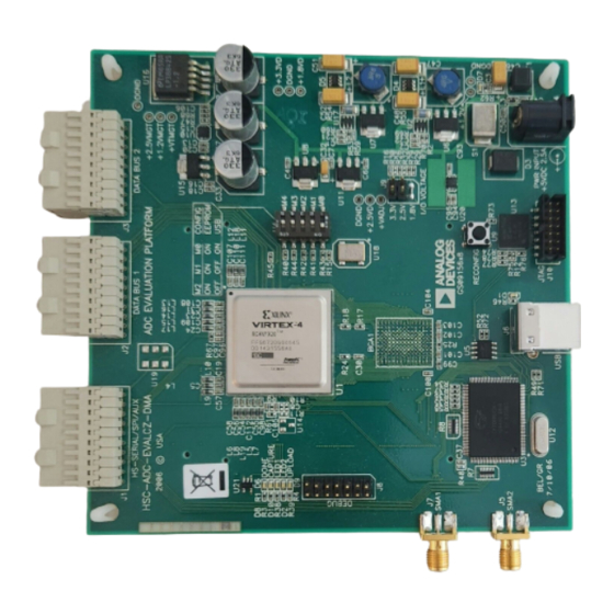
Page 6: Hsc-Adc-Evalc Adc Capture Board Features
HSC-ADC-EVALC HSC-ADC-EVALC ADC CAPTURE BOARD FEATURES GENERAL PURPOSE I/O, USB/SPI CONTROL DATA BUS 1 DATA BUS 2 FPGA LOAD SELECT XILINX VIRTEX-4 FPGA DEBUG ON BOARD PINS POWER SUPPLY 100MHz OSCILLATOR EXTERNAL SYNC I/O FPGA I/O VOLTAGE MODE FPGA CONFIG PROM CYPRESS USB USB CONNECTOR... -
Page 7: Hsc-Adc-Evalc Supported Adc Evaluation Boards
HSC-ADC-EVALC Figure 4. HSC-ADC-EVALC Components (Bottom View) HSC-ADC-EVALC SUPPORTED ADC EVALUATION BOARDS Refer to the Analog Devices ADC capture board product page at www.analog.com/FIFO for a list of HSC-ADC-EVALC-compatible ADC evaluation boards. Some legacy ADC boards may require interposer cards to facilitate proper pin mapping to the ADC capture board. If needed, the interposer part number is noted in the compatibility table at www.analog.com/FIFO... -
Page 8: Theory Of Operation
These functions are not supported beyond the The parallel data input pins of the FPGA, which interface to the scope of this data sheet and the Analog Devices supplied data- converter, are configurable. They can operate with 1.8 V, 2.5 V, capture FPGA routines at this time. -
Page 9: Evaluation Board Schematics And Artwork
HSC-ADC-EVALC EVALUATION BOARD SCHEMATICS AND ARTWORK HSC-ADC-EVALC SCHEMATICS TYCO AND DSP EZ–KIT CONNECTOR TO FPGA XC4VFX20-10FFG672C XC4VFX20-10FFG672C XC4VFX20-10FFG672C XC4VFX20-10FFG672C 51.1Ω 100Ω 100Ω Figure 5. Rev. 0 | Page 9 of 32... - Page 10 HSC-ADC-EVALC SRAM ADDRESS AND CONTROL 3.74KΩ 249Ω 3.74KΩ 3.74KΩ 249Ω FPGA CONTROLS NC7SZ05M5X 100Ω 3.74KΩ 3.74KΩ 3.74KΩ 3.74KΩ 3.74KΩ XC4VFX20-10FFG672C Figure 6. Rev. 0 | Page 10 of 32...
- Page 11 HSC-ADC-EVALC FPGA TO SRAM DATA XC4VFX20-10FFG672C XC4VFX20-10FFG672C Figure 7. Rev. 0 | Page 11 of 32...
- Page 12 HSC-ADC-EVALC AD19 TO BE USED WITH HIGHER DENSITY SRAM DEVICES Figure 8. Rev. 0 | Page 12 of 32...
- Page 13 HSC-ADC-EVALC SRAM AND FPGA POWER 499Ω 499Ω 499Ω 499Ω XC4VFX20-10FFG672C XC4VFX20-10FFG672C Figure 9. Rev. 0 | Page 13 of 32...
- Page 14 HSC-ADC-EVALC SRAM A BYPASS CAP REFCLK Oscillator for IDELAYCTRL 24Ω SRAM B BYPASS CAP FPGA BYPASS CAP Figure 10. Rev. 0 | Page 14 of 32...
- Page 15 HSC-ADC-EVALC UNUSED ROCKET I/0 CONNECTIONS XC4VFX20-10FFG672C XC4VFX20-10FFG672C DEBUG PINS Figure 11. Rev. 0 | Page 15 of 32...
- Page 16 HSC-ADC-EVALC ROCKET I/0 CONNECTIONS Figure 12. Rev. 0 | Page 16 of 32...
- Page 17 HSC-ADC-EVALC USB CONNECTIONS 3.74Ω 3.74Ω 100KΩ SDI & SDO DIRECTIONS ARE WITH RESPECT TO THE DEVICE UNDER CONTROL. Figure 13. Rev. 0 | Page 17 of 32...
- Page 18 HSC-ADC-EVALC USB CONNECTIONS (CONTINUED) 499Ω 3.74KΩ 3.74KΩ XC4VFX20-10FFG672C XC4VFX20-10FFG672C Figure 14. Rev. 0 | Page 18 of 32...
- Page 19 HSC-ADC-EVALC EZ–KIT EXPANSION INTERFACE – FOR DSPs Figure 15. Rev. 0 | Page 19 of 32...
- Page 20 HSC-ADC-EVALC 06676-016 Figure 16. Rev. 0 | Page 20 of 32...
- Page 21 HSC-ADC-EVALC CONFIGURATION EEPROM 100Ω 100Ω ZERO 3.74KΩ 3.74KΩ JTAG CONNECTOR EEPROM HARDWARE RECONFIGURATION PUSHBUTTON 3.74KΩ Figure 17. Rev. 0 | Page 21 of 32...
- Page 22 HSC-ADC-EVALC 06676-018 REMOVE Figure 18. Rev. 0 | Page 22 of 32...
-
Page 23: Pcb Layout
HSC-ADC-EVALC PCB LAYOUT GENERAL PURPOSE I/O, USB/SPI CONTROL DATA BUS 1 DATA BUS 2 XILINX VIRTEX-4 FPGA LOAD FPGA SELECT ON BOARD DEBUG POWER SUPPLY PINS 100MHz OSCILLATOR FPGA I/O VOLTAGE MODE EXTERNAL SYNC I/O CYPRESS USB CONTROLLER FPGA CONFIG PROM USB CONNECTOR FPGA JTAG... -
Page 24: I/O Connector-J1, J2, And J3 Pin Mapping
HSC-ADC-EVALC I/O CONNECTOR—J1, J2, AND J3 PIN MAPPING 06676-021 Figure 21. J2 and J3 Pin Mapping Rev. 0 | Page 24 of 32... - Page 25 HSC-ADC-EVALC MGTCLK1– SD1– SD2– SD3– SD4– SD5– SD6– SD7– SD8– MGTCLK2– HIGH SPEED SERIAL REFERENCE CLK MGTCLK1+ SD1+ SD2+ SD3+ SD4+ SD5+ SD6+ SD7+ SD8+ MGTCLK2+ HIGH SPEED SERIAL DATA INPUTS I/O_1 I/O_3 I/O_5 I/O_7 SCLK USB_1 USB_2 USB_4 FUTURE HIGH SPEED I/O_2 I/O_4 I/O_6...
- Page 26 HSC-ADC-EVALC Table 3. HSC-ADC-EVALC J1 I/O Connections to FPGA (U1) Table 4. HSC-ADC-EVALC J2 I/O Connections to FPGA (U1) Connector J1 Connector J2 (HS-Serial, SPI, AUX) Schematic Net Name FPGA Pin (DATA BUS 1) Schematic Net Name FPGA Pin USB_5 none DCLKB2+ USB_4...
- Page 27 HSC-ADC-EVALC Table 5. HSC-ADC-EVALC J3 I/O Connections to FPGA (U1) Connector J3 (DATA BUS 2) Schematic Net Name FPGA Pin DCLKA2+ DCLKA2− D0A+ D0A− D1A+ D1A− D2A+ D2A− D3A+ D3A− D4A+ D4A− D5A+ D5A− D6A+ D6A− D7A+ D7A− D8A+ D8A− D9A+ D9A−...
-
Page 28: Ordering Information
HSC-ADC-EVALC ORDERING INFORMATION BILL OF MATERIALS (RoHS COMPLIANT) Table 6. Reference Designator Description Manufacturer Part Number PCB, ADC evaluation platform MOOG/PCSM GS09156x8 BGA1, BGA2 IC, 18-bit DDRII SRAM 2-word burst PD44164362F5-EQ1 operation (MOS integrated circuit), do not install C1, C2 Panasonic/ECG ECJ-0EB1H471K Capacitor, 470 pF, 50 V ceramic... - Page 29 DLW5AH/DLW5BS series (2014/2020 Size) Virtex-4 FPGA Xilinx XC4VFX20-10FFG672C U10, U20 Voltage regulator, high accuracy, low IQ, Analog Devices ADP3334ACPZ-REEL7 adjustable U11, U15 Voltage regulator, high accuracy Analog Devices ADP3339AKCZ-2.5R7 ultralow IQ, 1.5 A Crystal oscillator, 24 Mhz, 12 pF, SMD ECS-240-12-4X 1.8 V, 8 Mb, platform flash-in system...
-
Page 30: Ordering Guide
Part Number U6, U7 IC, P-channel enhancement mode field Fairchild Semiconductor NDT456P effect transistor Voltage regulator, high accuracy Analog Devices ADP3339AKCZ-3.3 ultralow IQ, 1.5 A Switch, 6 mm light touch SW, N.O. Alps SKHHAKA010 H1, H2, H3, H4 Circuit board support on base Richco, Inc. - Page 31 HSC-ADC-EVALC NOTES Rev. 0 | Page 31 of 32...
- Page 32 HSC-ADC-EVALC NOTES ©2007 Analog Devices, Inc. All rights reserved. Trademarks and registered trademarks are the property of their respective owners. EB06676-0-4/07(0) Rev. 0 | Page 32 of 32...
Need help?
Do you have a question about the HSC-ADC-EVALC and is the answer not in the manual?
Questions and answers