
Related Manuals for ADLINK Technology SMARC LEC-RB5 N


Summary of Contents for ADLINK Technology SMARC LEC-RB5 N
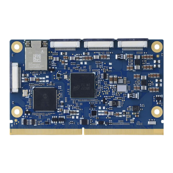
- Page 1 LEC-iMX8MM User’s Guide SMARC R2.1 LEC-RB5(N) User’s Guide Revision: Rev. 0.1 Date: 2023-09-21 Part Number: 50M-72515-1000 Page 1 Copyright © 2023 ADLINK Technology, Inc.
-
Page 2: Revision History
Revision History Revision Description Date Author Preliminary release 2023-09-21 copyright © 2023 ADLINK Technology Inc. -
Page 3: Preface
Product names mentioned herein are used for identification purposes only and may be trademarks / registered trademarks of respective companies. Copyright © 2023 ADLINK Technology Incorporated This document contains proprietary information protected by copyright. All rights are reserved. No part of this manual may be reproduced by any mechanical, electronic, or other means in any form without prior written permission of the manufacturer. - Page 4 Caution: This information indicates the possibility of minor physical injury, component damage, data loss, and/or program corruption. Warning: This information warns of possible serious physical injury, component damage, data loss, and/or program corruption. Page 4 copyright © 2023 ADLINK Technology Inc.
- Page 5 ADLINK Technology GmbH Hans-Thoma-Strasse 11, D-68163 Mannheim, Germany Tel: +49-621-43214-0 Fax: +49-621 43214-30 Email: emea@adlinktech.com Please visit the Contact page at www.adlinktech.com for information on how to contact the ADLINK regional office nearest you. Page 5 copyright © 2023 ADLINK Technology Inc.
- Page 6 Product names mentioned herein are used for identification purposes only and may be trademarks and/or registered trademarks of their respective companies. © Copyright 2017 ADLINK Technology, Incorporated This document contains proprietary information protected by copyright. All rights are reserved. No part of this manual may be reproduced by any mechanical, electronic, or other means in any form without prior written permission of the manufacturer.
-
Page 7: Table Of Contents
Signal Terminology Descriptions ........................................................... 23 Signal Description by function ..........................................................24 4.3.1 Primary Display Interface ..........................................................24 Secondary Display Interface ............................................................. 26 4.4.1 HDMI Mode ............................................................... 26 4.4.2 MIPI Camera Support ............................................................. 27 Page 7 copyright © 2023 ADLINK Technology Inc. - Page 8 Early Access ..................................................................46 Yocto....................................................................46 Ubuntu ..................................................................... 46 6. Mechanical ..............................................................47 Module Dimensions ..............................................................47 7. Thermal Solutions ............................................................ 48 Heatspreader – HTS ..............................................................48 Heatsink – THS ................................................................49 Page 8 copyright © 2023 ADLINK Technology Inc.
-
Page 9: List Of Figures
Figure 1 – Module functional block diagram ..................................................18 Figure 2 – Module top/botom side pin numbering ................................................. 19 Figure 3 – Module dimensions ........................................................47 Figure 4 – Heatspreader HTS ........................................................48 Figure 5 – Heatsink THS ..........................................................49 Page 9 copyright © 2023 ADLINK Technology Inc. -
Page 10: Introduction
The modular approach allows scalability, faster time to market and upgradability while still maintaining low costs, low power, and small physical size. SMARC module and carrier specifications are available online at: https://www.sget.org/standards/smarc.html Page 10 copyright © 2023 ADLINK Technology Inc. -
Page 11: Specifications
• Four-channel PoP high speed memory LPDDR5 SDRAM @ 2750MHz, up to 8GB L2 Cache System L2 cache (ECC) Gold core 256 KB • Gold Prime core 512 KB • Silver core 128 KB • Security Qualcomm Secure Processing Unit Page 11 copyright © 2023 ADLINK Technology Inc. -
Page 12: Video
Maximum resolution 1K p60 with 24-bit RGB HDMI • HDMI interface is obtained from DSI0/1 over a DSI2HDMI chip (need 8 lanes) • HDMI 2.0B complaint • Supports a maximum display resolution of 1K p60 Page 12 copyright © 2023 ADLINK Technology Inc. -
Page 13: Camera
10/100/1000 Ethernet Controller over USB 3.1 Supports 10/100/1000-Mbps data transfer rates, both full-duplex and half-duplex Secondary LAN 10/100/1000 Ethernet Controller over USB 3.1 Supports 10/100/1000-Mbps data transfer rates, both full-duplex and half-duplex Page 13 copyright © 2023 ADLINK Technology Inc. -
Page 14: Wi-Fi / Bluetooth
Optional CAN0 Supports CAN2.0B only or mixed CAN2.0B and CAN FD mode, data bit rate up to 8 Mbps (Optional over SPI1) 2x SPI I2S / Sound Wire 1x I2S with audio resolution from 16-bits to 32-bits and sample rate up to 192KHz (see Audio Codec support) Page 14 copyright © 2023 ADLINK Technology Inc. -
Page 15: System Storage
14x GPIO with interrupt, one GPIO with PWM 2.8 System Storage SDIO 1x SDIO (4-bit) compatible with SD3.0, MMC ver. 4.51 to edge connector Storage Up to 256 GB on-module UFS 2.9 Board Controller BMC lite for power sequence Page 15 copyright © 2023 ADLINK Technology Inc. -
Page 16: Debug Header Db30
Rugged Operating Temperature: -20 to 70°C industrial grade BOM (memory, eMMC, USB hub, SoC) Humidity: 5-90% RH operating, non-condensing 5-95% RH storage (and operating with conformal coating). EMI: EN55022 Class B inside an enclosure Page 16 copyright © 2023 ADLINK Technology Inc. - Page 17 Capable of supporting Random Vibration: MIL-STD-202F, Method 214A, Table 214-I, Condition D. If HALT testing shows equal or better performance, a separate vibration test report is not necessary. MTBF: 300,000 hrs (at 40°C), 100,000 hrs (at 70°C), Page 17 copyright © 2023 ADLINK Technology Inc.
-
Page 18: Block Diagram
UART2 / 4W SD/SDIO SDIO_3.0 BMC_Lite SPI 0 SPI_0 SPI_3 SPI 1 CAN FD SPI_1 MCP2518FDT GPIO GPIO x14 I2S_SND i2S / SoundWire I2C x3 Figure 1 – Module functional block diagram Page 18 copyright © 2023 ADLINK Technology Inc. -
Page 19: Pinout And Signal Descriptions
Not all signals are available in each design, for specific product specs check the detailed tables in this document. Top Side Bottom Side P156 S156 Figure 2 – Module top/botom side pin numbering Page 19 copyright © 2023 ADLINK Technology Inc. - Page 20 USB0- USB3_SSTX+ GBE0_CTREF PCIE_D_TX+ / SERDES_1_TX+ USB0_EN_OC# USB3_SSTX- GBE0_MDI0- PCIE_D_TX- / SERDES_1_TX- USB0_VBUS_DET GBE0_MDI0+ GBE1_LINK_ACT# USB0_OTG_ID USB3_SSRX+ (build option) SPI0_CS1# PCIE_D_RX+ / SERDES_1_RX+ USB1+ USB3_SSRX- PCIE_D_RX- / SERDES_1_RX- USB1- SDIO_WP USB1_EN_OC# USB3+ Page 20 copyright © 2023 ADLINK Technology Inc.
- Page 21 LVDS0_1- / eDP0_TX1- / DSI0_D1- HDMI_D1+ / DP0_LANE1+ P129 SER0_TX S130 HDMI_D1- / DP1_LANE1- DP0_LANE1- P130 SER0_RX S131 LVDS0_2+/eDP0_TX2+/ DSI0_D2+ DP0_HPD P131 SER0_RTS# S132 LVDS0_2- / eDP0_TX2- / DSI0_D2- HDMI_D0+ / DP0_LANE2+ P132 SER0_CTS# S133 LCD0_VDD_EN Page 21 copyright © 2023 ADLINK Technology Inc.
- Page 22 P143 CAN0_TX S144 eDP0_HPD / DSI0_TE P156 VDD_IN S157 TEST# P144 CAN0_RX S145 WDT_TIME_OUT# S158 P145 CAN1_TX S146 PCIE_WAKE# Note: Above is the complete SMARC function set, not all signals are available Page 22 copyright © 2023 ADLINK Technology Inc.
-
Page 23: Signal Terminology Descriptions
Module is in its lowest power state Runtime Module is full on. CARRIER_PWRON is high and CARRIER_SBY# is NOT active (i.e. both signals are high) Standby Module is in standby state or higher Page 23 copyright © 2023 ADLINK Technology Inc. -
Page 24: Signal Description By Function
LCD1_VDD_EN LCD1_VDD_EN S127 LCD0_BKLT_EN LCD0_BKLT_EN LCD0_BKLT_EN S107 LCD1_BKLT_EN LCD1_BKLT_EN LCD1_BKLT_EN S141 LCD0_BKLT_PWM LCD0_BKLT_PWM LCD0_BKLT_PWM S122 LCD1_BKLT_PWM LCD1_BKLT_PWM LCD1_BKLT_PWM S144 DSI0_TE eDP0_HPD S113 DSI1_TE eDP1_HPD S139 I2C_LCD_CK I2C_LCD_CK I2C_LCD_CK S140 I2C_LCD_DAT I2C_LCD_DAT I2C_LCD_DAT Page 24 copyright © 2023 ADLINK Technology Inc. - Page 25 DDC data line used for flat panel I/O OD 1.8V Runtime PU 2k2 detection and control CMOS I2C_LCD_CK S139 DDC clock line used for flat panel O OD 1.8V Runtime PU 2k2 detection and control CMOS Page 25 copyright © 2023 ADLINK Technology Inc.
-
Page 26: Secondary Display Interface
HDMI_HPD P104 HDMI Hot plug active high detection 1.8V Runtime PD 1M Important: Module shall tolerate high level in stand-by signal that serves as an interrupt CMOS mode request Page 26 copyright © 2023 ADLINK Technology Inc. -
Page 27: Mipi Camera Support
Shared with GPIO0 GPIO0 output. CAM0_RST# / P110 Camera 0 reset, active low output O CMOS 1.8V Runtime PU 470k Shared with GPIO2 GPIO2 CAM_MCK Master clock output O CMOS 1.8V Runtime Page 27 copyright © 2023 ADLINK Technology Inc. - Page 28 Master clock output O CMOS 1.8V Runtime Note: LEC-RB5 has support for up to 6 cameras. CSI 0,1 go to the carrier while CSI 2,3,4,5 are located on feature connectors of the module. Page 28 copyright © 2023 ADLINK Technology Inc.
-
Page 29: Csi Feature Connectors
MIPI Data Lane 2 Positive Ground CAM_D3_N MIPI Data Lane 3 Negative CAM_D3_P MIPI Data Lane 3 Positive Ground CAM_IO0 Power Enable CAM_IO1 LED Indicator Ground CAM_SCL I2C SCL CAM_SDA I2C SDA CAM_3V3 3.3V Power Output Page 29 copyright © 2023 ADLINK Technology Inc. -
Page 30: Audio Interfaces
Module Input if CPU acts in Slave Mode AUDIO_MCK Master clock output to I2S 1.8V Runtime Shared with I2S2 codec(s) CMOS Note: I2S1 signalling has been removed during update to SMARC 2.0 specification Page 30 copyright © 2023 ADLINK Technology Inc. -
Page 31: I2S2 Mode
I2S2 Digital audio clock 1.8V Runtime Module Output if CPU acts in Master Mode CMOS Module Input if CPU acts in Slave Mode AUDIO_MCK Master clock output to I2S 1.8V Runtime codec(s) CMOS Page 31 copyright © 2023 ADLINK Technology Inc. -
Page 32: Usb Ports
USB over-current sense for port 2 I/O OD 3.3V Standby PU 10k Pulled low by Module OD driver to disable USB2 power. note 1 CMOS Pulled low by Carrier OD driver to indicate over-current situation. Page 32 copyright © 2023 ADLINK Technology Inc. - Page 33 1. 3.3V or switched 3.3V: if a USB channel is not used, then USB[0:5]_EN_OC# pull-up rails may be held at GND to prevent current leakage. 2. USB0 is directly connected to the SoC and offers OTG, while others use a shared bandwidth through a USB 2.0/3.1HUB. Page 33 copyright © 2023 ADLINK Technology Inc.
-
Page 34: Pcie Ports
PCIe Port B reset output 3.3V Runtime CMOS PCIE_B_CKREQ# PCIe Port B clock request I OD 3.3V Runtime Can be used for power saving mode on PCIe - CMOS Pulled up or terminated on Module Page 34 copyright © 2023 ADLINK Technology Inc. - Page 35 I LVDS Runtime Series AC coupled off module PCIE_C_RX- PCIE PCIE_C_REFCK+ Differential PCIe Link C reference clock O LVDS Runtime PCIE_C_REFCK- output PCIE PCIE_C_RST# PCIe Port C reset output 3.3V Runtime CMOS Page 35 copyright © 2023 ADLINK Technology Inc.
-
Page 36: Dual Lan Ports
IEEE 1588 Trigger Signal. For hardware implementation 3.3V Standby of PTP (precision time protocol) CMOS Note: LAN ports are derived from USB. There are no native LAN port in the QRB5165 SoC Page 36 copyright © 2023 ADLINK Technology Inc. -
Page 37: Gbe1
IEEE 1588 Trigger Signal. For hardware implementation 3.3V Standby of PTP (precision time protocol) CMOS Note: LAN ports are derived from USB. There are no native LAN port in the QRB5165 SoC Page 37 copyright © 2023 ADLINK Technology Inc. -
Page 38: Sdio Card (4-Bit)
SDIO_PWR_EN SDIO Power Enable. This signal is used to 3.3V Runtime should be driven low in STB Mode by the enable the power being supplied to a SD/MMC card CMOS module device. Page 38 copyright © 2023 ADLINK Technology Inc. -
Page 39: Spi Interfaces
MISO can also be used as ESPI_IO_1 SPI1_DO SPI1 Master output / Slave input O CMOS 1.8V Standby also referred to as MOSI can also be used as ESPI_IO_0 Page 39 copyright © 2023 ADLINK Technology Inc. -
Page 40: Gpio
General purpose I/O pin 13 1.8V Runtime PU 470k CMOS Note: In-SoC Pull-Ups allowed. These can be ≤ 10k. Max 2.2k PD should be implemented on Carrier if a low level needs to be ensured. Page 40 copyright © 2023 ADLINK Technology Inc. -
Page 41: Can Bus
Driven by OD on Carrier WDT_TIME_OUT# S145 Watch-Dog-Timer Output, low active. 1.8V Runtime CMOS PWM_OUT P113 Pulse Width Modulation (PWM) 1.8V Runtime PU 470k GPIO5 is the default pin configuration / GPIO5 output CMOS Page 41 copyright © 2023 ADLINK Technology Inc. -
Page 42: Power And System Management
1.8V to 5V Standby PU 10k Driven by OD on Carrier. float the line in in-active state. Active low, level CMOS Pulled up on module. sensitive. Should be debounced on the Module. Page 42 copyright © 2023 ADLINK Technology Inc. - Page 43 On x86 systems these serve as SMB CMOS Sleep CLK. Pulled up on module. SMB_ALERT_1V8# SMBus Alert# (interrupt) signal I OD 1.8V to 5V Standby/ PU 2k2 only used on x86 design CMOS Sleep Page 43 copyright © 2023 ADLINK Technology Inc.
-
Page 44: Boot Select
SOC native Force Recovery mode – such as over a Serial Port. For x86 systems this signal may be used to load BIOS defaults. Pulled up on Module. Driven by OD part on Carrier. Page 44 copyright © 2023 ADLINK Technology Inc. -
Page 45: Power
P Not defined within Signal [2 to 3.25] / 3.25V power – 3.0V nominal. May be Terminology Descriptions. sourced from a Carrier based Should we define a specific Lithium cell or Super Cap. rail? Page 45 copyright © 2023 ADLINK Technology Inc. -
Page 46: Software Support
5. Software Support 5.1 Early Access this product will only support Ubuntu at launch ROS2 will be implemented in Ubuntu ALL software use the standard QC release 5.2 Yocto 5.3 Ubuntu Standard OS Page 46 copyright © 2023 ADLINK Technology Inc. -
Page 47: Mechanical
LEC-RB5 User’s Guide SGET SMARC R2.1.1 6. Mechanical 6.1 Module Dimensions SMARC Short Size: 82x 50mm Figure 3 – Module dimensions Page 47 copyright © 2023 ADLINK Technology Inc. -
Page 48: Thermal Solutions
LEC-RB5 User’s Guide SGET SMARC R2.1.1 7. Thermal Solutions 7.1 Heatspreader – HTS Sustainable temperature range with high performance LAB copper heatsink with high airflow = -40~85°C ambient Figure 4 – Heatspreader HTS Page 48 copyright © 2023 ADLINK Technology Inc. -
Page 49: Heatsink - Ths
LEC-RB5 User’s Guide SGET SMARC R2.1.1 7.2 Heatsink – THS Sustainable temperature range with moderate airflow = 0~60°C ambient Figure 5 – Heatsink THS Page 49 copyright © 2023 ADLINK Technology Inc.
Need help?
Do you have a question about the SMARC LEC-RB5 N and is the answer not in the manual?
Questions and answers