Table of Contents
Advertisement
Quick Links
Features
■
Very high speed: 45 ns
■
Temperature ranges
❐
Industrial: –40°C to +85°C
❐
Automotive-A: –40°C to +85°C
❐
Automotive-E: –40°C to +125°C
■
Wide voltage range: 2.20V to 3.60V
■
Pin compatible with CY62147DV30
■
Ultra low standby power
Typical standby current: 1 μA
❐
Maximum standby current: 7 μA (Industrial)
❐
■
Ultra low active power
❐
Typical active current: 2 mA at f = 1 MHz
■
Easy memory expansion with CE
■
Automatic power down when deselected
■
CMOS for optimum speed and power
■
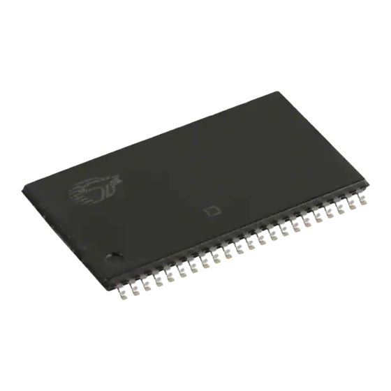
Available in Pb-free 48-ball VFBGA (single/dual CE option) and
44-pin TSOPII packages
■
Byte power down feature
Functional Description
The CY62147EV30 is a high performance CMOS static RAM
organized as 256K words by 16 bits. This device features
advanced circuit design to provide ultra low active current. It is
Logic Block Diagram
POWER DOWN
Note
1. BGA packaged device is offered in single CE and dual CE options. In this data sheet, for a dual CE device, CE refers to the internal logical combination of CE
CE
such that when CE
is LOW and CE
2
1
Cypress Semiconductor Corporation
Document #: 38-05440 Rev. *G
[1]
and OE features
A
10
A
9
A
8
A
7
A
6
A
5
A
4
A
3
A
2
A
1
A
0
CE
BHE
CIRCUIT
BLE
is HIGH, CE is LOW. For all other cases CE is HIGH.
2
•
198 Champion Court
4-Mbit (256K x 16) Static RAM
ideal for providing More Battery Life™ (MoBL
cations such as cellular telephones. The device also has an
automatic power down feature that significantly reduces power
consumption when addresses are not toggling. Placing the
device into standby mode reduces power consumption by more
than 99% when deselected (CE HIGH or both BLE and BHE are
HIGH). The input and output pins (IO
in a high impedance state when:
■
Deselected (CE HIGH)
■
Outputs are disabled (OE HIGH)
■
Both Byte High Enable and Byte Low Enable are disabled
(BHE, BLE HIGH)
■
Write operation is active (CE LOW and WE LOW)
To write to the device, take Chip Enable (CE) and Write Enable
(WE) inputs LOW. If Byte Low Enable (BLE) is LOW, then data
from IO pins (IO
through IO
0
specified on the address pins (A
Enable (BHE) is LOW, then data from IO pins (IO
is written into the location specified on the address pins (A
through A
).
17
To read from the device, take Chip Enable (CE) and Output
Enable (OE) LOW while forcing the Write Enable (WE) HIGH. If
Byte Low Enable (BLE) is LOW, then data from the memory
location specified by the address pins appear on IO
Byte High Enable (BHE) is LOW, then data from memory
appears on IO
to IO
8
complete description of read and write modes.
For best practice recommendations, refer to the Cypress
application note
AN1064, SRAM System
DATA IN DRIVERS
256K x 16
RAM Array
COLUMN DECODER
,
•
San Jose
CY62147EV30 MoBL
®
) in portable appli-
through IO
0
15
) is written into the location
7
through A
). If Byte High
0
17
through IO
8
. See the
Truth Table
on page 9 for a
15
Guidelines.
IO
–IO
0
7
IO
–IO
8
15
BHE
WE
[1]
CE
OE
BLE
CA 95134-1709
•
408-943-2600
Revised March 31, 2009
®
) are placed
)
15
0
to IO
. If
0
7
and
1
[+] Feedback
Advertisement
Table of Contents

Related Manuals for Cypress Semiconductor Perform CY62147EV30


Summary of Contents for Cypress Semiconductor Perform CY62147EV30
-
Page 1: Functional Description
Features ■ Very high speed: 45 ns ■ Temperature ranges ❐ Industrial: –40°C to +85°C ❐ Automotive-A: –40°C to +85°C ❐ Automotive-E: –40°C to +125°C ■ Wide voltage range: 2.20V to 3.60V ■ Pin compatible with CY62147DV30 ■ Ultra low standby power Typical standby current: 1 μA ❐... -
Page 2: Product Portfolio
Product Portfolio Product Range CY62147EV30LL Ind’l/Auto-A Auto-E Pin Configuration Figure 1. 48-Ball VFBGA (Single Chip Enable) Notes 2. Typical values are included for reference only and are not guaranteed or tested. Typical values are measured at V 3. NC pins are not connected on the die. 4. -
Page 3: Maximum Ratings
Maximum Ratings Exceeding the maximum ratings may impair the useful life of the device. User guidelines are not tested. Storage Temperature ... –65°C to + 150°C Ambient Temperature with Power Applied ... –55°C to + 125°C Supply Voltage to Ground Potential ... -
Page 4: Thermal Resistance
Thermal Resistance Parameter Description Θ Thermal Resistance (Junction to Ambient) Θ Thermal Resistance (Junction to Case) OUTPUT 30 pF INCLUDING JIG AND SCOPE Equivalent to: THEVENIN EQUIVALENT Parameters Data Retention Characteristics Over the Operating Range Parameter Description for Data Retention Data Retention Current CCDR Chip Deselect to Data Retention Time... -
Page 5: Switching Characteristics
Switching Characteristics [12, 13] Over the Operating Range Parameter Description Read Cycle Read Cycle Time Address to Data Valid Data Hold from Address Change CE LOW to Data Valid OE LOW to Data Valid OE LOW to LOW Z LZOE OE HIGH to High Z HZOE CE LOW to Low Z... -
Page 6: Switching Waveforms
Switching Waveforms Figure 6. Read Cycle No. 1 (Address Transition Controlled) ADDRESS PREVIOUS DATA VALID DATA OUT Figure 7. Read Cycle No. 2 (OE Controlled) ADDRESS LZOE BHE/BLE LZBE HIGH IMPEDANCE DATA OUT LZCE SUPPLY CURRENT Notes 17. The device is continuously selected. OE, CE = V 18. - Page 7 Switching Waveforms (continued) Figure 8. Write Cycle No. 1 (WE Controlled) ADDRESS BHE/BLE NOTE 22 DATA IO HZOE Figure 9. Write Cycle No. 2 (CE Controlled) ADDRESS BHE/BLE DATA IO NOTE 22 HZOE Document #: 38-05440 Rev. *G [1, 16, 20, 21] DATA [1, 16, 20, 21] DATA...
- Page 8 Switching Waveforms (continued) Figure 10. Write Cycle No. 3 (WE Controlled, OE LOW) ADDRESS BHE/BLE DATA IO NOTE 22 HZWE Figure 11. Write Cycle No. 4 (BHE/BLE Controlled, OE LOW) ADDRESS BHE/BLE NOTE 22 DATA IO Notes 20. Data I/O is high impedance if OE = V 21.
-
Page 9: Truth Table
Truth Table Ordering Information Speed Ordering Code (ns) CY62147EV30LL-45BVI CY62147EV30LL-45BVXI CY62147EV30LL-45B2XI CY62147EV30LL-45ZSXI CY62147EV30LL-45BVXA CY62147EV30LL-45ZSXA CY62147EV30LL-55ZSXE Contact your local Cypress sales representative for availability of these parts. Notes 23. This BGA package is offered with single chip enable. 24. This BGA package is offered with dual chip enable. Document #: 38-05440 Rev. -
Page 10: Package Diagrams
Package Diagrams Figure 12. 48-Ball VFBGA (6 x 8 x 1 mm), 51-85150 TOP VIEW A1 CORNER 6.00±0.10 SEATING PLANE Document #: 38-05440 Rev. *G CY62147EV30 MoBL BOTTOM VIEW A1 CORNER Ø0.05 M C Ø0.25 M C A B Ø0.30±0.05(48X) 1.875 0.75 3.75... - Page 11 ® CY62147EV30 MoBL Package Diagrams (continued) Figure 13. 44-Pin TSOP II, 51-85087 51-85087-*A Document #: 38-05440 Rev. *G Page 11 of 13 [+] Feedback...
- Page 12 Document History Page Document Title: CY62147EV30 MoBL Document Number: 38-05440 Orig. of Submission Rev. ECN No. Change 201861 01/13/04 247009 See ECN 414807 See ECN 464503 See ECN 925501 See ECN 1045701 See ECN 2577505 VKN/PYRS 10/03/08 2681901 VKN/PYRS 04/01/09 Document #: 38-05440 Rev.
- Page 13 Sales, Solutions, and Legal Information Worldwide Sales and Design Support Cypress maintains a worldwide network of offices, solution centers, manufacturer’s representatives, and distributors. To find the office closest to you, visit us at cypress.com/sales. Products PSoC Clocks & Buffers Wireless wireless.cypress.com Memories memory.cypress.com...
Need help?
Do you have a question about the Perform CY62147EV30 and is the answer not in the manual?
Questions and answers