Table of Contents
Advertisement
Quick Links
Features
• Very high speed: 45 ns
• Wide voltage range: 4.5V–5.5V
• Ultra-low standby power
—Typical Standby current: 2 µA
—Maximum Standby current: 8 µA (Industrial)
• Ultra-low active power
— Typical active current: 1.8 mA @ f = 1 MHz
• Ultra-low standby power
• Easy memory expansion with CE
• Automatic power-down when deselected
• CMOS for optimum speed/power
• Available in Pb-free 44-pin TSOP II and 48-ball VFBGA
package
Functional Description
The CY62157E is a high-performance CMOS static RAM
organized as 512K words by 16 bits. This device features
advanced circuit design to provide ultra-low active current.
This is ideal for providing More Battery Life™ (MoBL
portable applications such as cellular telephones. The device
Logic Block Diagram
Note:
1. For best practice recommendations, please refer to the Cypress application note "System Design Guidelines" on http://www.cypress.com.
Cypress Semiconductor Corporation
Document #: 38-05695 Rev. *C
, CE
and OE features
1
2
[1]
®
) in
DATA IN DRIVERS
A
10
A
9
A
8
A
7
A
6
512K x 16
A
5
RAM Array
A
4
A
3
A
2
A
1
A
0
COLUMN DECODER
POWER-DOWN
CIRCUIT
•
198 Champion Court
8-Mbit (512K x 16) Static RAM
also has an automatic power-down feature that significantly
reduces power consumption when addresses are not toggling.
The device can also be put into standby mode when
deselected (CE
HIGH or CE
1
2
HIGH). The input/output pins (IO
a high-impedance state when: deselected (CE
LOW), outputs are disabled (OE HIGH), both Byte High
Enable and Byte Low Enable are disabled (BHE, BLE HIGH),
or during a write operation (CE
LOW).
Writing to the device is accomplished by taking Chip Enable
(CE
LOW and CE
HIGH) and Write Enable (WE) input LOW.
1
2
If Byte Low Enable (BLE) is LOW, then data from IO pins (IO
through IO
), is written into the location specified on the
7
address pins (A
through A
0
18
LOW, then data from IO pins (IO
the location specified on the address pins (A
Reading from the device is accomplished by taking Chip
Enable (CE
LOW and CE
HIGH) and Output Enable (OE)
1
2
LOW while forcing the Write Enable (WE) HIGH. If Byte Low
Enable (BLE) is LOW, then data from the memory location
specified by the address pins will appear on IO
High Enable (BHE) is LOW, then data from memory will appear
on IO
to IO
. See the truth table at the back of this data sheet
8
15
for a complete description of read and write modes.
IO
–IO
0
IO
–IO
8
BHE
WE
OE
BLE
BHE
BLE
,
•
San Jose
CA 95134-1709
CY62157E MoBL
LOW or both BHE and BLE are
through IO
) are placed in
0
15
HIGH or CE
1
LOW, CE
HIGH and WE
1
2
). If Byte High Enable (BHE) is
through IO
) is written into
8
15
through A
).
0
18
to IO
. If Byte
0
7
7
15
CE
2
CE
1
CE
2
CE
1
•
408-943-2600
Revised November 21, 2006
®
2
0
[+] Feedback
Advertisement
Table of Contents

Related Manuals for Cypress Semiconductor MoBL CY62157E


Summary of Contents for Cypress Semiconductor MoBL CY62157E
- Page 1 Features • Very high speed: 45 ns • Wide voltage range: 4.5V–5.5V • Ultra-low standby power —Typical Standby current: 2 µA —Maximum Standby current: 8 µA (Industrial) • Ultra-low active power — Typical active current: 1.8 mA @ f = 1 MHz •...
-
Page 2: Pin Configuration
[2, 3] Pin Configuration TSOP II Top View Product Portfolio Product Range CY62157E-45 Ind’l CY62157E-55 Auto Notes: 2. NC pins are not connected on the die. 3. The 44-pin TSOP II package has only one chip enable (CE) pin. 4. Typical values are included for reference only and are not guaranteed or tested. Typical values are measured at V 5. -
Page 3: Maximum Ratings
Maximum Ratings (Above which the useful life may be impaired. For user guide- lines, not tested.) Storage Temperature ... –65°C to + 150°C Ambient Temperature with Power Applied ... –55°C to + 125°C Supply Voltage to Ground Potential ... –0.5V to 6.0V DC Voltage Applied to Outputs [6, 7] in High Z State... - Page 4 Thermal Resistance Parameter Description Θ Thermal Resistance (Junction to Ambient) Θ Thermal Resistance (Junction to Case) AC Test Loads and Waveforms OUTPUT 30 pF INCLUDING JIG AND SCOPE Parameters Data Retention Characteristics Parameter Description for Data Retention Data Retention Current CCDR Chip Deselect to Data Retention Time...
-
Page 5: Switching Characteristics
Switching Characteristics Over the Operating Range Parameter Description Read Cycle Read Cycle Time Address to Data Valid Data Hold from Address Change LOW and CE HIGH to Data Valid OE LOW to Data Valid [13] OE LOW to LOW Z LZOE [13, 14] OE HIGH to High Z... - Page 6 Switching Waveforms Read Cycle 1 (Address Transition Controlled) ADDRESS PREVIOUS DATA VALID DATA OUT [17, 18] Read Cycle 2 (OE Controlled) ADDRESS BHE/BLE LZBE LZOE HIGH IMPEDANCE DATA OUT LZCE SUPPLY CURRENT Notes: 16. The device is continuously selected. OE, CE 17.
- Page 7 Switching Waveforms (continued) [15, 19, 20, 21] Write Cycle 1 (WE Controlled) ADDRESS BHE/BLE DATA IO See Note 21 HZOE Write Cycle 2 (CE or CE Controlled) ADDRESS BHE/BLE DATA IO See Note 21 HZOE Notes: 19. Data IO is high impedance if OE = V 20.
- Page 8 Switching Waveforms (continued) Write Cycle 3 (WE Controlled, OE LOW) ADDRESS BHE/BLE DATA IO See Note 21 Write Cycle 4 (BHE/BLE Controlled, OE LOW) ADDRESS BHE/BLE DATA IO See Note 21 Document #: 38-05695 Rev. *C [20, 21] VALID DATA HZWE [20, 21] VALID DATA...
-
Page 9: Truth Table
Truth Table Ordering Information Speed (ns) Ordering Code CY62157ELL-45ZSXI 51-85087 CY62157ELL-55ZSXE 51-85087 CY62157ELL-55BVXE 51-85150 Document #: 38-05695 Rev. *C Inputs/Outputs High Z High Z High Z Data Out (IO –IO Data Out (IO –IO High Z (IO –IO High Z (IO –IO Data Out (IO –IO... -
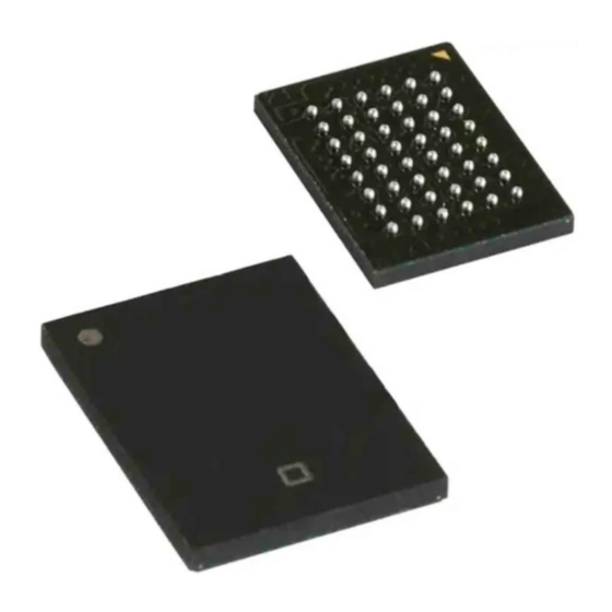
Page 10: Package Diagrams
® CY62157E MoBL Package Diagrams 44-pin TSOP II (51-85087) 51-85087-*A Document #: 38-05695 Rev. *C Page 10 of 12 [+] Feedback... - Page 11 Package Diagrams (continued) TOP VIEW A1 CORNER 6.00±0.10 SEATING PLANE MoBL is a registered trademark, and More Battery Life is a trademark, of Cypress Semiconductor Corporation. All product and company names mentioned in this document are the trademarks of their respective holders. Document #: 38-05695 Rev.
- Page 12 Document History Page ® Document Title: CY62157E MoBL , 8-Mbit (512K x 16) Static RAM Document Number: 38-05695 Orig. of REV. ECN NO. Issue Date Change 291273 See ECN 457689 See ECN 467033 See ECN 569114 See ECN Document #: 38-05695 Rev. *C Description of Change New data sheet Added Automotive Product...
Need help?
Do you have a question about the MoBL CY62157E and is the answer not in the manual?
Questions and answers