Table of Contents
Advertisement
Quick Links
Features
• Very high speed: 45 ns
• Wide voltage range: 2.20V–3.60V
• Pin compatible with CY62146DV30
• Ultra low standby power
— Typical standby current: 1 µA
— Maximum standby current: 7 µA
• Ultra low active power
— Typical active current: 2 mA @ f = 1 MHz
• Easy memory expansion with CE, and OE features
• Automatic power down when deselected
• CMOS for optimum speed and power
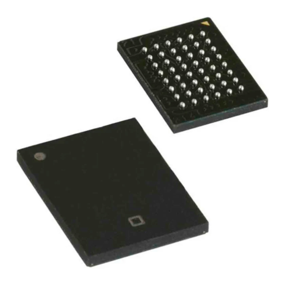
• Available in a Pb-free 48-ball VFBGA and 44-pin TSOP II
packages
Functional Description
The CY62146EV30 is a high performance CMOS static RAM
organized as 256K words by 16 bits. This device features
advanced circuit design to provide ultra low active current.
This is ideal for providing More Battery Life™ (MoBL
portable applications such as cellular telephones. The device
also has an automatic power down feature that significantly
Product Portfolio
Product
Min
CY62146EV30LL
2.2
Notes:
1. For best practice recommendations, please refer to the Cypress application note System Design Guidelines on http://www.cypress.com.
2. Typical values are included for reference only and are not guaranteed or tested. Typical values are measured at V
Cypress Semiconductor Corporation
Document #: 38-05567 Rev. *C
[1]
®
) in
Speed
V
Range (V)
CC
[2]
Typ
Max
3.0
3.6
•
198 Champion Court
4-Mbit (256K x 16) Static RAM
reduces power consumption by 80% when addresses are not
toggling. The device can also be put into standby mode
reducing power consumption by more than 99% when
deselected (CE HIGH). The input and output pins (IO
IO
) are placed in a high impedance state when:
15
• Deselected (CE HIGH)
• Outputs are disabled (OE HIGH)
• Both Byte High Enable and Byte Low Enable are disabled
(BHE, BLE HIGH)
• Write operation is active (CE LOW and WE LOW)
Write to the device by taking Chip Enable (CE) and Write
Enable (WE) inputs LOW. If Byte Low Enable (BLE) is LOW,
then data from IO pins (IO
location specified on the address pins (A
High Enable (BHE) is LOW, then data from IO pins (IO
through IO
) is written into the location specified on the
15
address pins (A
through A
0
Read from the device by taking Chip Enable (CE) and Output
Enable (OE) LOW while forcing the Write Enable (WE) HIGH.
If Byte Low Enable (BLE) is LOW, then data from the memory
location specified by the address pins appear on IO
Byte High Enable (BHE) is LOW, then data from memory
appears on IO
to IO
8
15
complete description of read and write modes.
Operating I
(ns)
f = 1 MHz
[2]
Typ
Max
45 ns
2
2.5
,
•
San Jose
CY62146EV30 MoBL
through IO
), is written into the
0
7
through A
0
).
17
. See the
"Truth Table" on page 9
Power Dissipation
(mA)
CC
Standby I
f = f
max
[2]
[2]
Typ
Max
Typ
15
20
1
= V
, T
= 25°C.
CC
CC(typ)
A
CA 95134-1709
•
408-943-2600
Revised March 26, 2007
®
through
0
). If Byte
17
8
to IO
. If
0
7
for a
(µA)
SB2
Max
7
Advertisement
Table of Contents

Related Manuals for Cypress Semiconductor CY62146EV30


Summary of Contents for Cypress Semiconductor CY62146EV30
- Page 1 • Available in a Pb-free 48-ball VFBGA and 44-pin TSOP II packages Functional Description The CY62146EV30 is a high performance CMOS static RAM organized as 256K words by 16 bits. This device features advanced circuit design to provide ultra low active current.
-
Page 2: Logic Block Diagram
4. Pins H1, G2, and H6 in the BGA package are address expansion pins for 8 Mb, 16 Mb and 32 Mb, respectively. Document #: 38-05567 Rev. *C DATA IN DRIVERS 256K x 16 RAM Array COLUMN DECODER CY62146EV30 MoBL –IO –IO 44-pin TSOP II Top View Page 2 of 12... -
Page 3: Maximum Ratings
– 0.2V, > V – 0.2V or V < 0.2V, f = 0, V = 3.60V (min) and 200 µs wait time after V CY62146EV30 MoBL [5, 6] ... –0.3V to 3.9V (V + 0.3V) CC max Ambient Range Temperature Industrial –40°C to +85°C 2.2V to 3.6V... - Page 4 > V – 0.2V or V DATA RETENTION MODE > 1.5V CC(min) > 100 µs or stable at V to V CC(min) CC(min) CY62146EV30 MoBL VFBGA TSOP II Package Package ALL INPUT PULSES Fall Time = 1 V/ns 3.0V Unit Ω...
-
Page 5: Switching Characteristics
“AC Test Loads and Waveforms” on page is less than t is less than t HZCE LZCE HZBE LZBE , BHE and/or BLE = V CY62146EV30 MoBL 45 ns CC(typ) is less than t , and t is less than t HZOE LZOE HZWE . -
Page 6: Switching Waveforms
17. WE is HIGH for read cycle. 18. Address valid before or similar to CE and BHE, BLE transition LOW. Document #: 38-05567 Rev. *C [16, 17] LZOE , BHE and/or BLE = V CY62146EV30 MoBL DATA VALID HZCE HZOE HZBE DATA VALID ®... - Page 7 21. During this period, the IOs are in output state and input signals must not be applied. Document #: 38-05567 Rev. *C DATA HZOE DATA , the output remains in a high impedance state. CY62146EV30 MoBL ® Page 7 of 12...
- Page 8 ADDRESS BHE/BLE DATA IO NOTE 21 Write Cycle No. 4 (BHE/BLE Controlled, OE LOW) ADDRESS BHE/BLE NOTE 21 DATA IO Document #: 38-05567 Rev. *C [20] DATA HZWE [20] HZWE DATA CY62146EV30 MoBL LZWE LZWE Page 8 of 12 ®...
-
Page 9: Truth Table
High-Z Data In (IO –IO Write –IO in High-Z Package Diagram 51-85150 48-ball VFBGA (Pb-free) 51-85087 44-pin TSOP II (Pb-free) CY62146EV30 MoBL Mode Power Standby (I Active (I Active (I Active (I Active (I Active (I Active (I Active (I... -
Page 10: Package Diagrams
Package Diagrams Figure 1. 48-ball VFBGA (6 x 8 x 1 mm), 51-85150 TOP VIEW A1 CORNER 6.00±0.10 SEATING PLANE Document #: 38-05567 Rev. *C CY62146EV30 MoBL BOTTOM VIEW A1 CORNER Ø0.05 M C Ø0.25 M C A B Ø0.30±0.05(48X) 1.875 0.75... - Page 11 ® CY62146EV30 MoBL Package Diagrams (continued) Figure 2. 44-pin TSOP II, 51-85087 51-85087-*A MoBL is a registered trademark, and More Battery Life is a trademark of Cypress Semiconductor. All product and company names mentioned in this document are the trademarks of their respective holders.
- Page 12 Changed the address of Cypress Semiconductor Corporation on Page #1 from “3901 North First Street” to “198 Champion Court” Removed 35ns Speed Bin Removed “L” version of CY62146EV30 Changed ball E3 from DNU to NC Removed the redundant foot note on DNU.
Need help?
Do you have a question about the CY62146EV30 and is the answer not in the manual?
Questions and answers