Table of Contents
Advertisement
Quick Links
Features
• High Speed
— 70 ns
• 4.5V–5.5V operation
• Low active power
— Typical active current: 2.5 mA @ f = 1 MHz
— Typical active current:12.5 mA @ f = f
• Low standby current
• Automatic power-down when deselected
• TTL-compatible inputs and outputs
• Easy memory expansion with CE and OE features
• CMOS for optimum speed/power
• Available in standard lead-free and non-lead-free
32-lead (450-mil) SOIC, 32-lead TSOP II and 32-lead
Reverse TSOP II packages
Logic Block Diagram
A
A
A
A
CE
WE
OE
Cypress Semiconductor Corporation
Document #: 001-06517 Rev. *A
(70 ns)
max
INPUT BUFFER
A
0
A
1
A
4
A
5
A
6
512
K
x
8
A
7
ARRAY
12
14
16
17
COLUMN
DECODER
•
198 Champion Court
4-Mbit (512K x 8) Static RAM
Functional Description
The CY62148BN is a high-performance CMOS static RAM
organized as 512K words by 8 bits. Easy memory expansion
is provided by an active LOW Chip Enable (CE), an active
LOW Output Enable (OE), and three-state drivers. This device
has an automatic power-down feature that reduces power
consumption by more than 99% when deselected.
Writing to the device is accomplished by taking Chip Enable
(CE) and Write Enable (WE) inputs LOW. Data on the eight I/O
pins (I/O
through I/O
0
7
specified on the address pins (A
Reading from the device is accomplished by taking Chip
Enable (CE) and Output Enable (OE) LOW while forcing Write
Enable (WE) HIGH for read. Under these conditions, the
contents of the memory location specified by the address pins
will appear on the I/O pins.
The eight input/output pins (I/O
high-impedance state when the device is deselected (CE
HIGH), the outputs are disabled (OE HIGH), or during a write
operation (CE LOW, and WE LOW).
POWER
DOWN
,
•
San Jose
CA 95134-1709
CY62148BN MoBL
) is then written into the location
through A
).
0
18
through I/O
) are placed in a
0
7
I/O
0
I/O
1
I/O
2
I/O
3
I/O
4
I/O
5
I/O
6
I/O
7
•
408-943-2600
Revised August 2, 2006
®
[+] Feedback
Advertisement
Table of Contents

Related Manuals for Cypress Semiconductor MoBL CY62148BN


Summary of Contents for Cypress Semiconductor MoBL CY62148BN
- Page 1 Features • High Speed — 70 ns • 4.5V–5.5V operation • Low active power — Typical active current: 2.5 mA @ f = 1 MHz — Typical active current:12.5 mA @ f = f • Low standby current • Automatic power-down when deselected •...
-
Page 2: Pin Configuration
Pin Configuration Top View SOIC TSOP II Product Portfolio Range Product Min. Typ. CY62148BNLL 4.5 V 5.0V Note: 1. Typical values are measured at V = 5V, T = 25°C, and are included for reference only and are not tested or guaranteed. Document #: 001-06517 Rev. - Page 3 Maximum Ratings (Above which the useful life may be impaired. For user guide- lines, not tested.) Storage Temperature ... –65°C to +150°C Ambient Temperature with Power Applied... –55°C to +125°C Supply Voltage on V to Relative GND... –0.5V to +7.0V DC Voltage Applied to Outputs in High Z State ...–0.5V to V...
-
Page 4: Switching Characteristics
Switching Characteristics Over the Operating Range Parameter READ CYCLE Read Cycle Time Address to Data Valid Data Hold from Address Change CE LOW to Data Valid OE LOW to Data Valid OE LOW to Low Z LZOE OE HIGH to High Z HZOE CE LOW to Low Z LZCE... - Page 5 Data Retention Characteristics Parameter Description for Data Retention Data Retention Current CCDR Chip Deselect to Data Retention Time Operation Recovery Time Data Retention Waveform Switching Waveforms [10, 11] Read Cycle No.1 ADDRESS DATA OUT PREVIOUS DATA VALID [11, 12] Read Cycle No. 2 (OE Controlled) ADDRESS LZOE HIGH IMPEDANCE...
-
Page 6: Switching Waveforms
Switching Waveforms (continued) [13] Write Cycle No. 1 (CE Controlled) ADDRESS DATA I/O Write Cycle No. 2 (WE Controlled, OE HIGH During Write) ADDRESS HZCE DATA I/O NOTE 15 HZOE Notes: 13. If CE goes HIGH simultaneously with WE going HIGH, the output remains in a high-impedance state. 14. -
Page 7: Truth Table
Switching Waveforms (continued) Write Cycle No.3 (WE Controlled, OE LOW) ADDRESS HZCE NOTE 15 DATAI/O HZWE Truth Table –I/O High Z Data Out Data In High Z Ordering Information Speed (ns) Ordering Code CY62148BNLL-70SC CY62148BNLL-70SXC CY62148BNLL-70ZC CY62148BNLL-70ZXC CY62148BNLL-70ZRC CY62148BNLL-70SI CY62148BNLL-70SXI CY62148BNLL-70ZI CY62148BNLL-70ZXI CY62148BNLL-70ZRI... -
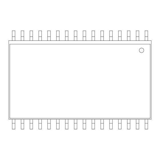
Page 8: Package Diagrams
Package Diagrams 32 LD (450 Mil) SOIC 0.793[20.142] 0.817[20.751] 0.101[2.565] 0.111[2.819] 0.050[1.270] BSC. 0.014[0.355] 0.020[0.508] 32-Lead Thin Small Outline Package Type II (51-85095) Document #: 001-06517 Rev. *A 32-lead (450-Mil) Molded SOIC (51-85081) 0.546[13.868] 0.566[14.376] 0.440[11.176] DIMENSIONS IN INCHES[MM] 0.450[11.430] PACKAGE WEIGHT 1.42gms 0.006[0.152] 0.012[0.304]... - Page 9 Package Diagrams (continued) 32-lead Reverse Thin Small Outline Package Type II (51-85138) More Battery Life is a trademark, and MoBL is a registered trademark, of Cypress Semiconductor. All products and company names mentioned in this document may be the trademarks of their respective holders. Document #: 001-06517 Rev.
- Page 10 Document History Page ® Document Title: CY62148BN MoBL Document Number: 001-06517 Issue REV. ECN NO. Date 426504 See ECN 485639 See ECN Document #: 001-06517 Rev. *A 4-Mbit (512K x 8) Static RAM Orig. of Change Description of Change New Data Sheet Corrected the typo in the Array size in the Logic Block Diagram ®...
Need help?
Do you have a question about the MoBL CY62148BN and is the answer not in the manual?
Questions and answers