Table of Contents
Advertisement
Quick Links
EZ-OTG Features
• Single-chip programmable USB dual-role (Host/Peripheral)
controller with two configurable Serial Interface Engines
(SIEs) and two USB ports
• Supports USB OTG protocol
• On-chip 48-MHz 16-bit processor with dynamically
switchable clock speed
• Configurable IO block supports a variety of IO options or up
to 25 bits of General Purpose IO (GPIO)
• 4K × 16 internal mask ROM contains built-in BIOS that
supports a communication-ready state with access to I
EEPROM interface, external ROM, UART, or USB
• 8K x 16 internal RAM for code and data buffering
• 16-bit parallel host port interface (HPI) with DMA/Mailbox
data path for an external processor to directly access all
on-chip memory and control on-chip SIEs
• Fast serial port supports from 9600 baud to 2.0M baud
Block Diagram
CY7C67200
nRESET
Vbus, ID
D+,D-
HOST/
Peripheral
USB Ports
D+,D-
X1
X2
Cypress Semiconductor Corporation
Document #: 38-08014 Rev. *G
2
C™
CY7C67200
Timer 0
Control
Watchdog
16-bit RISC CORE
OTG
USB-A
SIE1
USB-A
4Kx16
ROM BIOS
SIE2
Mobile
PLL
Power
Booster
•
198 Champion Court
EZ-OTG™ Programmable USB
• SPI supports both master and slave
• Supports 12 MHz external crystal or clock
• 2.7V to 3.6V power supply voltage
• Package option: 48-pin FBGA
Typical Applications
EZ-OTG is a very powerful and flexible dual-role USB
controller that supports a wide variety of applications. It is
primarily intended to enable USB OTG capability in applica-
tions such as:
• Cellular phones
• PDAs and pocket PCs
• Video and digital still cameras
• MP3 players
• Mass storage devices
Timer 1
UART I/F
CY16
I2C
EEPROM I/F
HSS I/F
SPI I/F
8Kx16
RAM
HPI I/F
GPIO
,
•
San Jose
CA 95134-1709
CY7C67200
On-The-Go
GPIO [24:0]
•
408-943-2600
Revised November 14, 2006
[+] Feedback
Advertisement
Table of Contents

Related Manuals for Cypress EZ-OTG CY7C67200


Summary of Contents for Cypress EZ-OTG CY7C67200
- Page 1 EZ-OTG Features • Single-chip programmable USB dual-role (Host/Peripheral) controller with two configurable Serial Interface Engines (SIEs) and two USB ports • Supports USB OTG protocol • On-chip 48-MHz 16-bit processor with dynamically switchable clock speed • Configurable IO block supports a variety of IO options or up to 25 bits of General Purpose IO (GPIO) •...
-
Page 2: Interface Descriptions
Introduction EZ-OTG™ (CY7C67200) is Cypress Semiconductor’s first USB On-The-Go (OTG) host/peripheral controller. EZ-OTG is designed to easily interface to most high-performance CPUs to add USB host functionality. EZ-OTG has its own 16-bit RISC processor to act as a coprocessor or operate in standalone mode. - Page 3 USB Interface EZ-OTG has two built-in Host/Peripheral SIEs that each have a single USB transceiver, meeting the USB 2.0 specification requirements for full and low speed (high speed is not support- ed). In Host mode, EZ-OTG supports two downstream ports; each supports control, interrupt, bulk, and isochronous trans- fers.
- Page 4 UART Features • Supports baud rates of 900 to 115.2K • 8-N-1 UART Pins Table 5. UART Interface Pins Pin Name Pin Number C EEPROM Interface EZ-OTG provides a master-only I2C interface for external se- rial EEPROMs. The serial EEPROM can be used to store ap- plication-specific code and data.
- Page 5 Host Port Interface (HPI) EZ-OTG has an HPI interface. The HPI interface provides DMA access to the EZ-OTG internal memory by an external host, plus a bidirectional mailbox register for supporting high-level communication protocols. This port is designed to be the primary high-speed connection to a host processor. Complete control of EZ-OTG can be accomplished through this interface via an extensible API and communication protocol.
- Page 6 Charge Pump Features • Meets OTG Supplement Requirements, see Characteristics: Charge Pump,” on page Charge Pump Pins Table 11.Charge Pump Interface Pins Pin Name Pin Number OTGVBUS CSwitchA CSwitchB Booster Interface EZ-OTG has an on-chip power booster circuit for use with power supplies that range between 2.7V and 3.6V.
- Page 7 Crystal Pins Table 13.Crystal Pins Pin Name Pin Number XTALIN XTALOUT Boot Configuration Interface EZ-OTG can boot into any one of four modes. The mode it boots into is determined by the TTL voltage level of GPIO[31:30] at the time nRESET is deasserted. shows the different boot pin combinations possible.
- Page 8 Minimum Hardware Requirements for Standalone Mode – Peripheral Only Figure 5. Minimum Standalone Hardware Configuration – Peripheral Only VBus Standard-B or Mini-B SHIELD Up to 64k x8 EEPROM *Bootloading begins after POR + 3ms BIOS bootup *GPIO[31:30] Up to 2k x8 SCL SDA >2k x8 to 64k x8 SDA SCL...
-
Page 9: Memory Map
External (Remote) Wakeup Source There are several possible events available to wake EZ-OTG from Sleep mode as shown in Table 15. These may also be used as remote wakeup options for USB applications. section “Power Control Register [0xC00A] [R/W]” on page Upon wakeup, code begins executing within 200 ms, the time it takes the PLL to stabilize. - Page 10 Registers Some registers have different functions for a read vs. a write access or USB host vs. USB device mode. Therefore, registers of this type have multiple definitions for the same address. The default register values listed in this data sheet may be altered to some other value during BIOS initialization.
- Page 11 Bank Register [0xC002] [R/W] Bit # Field Read/Write Default Bit # Field ...Address Read/Write Default Register Description The Bank register maps registers R0–R15 into RAM. The eleven MSBs of this register are used as a base address for registers R0–R15. A register address is automatically generated by: 1.
- Page 12 CPU Speed Register [0xC008] [R/W] Bit # Field Read/Write Default Bit # Field ...Reserved Read/Write Default Register Description The CPU Speed register allows the processor to operate at a user selected speed. This register only affects the CPU; all other peripheral timing is still based on the 48-MHz system clock (unless otherwise noted).
- Page 13 Power Control Register [0xC00A] [R/W] Bit # Reserved Host/Device 2 Field Wake Enable Read/Write Default Bit # Reserved Field Wake Enable Read/Write Default Register Description The Power Control register controls the power-down and wakeup options. Either the sleep mode or the halt mode options can be selected.
- Page 14 Halt Enable (Bit 0) Setting this bit to ‘1’ immediately initiates HALT mode. While in HALT mode, only the CPU is stopped. The internal clock still runs and all peripherals still operate, including the USB engines. The power savings using HALT in most cases will be minimal, but in applications that are very CPU intensive the incremental savings may provide some benefit.
- Page 15 UART Interrupt Enable (Bit 3) The UART Interrupt Enable bit enables or disables the following UART hardware interrupts: UART TX and UART RX. 1: Enable UART interrupt 0: Disable UART interrupt GPIO Interrupt Enable (Bit 2) The GPIO Interrupt Enable bit enables or disables the General Purpose IO Pins Interrupt (See the GPIO Control Register).
- Page 16 USB Diagnostic Register [0xC03C] [R/W] Bit # Reserved Port 2A Diagnostic Field Enable Read/Write Default Bit # ...Reserved Pull-down Field Enable Read/Write Default Register Description The USB Diagnostic Register provides control of diagnostic modes. It is intended for use by device characterization tests, not for normal operations.
- Page 17 Watchdog Timer Register [0xC00C] [R/W] Bit # Field Read/Write Default Bit # ...Reserved Field Read/Write Default Register Description The Watchdog Timer register provides status and control over the Watchdog timer. The Watchdog timer can also interrupt the processor. Timeout Flag (Bit 5) The Timeout Flag bit indicates if the Watchdog timer has expired.
- Page 18 Timer n Register [R/W] • Timer 0 Register 0xC010 • Timer 1 Register 0xC012 Bit # Field Read/Write Default Bit # Field Read/Write Default Register Description The Timer n Register sets the Timer n count. Both Timer 0 and Timer 1 decrement by one every 1-µs clock tick. Each can provide an interrupt to the CPU when the timer reaches zero.
- Page 19 Port A D+ Status (Bit 13) The Port A D+ Status bit is a read-only bit that indicates the value of DATA+ on Port A. 1: D+ is high 0: D+ is low Port A D– Status (Bit 12) The Port A D– Status bit is a read-only bit that indicates the value of DATA–...
- Page 20 Host n Control Register [R/W] • Host 1 Control Register 0xC080 • Host 2 Control Register 0xC0A0 Bit # Field Read/Write Default Bit # Preamble Sequence Field Enable Select Read/Write Default Register Description The Host n Control register allows high-level USB transaction control.
- Page 21 Host n Address Register [R/W] • Host 1 Address Register 0xC082 • Host 2 Address Register 0xC0A2 Bit # Field Read/Write Default Bit # Field Read/Write Default Register Description The Host n Address register is used as the base pointer into memory space for the current host transactions.
- Page 22 Host n Endpoint Status Register [R] • Host 1 Endpoint Status Register 0xC086 • Host 2 Endpoint Status Register 0xC0A6 Bit # Reserved Field Read/Write Default Bit # Stall Flag Flag Field Read/Write Default Register Description The Host n Endpoint Status register is a read-only register that provides status for the last USB transaction.
- Page 23 ACK Flag (Bit 0) The ACK Flag bit indicates two different conditions depending on the transfer type. For non-Isochronous transfers, this bit represents a transaction ending by receiving or sending an ACK packet. For Isochronous transfers, this bit represents a successful transaction that will not be represented by an ACK packet.
- Page 24 Host n Count Result Register [R] • Host 1 Count Result Register 0xC088 • Host 2 Count Result Register 0xC0A8 Bit # Field Read/Write Default Bit # Field Read/Write Default Register Description The Host n Count Result register is a read-only register that contains the size difference in bytes between the Host Count Value specified in the Host n Count register and the last packet received.
- Page 25 Host n Interrupt Enable Register [R/W] • Host 1 Interrupt Enable Register 0xC08C • Host 2 Interrupt Enable Register 0xC0AC Bit # VBUS ID Interrupt Field Interrupt Enable Enable Read/Write Default Bit # Reserved Port A Wake Interrupt Enable Field Read/Write Default Register Description...
- Page 26 Host n Status Register [R/W] • Host 1 Status Register 0xC090 • Host 2 Status Register 0xC0B0 Bit # VBUS ID Interrupt Field Interrupt Flag Flag Read/Write Default Bit # Reserved Port A Wake Interrupt Field Flag Read/Write Default Register Description The Host n Status register provides status information for host operation.
- Page 27 Host n SOF/EOP Count Register [R/W] • Host 1 SOF/EOP Count Register 0xC092 • Host 2 SOF/EOP Count Register 0xC0B2 Bit # Field Reserved Read/Write Default Bit # Field Read/Write Default Register Description The Host n SOF/EOP Count register contains the SOF/EOP Count Value that is loaded into the SOF/EOP counter.
- Page 28 Host n Frame Register [R] • Host 1 Frame Register 0xC096 • Host 2 Frame Register 0xC0B6 Bit # Field Read/Write Default Bit # Field Read/Write Default Register Description The Host n Frame register maintains the next frame number to be transmitted (current frame number + 1). This value is updated after each SOF transmission.
- Page 29 Figure 30. Device n Endpoint n Control Register Bit # Field Read/Write Default Bit # IN/OUT Sequence Ignore Select Field Enable Read/Write Default Register Description The Device n Endpoint n Control register provides control over a single EP in device mode. There are a total of eight endpoints for each of the two ports.
- Page 30 Device n Endpoint n Address Register [R/W] • Device n Endpoint 0 Address Register [Device 1: 0x0202 Device 2: 0x0282] • Device n Endpoint 1 Address Register [Device 1: 0x0212 Device 2: 0x0292] • Device n Endpoint 2 Address Register [Device 1: 0x0222 Device 2: 0x02A2] •...
- Page 31 Register Description The Device n Endpoint n Count register designates the maximum packet size that can be received from the host for OUT transfers for a single endpoint. This register also designates the packet size to be sent to the host in response to the next IN token for a single endpoint.
- Page 32 IN Exception Flag (Bit 8) The IN Exception Flag bit indicates when the device received an IN packet when armed for an OUT. 1: Received IN when armed for OUT 0: Received OUT when armed for OUT Stall Flag (Bit 7) The Stall Flag bit indicates that a Stall packet was sent to the host.
- Page 33 Device n Endpoint n Count Result Register [R/W] • Device n Endpoint 0 Count Result Register [Device 1: 0x0208 Device 2: 0x0288] • Device n Endpoint 1 Count Result Register [Device 1: 0x0218 Device 2: 0x0298] • Device n Endpoint 2 Count Result Register [Device 1: 0x0228 Device 2: 0x02A8] •...
- Page 34 Device n Interrupt Enable Register [R/W] • Device 1 Interrupt Enable Register 0xC08C • Device 2 Interrupt Enable Register 0xC0AC Figure 35. Device n Interrupt Enable Register Bit # VBUS ID Interrupt Interrupt Enable Field Enable Read/Write Default Bit # EP7 Interrupt EP6 Interrupt Field...
- Page 35 EP5 Interrupt Enable (Bit 5) The EP5 Interrupt Enable bit enables or disables an endpoint five (EP5) Transaction Done interrupt. An EPx Transaction Done interrupt triggers when any of the following responses or events occur in a transaction for the device’s given Endpoint: send/receive ACK, send STALL, Timeout occurs, IN Exception Error, or OUT Exception Error.
- Page 36 Device n Address Register [W] • Device 1 Address Register 0xC08E • Device 2 Address Register 0xC0AE Bit # Field Read/Write Default Bit # Field ...Reserved Read/Write Default Register Description The Device n Address register holds the device address assigned by the host. This register initializes to the default address 0 at reset but must be updated by firmware when the host assigns a new address.
- Page 37 Reset Interrupt Flag (Bit 8) The Reset Interrupt Flag bit indicates if the USB Reset Detected interrupt has triggered. 1: Interrupt triggered 0: Interrupt did not trigger EP7 Interrupt Flag (Bit 7) The EP7 Interrupt Flag bit indicates if the endpoint seven (EP7) Transaction Done interrupt has triggered.
- Page 38 Device n Frame Number Register [R] • Device 1 Frame Number Register 0xC092 • Device 2 Frame Number Register 0xC0B2 Bit # SOF/EOP Field Timeout Flag Timeout Interrupt Counter Read/Write Default Bit # Field Read/Write Default Register Description The Device n Frame Number register is a read only register that contains the Frame number of the last SOF packet received.
- Page 39 OTG Control Registers There is one register dedicated for OTG operation. This register is covered in this section and summarized in OTG Control Register [0xC098] [R/W] Bit # Field Reserved Read/Write Default Bit # Field D– Pull-down Pull-down Enable Enable Read/Write Default Register Description...
- Page 40 VBUS Valid Flag (Bit 0) The VBUS Valid Flag bit indicates whether OTG VBus is greater than 4.4V. After turning on VBUS, firmware should wait at least 10 µs before this reading this bit. GPIO Registers There are seven registers dedicated for GPIO operations. These seven registers are covered in this section and summarized in Table Table 29.GPIO Registers Register Name...
- Page 41 HSS Enable (Bit 7) The HSS Enable bit routes HSS to GPIO[15:12]. 1: HSS is routed to GPIO 0: HSS is not routed to GPIOs. GPIO[15:12] are free for other purposes. SPI Enable (Bit 5) The SPI Enable bit routes SPI to GPIO[11:8]. If the SAS Enable bit is set, it overrides and routes the SPI_nSSI pin to GPIO15.
- Page 42 Writing a 1 to any bit will output a high voltage on the corresponding GPIO pin. Reserved All reserved bits must be written as ‘0’. GPIO 0 Input Data Register [0xC020] [R] Bit # Field GPIO15 GPIO14 Read/Write Default Bit # Field GPIO7 GPIO6...
- Page 43 Register Description The GPIO 0 Direction register controls the direction of the GPIO data pins (input/output). The GPIO 0 Direction register controls GPIO15 to GPIO0 while the GPIO 1 Direction register controls GPIO31 to GPIO19. When any bit of this register is set to ‘1’, the corresponding GPIO data pin becomes an output. When any bit of this register is set to ‘0’, the corresponding GPIO data pin becomes an input.
- Page 44 HSS Control Register [0xC070] [R/W] Bit # Enable Polarity Select Field Read/Write Default Bit # Transmit Receive Done Interrupt Done Interrupt Field Enable Enable Read/Write Default Register Description The HSS Control register provides high-level status and control over the HSS port. HSS Enable (Bit 15) The HSS Enable bit enables or disables HSS operation.
- Page 45 Transmit Ready (Bit 4) The Transmit Ready bit is a read only bit that indicates if the HSS Transmit FIFO is ready for the CPU to load new data for transmission. 1: HSS transmit FIFO ready for loading 0: HSS transmit FIFO not ready for loading Packet Mode Select (Bit 3) The Packet Mode Select bit selects between Receive Packet Ready and Receive Ready as the interrupt source for the...
- Page 46 HSS Transmit Gap Register [0xC074] [R/W] Bit # Field Read/Write Default Bit # Field Read/Write Default Register Description The HSS Transmit Gap register is only valid in block transmit mode. It allows for a programmable number of stop bits to be inserted thus overwriting the One Stop Bit in the HSS Control register.
- Page 47 HSS Receive Address Register [0xC078] [R/W] Bit # Field Read/Write Default Bit # Field Read/Write Default Register Description The HSS Receive Address register is used as the base pointer address for the next HSS block receive transfer. Address (Bits [15:0]) The Address field sets the base pointer address for the next HSS block receive transfer.
- Page 48 HSS Transmit Address Register [0xC07C] [R/W] Bit # Field Read/Write Default Bit # Field Read/Write Default Register Description The HSS Transmit Address register is used as the base pointer address for the next HSS block transmit transfer. Address (Bits [15:0]) The Address field sets the base pointer address for the next HSS block transmit transfer.
- Page 49 HPI Breakpoint Register [0x0140] [R] Bit # Field Read/Write Default Bit # Field Read/Write Default Register Description The HPI Breakpoint register is a special on-chip memory location, which the external processor can access using normal HPI memory read/write cycles. This register is read-only by the CPU but is read/write by the HPI port. The contents of this register have the same effect as the Breakpoint register [0xC014].
- Page 50 SOF/EOP2 to CPU Enable (Bit 12) The SOF/EOP2 to CPU Enable bit routes the SOF/EOP2 interrupt to the on-chip CPU. Since the SOF/EOP2 interrupt can be routed to both the on-chip CPU and the HPI port the firmware must ensure only one of the two (CPU, HPI) resets the interrupt.
- Page 51 SIEXmsg Register [W] • SIE1msg Register 0x0144 • SIE2msg Register 0x0148 Bit # Field Read/Write Default Bit # Field Read/Write Default Register Description The SIEXmsg register allows an interrupt to be generated on the HPI port. Any write to this register causes the SIEXmsg flag in the HPI Status Port to go high and also causes an interrupt on the HPI_INTR pin.
- Page 52 HPI Status Port [] [HPI: R] Bit # VBUS Field Flag Flag Read/Write Default Bit # Resume2 Resume1 Field Flag Flag Read/Write Default Register Description The HPI Status Port provides the external host processor with the MailBox status bits plus several SIE status bits. This register is not accessible from the on-chip CPU.
- Page 53 mode this read only bit indicates if any of the endpoint inter- rupts occurs on Device 2. Firmware needs to determine which endpoint interrupt occurred. 1: Interrupt triggered 0: Interrupt did not trigger Done1 Flag (Bit 2) In host mode the Done 1 Flag bit is a read-only bit that indicates if a host packet done interrupt occurs on Host 1.
- Page 54 3Wire Enable (Bit 15) The 3Wire Enable bit indicates if the MISO and MOSI data lines are tied together allowing only half duplex operation. 1: MISO and MOSI data lines are tied together 0: Normal MISO and MOSI Full Duplex operation (not tied together) Phase Select (Bit 14) The Phase Select bit selects advanced or delayed SCK phase.
- Page 55 SPI Control Register [0xC0CA] [R/W] Bit # FIFO Field Strobe Init Read/Write Default Bit # Transmit Receive Field Empty Full Read/Write Default Register Description The SPI Control register controls the SPI port. Fields apply to both master and slave mode unless otherwise noted. SCK Strobe (Bit 15) The SCK Strobe bit starts the SCK strobe at the selected frequency and polarity (set in the SPI Configuration register),...
- Page 56 Receive Bit Length (Bits [2:0]) The Receive Bit Length field controls whether a full byte or partial byte will be received. If Receive Bit Length is ‘000’ then a full byte will be received. If Receive Bit Length is ‘001’ to ‘111’, then the value indicates the number of bits that will be received. SPI Interrupt Enable Register [0xC0CC] [R/W] Bit # Field...
- Page 57 Transmit Interrupt Flag (Bit 1) The Transmit Interrupt Flag is a read only bit that indicates a byte mode transmit interrupt has triggered. 1: Indicates a byte mode transmit interrupt has triggered 0: Indicates a byte mode transmit interrupt has not triggered SPI Interrupt Clear Register [0xC0D0] [W] Bit # Field...
- Page 58 CRC Enable (Bit 13) The CRC Enable bit enables or disables the CRC operation. 1: Enables CRC operation 0: Disables CRC operation CRC Clear (Bit 12) The CRC Clear bit will clear the CRC with a load of all ones. This bit is self clearing and always reads ‘0’.
- Page 59 Data Ready bit of the SPI Control register is set to ‘1’. Writing to this register in PIO byte mode will initiate a transfer of data, the number of bits defined by Transmit Bit Length field in the SPI Control register. Data (Bits [7:0]) The Data field contains data received or to be transmitted on the SPI port.
- Page 60 SPI Receive Address Register [0xC0DC [R/W] Bit # Field Read/Write Default Bit # Field Read/Write Default Register Description The SPI Receive Address register is issued as the base address for the SPI Receive DMA. Address (Bits [15:0]) The Address field sets the base address for the SPI receive DMA. SPI Receive Count Register [0xC0DE] [R/W] Bit # Field...
- Page 61 UART Control Register [0xC0E0] [R/W] Bit # Field Read/Write Default Bit # ...Reserved Field Read/Write Default Register Description The UART Control register enables or disables the UART allowing GPIO7 (UART_TXD) and GPIO6 (UART_RXD) to be freed up for general use. This register must also be written to set the baud rate, which is based on a 48-MHz clock.
- Page 62 Receive Full (Bit 1) The Receive Full bit indicates whether the receive buffer is full. It can be programmed to interrupt the CPU as interrupt #5 when the buffer is full. This can be done though the UART bit of the Interrupt Enable register (0xC00E). This bit will automat- ically be cleared when data is read from the UART Data register.
-
Page 63: Pin Descriptions
Pin Diagram The following describes the CY7C67200 48-pin FBGA. Figure 76. EZ-OTG Pin Diagram GPIO3/D3 GPIO1/D1 AGND GPIO0/D0 GPIO4/D4 GPIO2/D2 OTGVBUS DM2A CSWITCHA CSWITCHB DP2A BOOSTGND VSWITCH DP1A BOOSTVCC DM1A GPIO30/SDA AVCC XTALOUT XTALIN GPIO31/SCL Pin Descriptions Table 38.Pin Descriptions Name GPIO31/SCK GPIO30/SDA... - Page 64 Table 38.Pin Descriptions (continued) Name GPIO20/A1 GPIO19/A0 GPIO15/D15/CTS/ nSSI GPIO14/D14/RTS GPIO13/D13/RXD GPIO12/D12/TXD GPIO11/D11/MOSI GPIO10/D10/SCK GPIO9/D9/nSSI GPIO8/D8/MISO GPIO7/D7/TX GPIO6/D6/RX GPIO5/D5 GPIO4/D4 GPIO3/D3 GPIO2/D2 GPIO1/D1 GPIO0/D0 DM1A DP1A DM2A DP2A XTALIN XTALOUT nRESET Document #: 38-08014 Rev. *G Type Description GPIO20: General Purpose IO A1: HPI A1 GPIO19: General Purpose IO A0: HPI A0...
-
Page 65: Absolute Maximum Ratings
Table 38.Pin Descriptions (continued) Name Reserved BOOSTV VSWITCH BOOSTGND OTGVBUS CSWITCHA CSWITCHB AGND H2, D6, A4 G6, B6, A1, H1 Absolute Maximum Ratings This section lists the absolute maximum ratings. Stresses above those listed can cause permanent damage to the device. Exposure to maximum rated conditions for extended periods can affect device operation and reliability. - Page 66 DC Characteristics Table 40.DC Characteristics Parameter Description , AV Supply Voltage BoosV Supply Voltage Input HIGH Voltage Input LOW Voltage Input Leakage Current Output Voltage HIGH Output LOW Voltage Output Current HIGH Output Current LOW Input Pin Capacitance Hysteresis on nReset Pin [7, 8] Supply Current [7, 8]...
-
Page 67: Reset Timing
Table 41.DC Characteristics: Charge Pump (continued) Parameter Description A-Device Session Valid A_SESS_VALID B-Device Session Valid B_SESS_VALID B-Device Session End A_SESS_END Efficiency When Loaded Data Line Pull Down A-device V Input Impedance A_BUS_IN to GND B-device V SRP Pull Up B_SRP_UP B-device V SRP Pull Down B_SRP_DWN... -
Page 68: Clock Timing
Clock Timing XTALIN HIGH Parameter Description Clock Frequency [10] Clock Input High XINH (XTALOUT left floating) Clock Period Clock High Time HIGH Clock Low Time Clock Rise Time RISE Clock Fall Time FALL Duty Cycle C EEPROM Timing 1. I2C EEPROM Bus Timing - Serial I/O SU.STA HD.STA SDA IN... - Page 69 HPI (Host Port Interface) Write Cycle Timing ADDR [1:0] CSSU Dout [15:0] Parameter Description Address Setup Address Hold Chip Select Setup CSSU Chip Select Hold Data Setup Write Data Hold Write Pulse Width Write Cycle Time Note 11. T = system clock period = 1/48 MHz. Document #: 38-08014 Rev.
- Page 70 HPI (Host Port Interface) Read Cycle Timing ADDR [1:0] CSSU Din [15:0] Parameter Description Address Setup Address Hold Chip Select Setup CSSU Chip Select Hold Data Access Time, from HPI_nRD falling Read Data Hold, relative to the earlier of HPI_nRD rising or HPI_nCS rising Read Pulse Width Read Cycle Time...
- Page 71 HSS BYTE Mode Transmit qt_clk CPU_A[2:0] CPUHSS_cs CPU_wr TxRdy flag HSS_TxD Byte transmit triggered by a CPU write to the HSS_TxData register qt_clk, CPU_A, CPUHSS_cs, CPU_wr are internal signals, included in the diagram to illustrate relationship between CPU opera- tions and HSS port operations. Bit 0 is LSB of data byte.
- Page 72 Hardware CTS/RTS Handshake tCTShold tCTSsetup HSS_RTS HSS_CTS HSS_TxD Start of transmission delayed until HSS_CTS goes high : HSS_CTS setup time before HSS_RTS = 1.5T min. CTSset-up : HSS_CTS hold time after START bit = 0 ns min. CTShold T = 1/48 MHz. When RTS/CTS hardware handshake is enabled, transmission can be held off by deasserting HSS_CTS at least 1.5T before HSS_RTS.
-
Page 73: Register Summary
Register Summary Table 42. Register Summary Address Register Bit 15 Bit 7 0x0140 HPI Breakpoint Address..Address 0x0142 Interrupt Routing VBUS to HPI Enable Resume2 to HPI Enable 1: 0x0144 SIEXmsg Data... 2: 0x0148 ...Data 0x02n0 Device n Endpoint n Control Reserved IN/OUT Ignore Enable... - Page 74 Table 42. Register Summary (continued) Address Register Bit 15 Bit 7 0xC024 GPIO 1 Output Data GPIO31 GPIO23 0xC026 GPIO 1 Input Data GPIO31 GPIO23 0xC028 GPIO 1 Direction GPIO31 GPIO23 0xC03C USB Diagnostic Reserved ...Reserved 0xC070 HSS Control Enable Transmit Done Interrupt Flag 0xC072...
- Page 75 Table 42. Register Summary (continued) Address Register Bit 15 Bit 7 0xC090 Host 1 Status VBUS Interrupt Flag Reserved 0xC090 Device 1 Status VBUS Interrupt Flag Interrupt Flag 0xC092 Host n SOF/EOP Count Reserved 0xC0B2 ...Count 0xC092 Device n Frame Number SOF/EOP 0xC0B2 Timeout...
- Page 76 Table 42. Register Summary (continued) Address Register Bit 15 Bit 7 0xC0D6 SPI Data Port t Reserved Data 0xC0D8 SPI Transmit Address Address..Address 0xC0DA SPI Transmit Count Reserved ...Count 0xC0DC SPI Receive Address Address..Address 0xC0DE SPI Receive Count Reserved ...Count 0xC0E0...
-
Page 77: Ordering Information
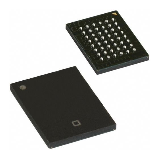
Ordering Information Table 43.Ordering Information Ordering Code CY7C67200-48BAXI 48FBGA CY7C67200-BAXIT 48FBGA, Tape and reel CY3663 Development Kit Package Diagram 48-Ball (7.00 mm x 7.00 mm x 1.2 mm) FBGA BA48 TOP VIEW PIN 1 CORNER (LASER MARK) 7.00±0.10 SEATING PLANE Purchase of I C™... - Page 78 Document History Page Document Title: CY7C67200 EZ-OTG™ Programmable USB On-The-Go Host/Peripheral Controller Document Number: 38-08014 Issue REV. ECN NO. Date 111872 03/22/02 116988 08/23/02 124954 04/10/03 126211 05/23/03 127334 05/29/03 129394 10/07/03 472875 See ECN 567317 See ECN KKVTMP Added the lead free information on the Ordering Information Section. Imple- Document #: 38-08014 Rev.
Need help?
Do you have a question about the EZ-OTG CY7C67200 and is the answer not in the manual?
Questions and answers